Currently, in the era of big data and 5G communication technology, electromigration has become a serious reliability issue for the miniaturized solder joints used in microelectronic devices. Since the effective charge number (Z*) is considered as the driving force for electromigration, the lack of accurate experimental values for Z* poses severe challenges for the simulation-aided design of electronic materials. In this work, a data-driven framework is developed to predict the Z* values of Cu and Sn species at the anode based LIQUID, Cu6Sn5 intermetallic compound (IMC) and FCC phases for the binary Cu-Sn system undergoing electromigration at 523.15 K. The growth rate constants (kem) of the anode IMC at several magnitudes of applied low current density (j = 1 × 10⁶ to 10 × 106 A/m2) are extracted from simulations based on a 1D multi-phase field model. A neural network employing Z* and j as input features, whereas utilizing these computed kem data as the expected output is trained. The results of the neural network analysis are optimized with experimental growth rate constants to estimate the effective charge numbers. For a negligible increase in temperature at low j values, effective charge numbers of all phases are found to increase with current density and the increase is much more pronounced for the IMC phase. The predicted values of effective charge numbers Z* are then utilized in a 2D simulation to observe the anode IMC grain growth and electrical resistance changes in the multi-phase system. As the work consists of the aspects of experiments, theory, computation, and machine learning, it can be called the four paradigms approach for the study of electromigration in Pb-free solder. Such a combination of multiple paradigms of materials design can be problem-solving for any future research scenario that is marked by uncertainties regarding the determination of material properties.
Keywords:Phase field method
;
Artificial neural network
;
Intermetallic compound
;
Current density
;
Synchrotron radiation
Anil Kunwar, Yuri Amorim Coutinho, Johan Hektor, Haitao Ma, Nele Moelans. Integration of machine learning with phase field method to model the electromigration induced Cu6Sn5 IMC growth at anode side Cu/Sn interface. Journal of Materials Science & Technology[J], 2020, 59(0): 203-219 DOI:10.1016/j.jmst.2020.04.046
1. Introduction
In this era of big data and miniaturized microelectronic devices, the growing trend for the use of 5G communication technology in artificial intelligence (AI) applications, has provided the microelectronics industries an impetus to promote 2.5D integrated circuits (2.5D IC) devices into mass production [1]. Compared to 2D IC devices, 2.5D IC devices require one more redistribution layer (RDL) and, subsequently, one more level of solder joints owing to the use of vertical interconnects. This makes the solder joints of the 2.5D devices more vulnerable to electromigration induced failures. Electromigration is defined as the process in which materials or species transport occurs due to a gradient in electric potential [2]. With the advancements in the joining technology, the continuous downscaling of solder joints has become a major paradigm in electronic packaging industries (in accordance with Moore’s law), and this miniaturization of the joints has caused electromigration to be a major reliability concern [[3], [4], [5], [6], [7], [8]]. In the context of sub-100 nm structures, the current density during device operation may reach several mA/cm2 [3]. The localized temperature raise caused by Joule heating can then become high enough to melt some parts of the Sn-based solder joint. For example, localized spots with anode temperatures above 250 °C [9] have been experimentally observed for a Cu/30 μm-Sn/Cu joint stressed with a current density of 1.3 × 10⁴-1.5 × 10⁴ A/cm2. In this sense, characterization and prediction of the electromigration behavior in liquid solder have become a necessity in reliability studies.
The driving force for electromigration ${{\bar{F}}_{\text{em}}}$ is expressed using a dimensionless parameter, the effective charge number (Z*) [10], as follows:
${{\bar{F}}_{\text{em}}}=e{{Z}^{*}}\rho j$
where e is the charge of an electron, E is the electric field intensity, ρ is the electric resistivity of the phase, and j is the current density. Actually, the effective charge number is the sum of the electrostatic charge number (Ze) and the electron wind charge number (Zw) [11]. Accordingly, the electromigration driving force is comprised of an electrostatic and an electron wind contribution [10,[12], [13], [14], [15], [16]]:
where Ze represents the direct electrostatic force on the moving ion, and its value is equal to the nominal valence of the ion. The contribution Zw accounts for the electron wind force, which is generally the dominant contribution during practical electromigration in metallic joints and interfaces.
The electromigration parameters, such as electric resistivity and current density can be measured. However, there is no relevant work till now which ascertains accurate values of effective charge numbers (Z*) in binary, ternary, or in general, multicomponent alloys. This induces uncertainty in the quantification of the overall electromigration driving force for phase evolution. For a multiphase system consisting of more than one component undergoing electromigration, the major difficulty is in quantifying the electron wind charge number (Zw) [13,15,16].
For the binary Cu-Sn system consisting of Cu-rich, Sn-rich, and intermetallic phases, a multiphase field formalism [17] has been utilized to investigate the evolution of interfacial intermetallic compound (IMC) layers under electromigration conditions [[18], [19], [20]]. The research works [[18], [19], [20]] utilize a free energy density term to describe the electromigration driving force on phase evolution, and this term includes the effective charge number. As highlighted earlier, it is not clearly understood how the magnitude of Z* has been assigned in these works. In the work by Zhou and Johnson [18], the magnitudes of effective charge number for generalized species A and B are respectively taken as 90 and 0, but these values are constants in all the three phases considered. Park et al. [19] have assigned a constant magnitude of 50 for effective charge numbers, implying that both Cu and Sn are considered to have the same value Z* for all of the FCC, IMCs, and BCT phases. Though Attari et al. [20] took different values of the effective charge numbers in different phases, they assumed that the numbers for Cu and Sn are of the same magnitude in the same phase. Chao et al. [10] stated that for the binary Cu-Sn system, in general, the effective charge numbers of Cu and Sn are not equal and are also different in different phases.
It can be expected that the growth behavior of the intermetallic layer at the anode Cu/Sn interface is primarily affected by interdiffusion and electromigration [10]. Hence, if the diffusion parameters are well known, the effective charge number can be inferred back by comparing experimentally determined growth rates of the IMC layer with growth rates obtained from simulations combining interdiffusion and electromigration and assuming a range of electromigration parameter values. An important difficulty is then that, at higher current densities, the temperature of the Cu-Sn system increases considerably due to Joule heating, resulting in considerable fluctuations in the value of the interdiffusion coefficients, complicating an accurate determination of the electromigration parameters. However, at lower current density (< 10 × 106 A/m2), the temperature rise is found to be negligible [2], and constant values of the diffusivities in the different phases can therefore be assumed in the procedure to predict the electromigration parameters.
On the one hand, multi-phase field methods can integrate multi-physics data of electromigration and interdiffusion parameters to uncover mechanisms that explain the emergence of anode Cu6Sn5 IMC growth kinetics. On the other hand, machine learning can integrate multimodality and multifidelity data, thus helping to reveal correlations between intertwined phenomena, such as growth kinetics and the effective charge number of the different elements in the different phases. In this regard, machine learning and phase field method can naturally complement each other and will enable us to create strong predictive models that integrate the underlying physics and explore massive material design spaces including the effect of electromigration [21]. Moreover, multiphysical models (finite element analysis), when coupled with experimental observation, can be utilized to construct the dataset for the machine learning model. It has been demonstrated in [22] that finite element method generated (FEM-generated) data for given laser soldering experiments can be used to train the neural network, for prediction of the morphology of interfacial intermetallic compound (IMC).
In the sector of materials design and discovery, data-driven materials science has emerged as the fourth scientific paradigm following the first three paradigms-experiments, theory and computation [23]. In our present work and as presented in Fig. 1, we employ these four paradigms - (I) Experiments, (II) Theory, (III) Computation and (IV) Machine learning in a combined way, to understand the materials science of anode interface in Cu-Sn binary system undergoing electromigration. With the relevant phases outlined through in-situ experimental imaging, phase field (PF) simulation will be performed in this work to integrate the data of electromigration parameters -j and, phase and composition dependent Z* with the spatio-temporal evolution of anode IMC phase. The work will focus on cases with low current density to avoid the complexities associated with Joule heating at high current density. For the phase field simulations generated datasets, neural network analysis will be done to predict the growth rate constant at given input values of j and Z*. The growth rate constant is then optimized with available experimental data obtained from the thickness measurement of the cross-sectional image of the anode interface. Using the inverse design, the neural network is then used to estimate the optimum effective charge numbers for Cu and Sn in different phases. These Z* values will be used in a 2D phase field model to study IMC grain growth due to interdiffusion and electromigration. For better performance of electronic devices and solar photovoltaic modules, the interconnections and joints utilized in these devices and systems must be characterized with good electrical and thermal conductances [24,25]. Since the intermetallic grains have different electrical resistivity compared to pure Sn and pure Cu metals, the accelerated growth of IMC phases due to electromigration causes the change in the electrical resistance of the overall system, and a method to compute the change in electrical resistance due to the microstructural evolution of phases is also included in the present work.
Fig. 1.
Experimental tools (paradigm I) are utilized to ascertain the phases at the material interface, and also to perform the validation work during inverse design of electromigration parameters. The theoretical equations (paradigm II) are solved computationally in the finite element method based computational model (paradigm III). The artificial neural network (ANN, paradigm IV) is used to predict the effective charge number. And finally, with all the quantities determined, the FEM is used to compute the electrical resistance in the multiphase system.
2. Experimental methods for data preparation
In the context of experimental electromigration tests, the interfaces that have been characterized ex-situ can be utilized as a source growth kinetics data, but for the validation of the interfacial phases required by the multiphase field model, in-situ experiments are the proper choices. The in-situ synchrotron radiation (SR) X-ray imaging technology offers a promising strategy to observe in real-time and precisely distinguish exact phases formed and evolved as a result of diffusion and electromigration in experimental sample. In-situ synchrotron radiation radiography experiments (Fig. 2) for the electromigration test of present work were performed in the beamline BL13W1 of Shanghai Synchrotron Radiation Facility (SSRF), Shanghai, China. As shown in Fig. 2(i), liquid Sn is sandwiched between two Cu substrates at the ambient temperature maintained at 523.15 K. The two Cu substrates are then connected by electrical wires to the DC voltage source. The Cu electrode connected to the negative terminal of the battery is anode whereas another Cu substrate linked to the positive terminal is the cathode (illustrated in Fig. 3(a). The Sn-rich liquid media of length 450 μm across interfaces, has larger electric resistivity than the electrodes and is the conducting media for current flowing from anode to the cathode terminal. The thickness of liquid Sn (maintained by ceramic supports) and Cu electrodes was designed as 100 μm so that the X-ray beam passing through these thin films can produce images of high contrast between the phases. The energy of the monochromatic X-ray beam was set as 28 keV. A charge coupled device (CCD) camera was kept at a distance of 200 mm from the sample, and the parameters of the CCD camera such as resolution ratio and exposure time were set as 0.74 μm/pix and 4 s, respectively. More details of the experimental parameters associated with the synchrotron radiation imaging technology for the electromigration test at a constant current density of 5.6 × 10⁶ A/m2 is described in [26]. The images shown in Fig. 2(ii) depict the asymmetrical growth of interfacial intermetallic compound (IMC) phases at the two FCC (Cu-rich phase)/LIQUID (Sn-rich phase) interfaces. In the context of image (a) corresponding to t =5 min, the IMC layers are not noticeable at either interface. At t = 10 min, the anode side interface’s IMC, yet difficult to measure, is visible whereas the IMC layer at the cathode interface is still not visible. However, in the image (d) at t = 45 min, it can be seen that the anode based IMC is asymmetrically larger, and still the cathode side IMC layer is not noticeable. The bubble present at the vicinity of anode interface being progressively engulfed with the IMC grains as time proceeds from 10 min to 25 min validates the electromigration influenced rapid growth of the IMC layer therein. At 45 min, the bubble is merged deep within the IMC layer.
Fig. 2.
Experimental setup at beamline BL13W1 of SSRF for obtaining in-situ synchrotron radiation (SR) radiography images of electromigration tests at T = 523.15 K, is schematically sketched in (i). Asymmetrical growth of anode based IMC phase at t = (a) 5, (b) 10, (c) 25, and (d) 45 min for Cu/Sn/Cu joint undergoing electromigration can be clearly noticed in (ii).
Fig. 3.
Schematic sketch to classify the anode and cathode electrodes in the Cu/Sn/Cu joint undergoing electromigration (a), outline the relevant phase at the anode interfaces for computational model (b).
It is interesting to note from Fig. 2(ii) that the phases observed in the electromigration experiment at t = 45 min are FCC (both at anode and cathode), Cu6Sn5 IMC at the anode interface, and LIQUID. Though the formation of Cu3Sn IMC between FCC phase and Cu6Sn5 IMC at anode interface is also thermodynamically favorable, the diffusion based growth kinetics of Cu3Sn IMC (interfaced between two solid state phases) is quite negligible compared to Cu6Sn5 IMC (remaining in contact with the LIQUID phase too). However, at lower temperatures, when both Cu substrate and Sn solder are in solid states, and the experiment is performed for a few days, the layer thickness of both Cu3Sn and Cu6Sn5 IMCs are comparable [27]. In this present study, when the solder is in LIQUID state and the experiment is performed for 1 h, the growth of only one IMC, namely, Cu6Sn5 IMC, is considered at the anode (Fig. 3(b)), and thus Cu3Sn IMC phase has been ignored. These experimentally observed three phases at anode interface - FCC, Cu6Sn5 IMC (mentioned as IMC hereafter) and LIQUID, are used for setting up the initial condition for the multiphase field model of Section 3.
Apart for the use in the determination of the initial phases for multiphase field model, the experimental data are crucial for the validation of the results of phase field model. Ex-situ characterization of the anode interface’s cross-section using scanning electron microscopy (SEM), can assist in rendering the growth kinetics data of anode IMC. Experimentally determined growth kinetics data of anode Cu6Sn5 are obtained from Feng et al. [28], and these values are further utilized in Section 5 to calculate the error in growth constant rates of phase field generated datasets. In other words, the experimental data and observations are integrated with the computational and machine learning models to estimate optimized physical quantities associated with electromigration.
3. Multi-phase field model for Cu-Sn system undergoing electromigration
In the context of Cu/Sn/Cu joint subjected to electric current stressing as shown in Fig. 3(a), Cu substrate (FCC phase) connected to the positive terminal of the battery is called anode whereas the Cu substrate attached to the negative terminal is defined as the cathode. The system temperature is 523.15 K. In line with the available experimental data, electromigration studies at low current density values (1.0 × 10² to 1.0 × 10³ A/cm2) are considered for the current study. Experimentally, for a Cu/Sn/Cu system undergoing electric current stressing and after a certain amount of time, Cu6Sn5 intermetallic compound (IMC) at the anode interface is relatively thick, while that at the cathode interface is negligibly small [2,26]. As the experimental thickness measurement is more precise for a growing intermetallic compound (IMC) and difficult for a dissolving one [26], the computational domain is confined to the 3 phases at the anode interface of the system as indicated in Fig. 3.
For the anode interface, the system consists of two components (Cu and Sn), and three phases (LIQUID, Cu6Sn5 intermetallic compound (IMC) and FCC). In multiphase field models, the different phases in the microstructure are represented by a set of non-conserved order parameters (ηi). For this system, we consider η1 = 1 for FCC, η2,j = 1 for IMC (with j the grain number) and η3 = 1 for Liquid. Each order parameter (ηi) has its minimum and maximum values at 0 and 1, respectively. Furthermore, a conserved variable (c) is used to represent the global mole fraction of Sn in the binary Cu-Sn system. Since the mole fraction of Cu, cCu, can be obtained as cCu = 1 - c, it is sufficient to only consider the evolution of the mole fraction of Sn. The mole fraction of Sn in FCC phase is denoted by cfcc. Similarly, cimc and cliq are the respective mole fraction of Sn in IMC and LIQUID phases. Moreover, for the symbols of Gibbs free energy, free energy density, the coefficients in the parabolic free energy density, mobilities and diffusivities the phase identification will be specified in superscript.
The non-conserved order parameters are functions of time (t) and spatial co-ordinates(x) [29]. In multi-phase field models, the material properties at the interface region are interpolated in a thermodynamically consistent way using the function (h(ηi)) defined in Ref. [30], with
for the IMC phase, where more than one grain (in this case p grains) can be present. In these equations, N is the total number of order parameters of the system, including the possibility of having more than one grain in the IMC phase meaning that N can be larger than the number of phases. Although an IMC grain is chemically identical to another IMC grain, they have a difference in structural orientation [31], and thus the p grains of IMCs need to be represented by p order parameters.
The total free energy (Ftotal) of a thermodynamic system can be expressed as the sum of bulk, interfacial and electric free energy as follows
The first term inside the integral sign of Eq. (5), namely, the bulk free energy density part, is described by Eq. (6). In Eq. (6), Gim is the molar Gibbs free energy of a phase. The molar volume (Vm) for all the phases is assumed to be equal to 16.29 cm3/mol [29]. Parabolic composition dependence is assumed for the molar Gibbs free energy functions. Following the methodology outlined in [32], the coefficients in the parabolic molar Gibbs free energy functions were fitted to the CALPHAD expressions for FCC, LIQUID, and IMC (CU6SN5) in the Cu-Sn system from Moon et al. [33]. Although the Cu6Sn5 IMC is modeled as a stoichiometric compound in this CALPHAD description, a parabolic composition dependence is included for the IMC phase in the phase field model to be able to extract a first and second derivative of the free energy density with respect to molar fraction, required in the diffusion equation. The parabolically fitted molar Gibbs free energies for the three phases at 523.15 K are shown in Fig. 4. The expression of the molar Gibbs free energy of phase i is given as
Fig. 4.
The Gibbs free energies with parabolic composition dependence assumed in this work for the FCC, IMC and Liquid phases: (a) the numerical values of G varying with composition, (b) sketch of common tangents, determining the equilibrium compositions in neighboring phases.
The coefficients Ai, Bi and Ci of the three phases are provided in Table 1.
Table 1
Table 1Coefficients and equilibrium composition for parabolic free energies of phases.
Application of the common tangent rule to the fitted molar Gibbs free energy functions gives the following equilibrium compositions: c = 0.15 in the FCC phase and c = 0.946 in the LIQUID phase when in equilibrium with the IMC phase. The equilibrium composition of the IMC phase when in equilibrium with the FCC and LIQUID phases is 0.436 and 0.460, respectively.
In the interfacial free energy density part (Eq. (7)), fo is a fourth-order Landau polynomial of the phase field variables [32,34] defined as:
where we take γ = 1.5. The diffuse interface width (δ[m]) is considered as a numerical parameter [29] and is related to the model parameters m and κ of Eq. (7) as:
$m=\frac{6\sigma }{\delta }$
$\kappa =\frac{3\delta \sigma }{4}$
where σ (J/m2) is the interfacial energy.
The third term of Eq. (5), namely felec is the electrostatic free energy density [[18], [19], [20],35]. In Eq. (8), NA is the Avogadro number, e is the natural charge of an electron and ϕ is the electric potential. For phase i, Zeff* is composition dependent and is expressed as:
In the formula for the composition dependent effective charge number, ZSni and ZCui are respectively the effective charge numbers of Sn and Cu in ith phase. In Ref. [19], Z* is considered as a constant and does not vary with the phases, whereas in Ref. [20] it is considered as a phase dependent property. Within a phase, it is possible that Z* has a different value for Cu and Sn [10]. However, only few experimental works are outlining the composition dependent effective charge numbers for the individual phases in the Cu-Sn system at 523.15 K. Kumar et al. [13] have found that the effective charge number of pure LIQUID Sn is approximately 2. They have highlighted that for pure metals, the effective charge number is lower for the LIQUID than for its solid phase. By solving the inverse problem of intermetallics growth at 423.15 K, Chao et al. [10] have predicted the Z* values for Cu and Sn in the Cu6Sn5 phase. The values for the effective charge numbers of Cu and Sn in BCT (Sn rich) have been provided at the same temperature. In the case of the FCC (Cu rich) phase, only the effective charge number of Cu is provided. The values of Z* are estimated to be in the range 1-100. In the work of Ref. [10], all of the Cu-rich, Sn-rich, and Cu6Sn5 phases are in solid state, whereas in the present study, the Sn-rich phase is in a LIQUID state. The inferences from [10,13] will be utilized as a reference to form the initial arrays of effective charge number in the training of the neural network.
where the superscript within the elements of the set Z, namely FCC, IMC, LIQUID represents the phases, whereas the subscripts Cu and Sn represent the components. For convenience, the * symbol will not be used with Z, when there are subscripts, superscripts, or overline associated with it.
The evolution of the conserved variable (c) is expressed by the following equation:
In Eq. (15), Mi (=M(ηi) is the mobility [36], which is related to the diffusivity or diffusion coefficient (Di) of the ith phase [37] and the grain boundary diffusion mobility Mgb by the following expression:
Mgb represents the additional contribution to the diffusion mobility via the grain boundary between grains i and j. The grain boundary diffusion mobility is related to the grain boundary diffusivity as follows:
In this work, all the grain boundaries are assumed to have the same diffusion coefficient (Dgb) and grain boundary width (δgb). The magnitude of δgb is chosen to be equal to 0.5 nm [36]. For the parabolic free energy curves given by Eq. (9), the second derivative of the free energy density of a phase with respect to the molar fraction of Sn, gives the constant Ai, thereby making the bulk diffusion mobility independent of composition in this model.
The evolution of the non-conserved order parameter is described by the equation provided below:
Fig. 4 can be referred for understanding about the term (ci,eq,ji-cj,eq,ij)(ci,eq,ki-ck,eq,ik) in Eq. (21). When the two common tangents, one between IMC and FCC phases (i and j phases), and another between IMC and LIQUID phases (i and k phases), are projected on the composition axis (csn, or simply, c), the product of their absolute lengths represents the denominator at the right hand side of the equation. The value of (ci,eq,ji-cj,eq,ij)(ci,eq,ki-ck,eq,ik), as obtained from the measurement of these projection lines is 0.15.
The distribution of the electric potential in the domain is governed by the following laplacian of the potential variable:
$\nabla .\lambda \nabla \phi =0$
where λ is the phase dependent electric conductivity, and is the reciprocal of electric resistivity, i.e. $\lambda =\frac{1}{\rho }$. The interpolation function is utilized to express the phase dependence of electric resistivity as given by the following equation.
Thus, each phase has a resistivity ρi and the interface resistivity is interpolated with the use of hi.
3.1. Material properties and parameters
The material properties and model parameters required for solving the phase field and static current conduction equations for the considered Cu-Sn system are listed in Table 2. The values of m and κ for a given value of interfacial energy are dependent on the values of diffuse interface width (δgb). As illustrated in the table, the diffusion coefficient for the LIQUID phase is several times larger than the IMC and FCC phases. The grain boundary diffusion coefficient (Dgb) is assumed to be 200 times the diffusivity of the IMC phase as has been considered in one of the models of Hektor et al. [29]. The interfacial energy between the phases is considered to be uniform everywhere in the computational domain. The values for electrical resistivities of FCC (Cu rich) and IMC phases are taken from [19], whereas that of the Sn-rich LIQUID phase is taken from [20]. It must be noted that ρfcc and ρliq are taken to be equal to that of pure Cu and Sn, respectively, and are represented as ρCu and ρSn in the table.
Table 2
Table 2Model parameters and material properties used in the multi-phase field simulation.
For both the conserved variable (c) and non-conserved order parameters (ηi), no-flux boundary conditions are applied at the edges/sides consisting solely of either FCC or LIQUID. Periodic BCs are applied elsewhere. In the context of the electric field equation (Eq. (22)), the following Neumann BCs were adopted at the FCC and LIQUID ends respectively:
In the equations, j (A/m2) is the constant current density imposed on the materials system. With the abovementioned material properties and boundary conditions, the set of Eqs. (15), (18) and (22) were solved using finite element method (FEM) in Multiphysics Object Oriented Simulation Environment (MOOSE) Framework [[39], [40], [41], [42], [43], [44]]. Within MOOSE Framework, the solutions of residuals are obtained using the Preconditioned Jacobian-free Newton-Krylov (PJFNK) method. Kim-Kim-Suzuki (KKS) model is implemented in this binary Cu-Sn system involving multiple phases (3 phases). In accordance to KKS model [45], (i) the chemical potential between any two adjacent phases is assumed to be equal, and (ii) the global composition of Sn is expressed as $\underset{i}{\mathop \sum }\,{{h}_{i}}{{c}^{i}}$.
3.3. Determination of IMC layer growth rate under electromigration
With the methodology outlined in previous sections, a total number of 71 one dimensional (1D) phase field simulations were performed to model the IMC growth under electromigration. The current density was varied from 1.0 × 10⁶ to 1.0 × 10⁷ A/m2. The effective charge number of Cu, Sn in the different phases i were varied over the 71 simulations, considering the information available in the works [10,13,19,20]. The total length of the computational domain is taken as 1.5 μm. The Cu-rich FCC phase at the left edge has an initial length of 0.550 μm, and the Sn-rich LIQUID phase is 0.90 μm. The IMC phase with an initial length of 50 nm (0.05 μm) is interfaced between the FCC and LIQUID phases. The thickness of the anode Cu6Sn5 layer at each time step is determined from the simulated ηimc profiles. For xi,j and xj,k being the positions of FCC-IMC interface and IMC-LIQUID interface, respectively, the IMC layer thickness y at time (t), is obtained as the difference between the positions of its two interfaces, i.e. y(t) = xi,j - xj,k. The interface positions of IMC phase with another phase (LIQUID or FCC), can be located at a given time by finding the grid positions where 0 < ηimc < 1. The growth rate for anode IMC undergoing electromigration is observed to be linear, and thus, the growth rate constant (kem) for this case can be determined as the slope of the y-t curve. For evaluating the growth kinetics of the IMC phase, 1D simulation is sufficient, and this provides us the benefit of higher computational speed. With this advantage, the length of the simulation domain can be increased to the scale of micrometers and the simulated time to the scale of a minute. The growth kinetics determined for longer duration of simulation time tend to be better from the viewpoint of error minimization.
4. Synergistic effect of j and Z* on the growth kinetics of anode IMC layer
To gain more understanding in the combined or synergistic effect of the electromigration parameters on the growth kinetics (and growth rate constant) of the anode Cu6Sn5 IMC layer, the results of 10 (out of the total of 71 simulations performed) 1D phase field simulations are chosen for a comparative study in this section. In these 10 phase field simulations, two values of current densities - 1.0 × 10⁶ A/m2 and 10.0 × 10⁶ A/m2 are considered and the following sets of effective charge numbers for Cu and Sn in the different phases are selected:
In the list of ${{\bar{Z}}_{n}}$above, the values of the effective charge numbers of Cu and Sn in the different phases are listed in the same order as in Eq. (14). Fig. 5(a) shows the evolution of intermetallic compound thickness as a function of time for ${{\bar{Z}}_{1}}$, ${{\bar{Z}}_{2}}$, ${{\bar{Z}}_{3}}$, ${{\bar{Z}}_{4}}$, ${{\bar{Z}}_{5}}$ at j = 1.0 × 10⁶ A/m2. A linear dependence of IMC thickness with time (i.e. (thickness=kem × t) is clear from the graphs, which is in agreement with the experimental reports in [26,28]. For ${{\bar{Z}}_{2}}$ most of the effective charge numbers are double of the corresponding effective charge number in ${{\bar{Z}}_{1}}$. For ${{\bar{Z}}_{3}}$, all the effective charge numbers, except ZCuliq, are half of the corresponding effective charge numbers in ${{\bar{Z}}_{1}}$. In none of the simulations, the value for ZCuliq has been taken below 2, such that the effective charge number of an element is always equal to or greater than its valency. In ${{\bar{Z}}_{4}}$, the effective charge number of Cu and Sn in each phase is assigned a different value. A constant effective charge number of 20, that is independent of both phase and composition, has been utilized in case ${{\bar{Z}}_{5}}$. For an initial IMC thickness of 50 nm (0.05 μm), the highest growth rate is attained for, ${{\bar{Z}}_{2}}$, with the effective charge numbers of Cu and Sn within the IMC phase equal to ZCuimc = 52.0 and ZSnimc = 72.0, respectively, and the Z values for Sn and Cu both equal to 4 in the LIQUID phase and both equal to 8 in the FCC phase. With a growth rate constant (kem) of 0.337 μm/min, the Cu6Sn5 layer attains a thickness of 1.125 μm at the end of the simulation after 200 s of growth. For the case with ${{\bar{Z}}_{1}}$, having all of the effective charge numbers except ZSnliq, equal to half of that of, ${{\bar{Z}}_{2}}$; the growth rate constant is around 0.282 μm/min, and the IMC layer is 0.94 μm at the end of the simulation. The growth rate constants for the cases with ${{\bar{Z}}_{3}}$ (one-fourth of ${{\bar{Z}}_{2}}$ for FCC and IMC phases), ${{\bar{Z}}_{4}}$ and ${{\bar{Z}}_{5}}$ are 0.255, 0.252 and 0.229 μm/min respectively. The lines corresponding to ${{\bar{Z}}_{3}}$ and ${{\bar{Z}}_{4}}$ have nearly equal slopes (i.e. the growth constant is almost equal). After 200 s, the IMC layer corresponding to ${{\bar{Z}}_{3}}$ reaches 0.85 μm and that corresponding to ${{\bar{Z}}_{4}}$ obtains a thickness of 0.84 μm. It appears that the sum of effective charge number in the IMC phase being larger in case of ${{\bar{Z}}_{4}}$ would favour the IMC phase growth kinetics as compared to ${{\bar{Z}}_{3}}$, but again the larger effective charge numbers in the LIQUID and FCC phase in case of ${{\bar{Z}}_{4}}$ would simultaneously favour the growth of other phases at the expense of IMC. This counter effect phenomena originated from Z values of other phases, lower the IMC growth rate. This explains the lower net growth rate of IMC in case of ${{\bar{Z}}_{4}}$. It can be inferred that larger values of IMC effective charge number favour the anode Cu6Sn5 growth rate, but similarly, the larger value of the effective charge number of other phases counterbalances its growth. The most notable counter effect phenomena are exhibited through the case with constant effective charge numbers over all phases (${{\bar{Z}}_{5}}$), as it has the lowest IMC growth rate constant.
Fig. 5.
Graphs of the IMC thickness as a function of time for a current density: (a) j = 1.0 × 10⁶ A/m2, and (b) j = 10.0 × 10⁶ A/m2 for the 5 sets of effective charge numbers, ${{\bar{Z}}_{1}}$, ${{\bar{Z}}_{2}}$, ${{\bar{Z}}_{3}}$, ${{\bar{Z}}_{4}}$ and ${{\bar{Z}}_{5}}$ (see Eq. (26)). The graphs show the effect on Cu6Sn5 IMC thickness due to variations in the effective charge numbers of the phases and components. For the higher current density (graph (b)), the effect of variations in the effective charge numbers on the growth is more pronounced.
In experiments, the application of current density is always noted with an accelerated increase of anode IMC over other phases, and this helps in deducing the fact that anode IMC phase’s effective charge numbers are in general larger than that of other phases, for driving this overall increment in growth kinetics. This fact is supported by the numerical results presented in [10]. Since the application of the current can also alter the effective charge numbers of LIQUID and FCC phases, the problem becomes more complicated. But again, with the experimental observation of anode IMC phase’s dominance over LIQUID and FCC, it can be generalized that the rate of increment in Z values in these phases is significantly smaller than for the IMC phase. This observation is an important principle in designing effective charge numbers and current density as the input features of the neural network in Section 5. The results obtained for intermetallic compound thickness for a current density of 10.0 × 10⁶ A/m2 are presented in Fig. 5(b). Compared to Fig. 5(a), the thickness curves in Fig. 5(b), become more divergent as the time proceeds. The effect of effective charge number on IMC growth rate is thus more pronounced at larger current density. The growth rate constants at a current density of 10.0 × 10⁶ A/m2, for effective charge numbers ${{\bar{Z}}_{1}}$, ${{\bar{Z}}_{2}}$, ${{\bar{Z}}_{3}}$, ${{\bar{Z}}_{4}}$ and ${{\bar{Z}}_{5}}$, are 0.662, 0.989, 0.459, 0.442 and 0.236 μm/min, respectively. The case ${{\bar{Z}}_{2}}$ for the larger current density (Fig. 5(b)) shows a growth rate constant of about 2.93 times that of the case with the same set of effective charge numbers for the lower current density (Fig. 5(a)). It has to be noted that the thickness value for the case with ${{\bar{Z}}_{5}}$ in Fig. 5(b) is 0.315 μm at 76 s. Thus, when the current density is increased by 10 times, and the effective charge number for all phases/components is maintained 20, the growth rate constant increases only by 1.03 times. This shows again the importance of the difference in magnitude of the effective charge numbers for the IMC and that of those of the other phases. Both, current density and variation in the value of the effective charge number among components and different phases, affect the growth kinetics of the IMC phase.
5. Prediction of Z* using machine learning
As discussed in the previous section, the choice of the value of effective charge numbers of Cu and Sn for the three phases can alter the growth kinetics of IMC at a given current density. Moreover, the growth rates are amplified with higher current density. It is important to optimize the ${{\bar{Z}}}$ values as functions of phase, composition, and strength of the electric field, and this can be done with machine learning.
5.1. Regression based feed-forward neural network (RFFNN)
The growth rate constant - kem obtained from phase field simulations using different sets of Z values are utilized to build the output features in the datasets with 71 observations. On the other hand, the electromigration parameters, namely, the effective charge numbers (ZCufcc, ZSnfcc, ZCuimc, ZSnimc, ZCuliq, ZSnliq) and current density (j) as the input features. Since the output feature is a continuous function of the input values, this is not a classification problem, but a regression task. Regression based feed-forward neural network (RFFNN) can be used with fair accuracy even for small datasets [[46], [47], [48]]. A regression based feed-forward neural network shown in Fig. 6, is constructed to predict the relationship between the electromigration parameters (input) and growth rate constant (output). The component and phase dependent effective charge numbers (${{\bar{Z}}}$) and current density (j), used respectively as material properties and boundary conditions in the finite element method (FEM) based phase field simulations, are fed into the input layer of the artificial neural network (ANN). The growth rate constant (kem,nn), predicted at the output layer of the neural network for each set of ${{\bar{Z}}}$ and j, is compared and optimized against the phase field calculated growth rate constants. It is known that a lower number of hidden layers (HLs) is more appropriate when analyzing small datasets [49]. Moreover, the number of neurons in the hidden layer also affects the predictability of the artificial neural network [50]. For this study consisting of 71 observations, neural networks with 2, 3 and 4 hidden layers and a different number of neurons per layers were tested for their performance. Among them the network with 3 hidden layers, and possessing respectively 7, 10, 8, 8, and 1 neurons in input layer, first HL, second HL, third HL and output layer, has been observed with the lowest mean square error (MSE). This neural network is chosen for the data analysis and its MSE is presented in Section 5.1.3. Rectified linear unit (ReLU) is used as the activation function in all three hidden layers, whereas linear activation function is used for the output layer.
Fig. 6.
Electromigration parameters are considered as the input features whereas the IMC growth rate constant is taken as the output feature of the neural network.
5.1.1. Data visualization and analysis
To get insight, not only on the distribution of a single machine learning variable but also on the interrelationship between electromigration parameters and the subsequent intermetallic compound growth rate constant (kem), the dataset has been represented with pairplots using seaborn visualization library [51] in Fig. 7, Fig. 8. In the data visualization and machine learning procedure, current density and growth rate constants have been presented using the units of A/mm2 (1 A/mm2 = 106 A/m2) and nm/s (1 nm/s = 0.06 μm/min), respectively, so that the numerical values of all the parameters will be of a similar order of magnitude. The distributions of effective charge numbers of the Cu component in each phase have been plotted along with the growth rate constant of the IMC phase, for two ranges of current density, namely a lower (1-4 A/mm2) and higher range (5-10 A/mm2), in Fig. 7. Similarly, Fig. 8 presents the pairplot corresponding to the Sn component. From the scatter plots in both the figures, the data points for high current density (orange colored markers) have on average a greater growth rate than the data for lower current density (blue colored points). The diagonal images in the pair plot reveal the kernel density estimates (kde) for the distribution of each parameter. In the case of both Cu and Sn, the kde plots for effective charge numbers (Z parameters) at both ranges of current density overlap, suggesting that these parameters have similar distribution for both ranges of the current density. Neglecting the small fluctuations in the probability distribution function of the effective charge numbers due to current density, the peak values of the kde area plots of ZCufcc, ,ZCuimc,ZCuliq,ZSnfccZSnimc, ZSnliq are 4.01, 25.9, 2.14, 3.75, 36.55, 4.29, respectively. Their respective probabilities are 0.21, 0.04, 0.23, 0.14, 0.03, 0.25. On the other hand, the kde plot of the k parameter is different for the two ranges of current density. The probability distribution function of this parameter for the higher range of current density (orange color) has its mean value shifted to the right compared to the distribution for lower current density (blue color), meaning that the former has a larger mean value of growth rate constant. The peak of the blue colored kde area plot corresponds to the growth rate constant of 4.75 nm/s with the probability value of 0.5, whereas the peak of orange colored area plot has its peak at 8.55 nm/s with a probability value of 0.11.
Fig. 7.
Pairplot of the effective charge numbers of the Cu component in each phase (ZCufcc,ZCuimc,ZCuliq) and growth rate constant (knmps, kem in nm/s) for two ranges of current density (j in A/mm2).
Fig. 8.
Pairplot for the effective charge numbers of the Sn component in each phase (ZSnfcc,ZSnimc,ZSnliq) and growth rate constant (knmps, kem in nm/s) for 2 ranges of current density (j in A/mm2).
5.1.2. Normalization of the database
In general, for a hidden layer of a neural network, an activation function transforms received input values in such a way that the output values obtained from the hidden layer are well within the manageable range. For any input x, ReLU activation function is mathematically defined as ReLU(x) = max {0, x}. Any negative valued input x processed through ReLU(x) becomes 0 at the output, whereas a positive value of x at input of the function comes out unchanged at the output . The real dataset of effective charge numbers, current density, and kem, even after changing units, vary beyond the range 0-1. For such a dataset consisting of parameters covering different ranges, the parameter with the largest range will have more dominance over the results [48,52], and to avoid such dominance, a process called normalization is utilized. If Xi is an element of a column array consisting of one of the inputs or expected output, then the formula for normalization is given as follows:
where ${{\bar{X}}_{\text{s}}}$ is the normalized (scaled) value of a parameter data point corresponding to the actual feature’s value Xi. Xmax and Xmin are respectively the maximum and minimum values of the feature over the whole dataset. With the normalization procedure, all the values of effective charge number, current density, predicted growth-rate constant, and expected growth rate constant, will be in the range of 0-1. To find the optimized growth rate constants for the given input network features in the physical units, Eq. (31), can be utilized again to calculate Xi from ${{\bar{X}}_{\text{s}}}$.
5.1.3. Cross-validation and performance evaluation of the ANN
Next, it is necessary to investigate how the ANN model for electromigration, performs for data outside the sample (training data) when applied to a new dataset (validation data). This procedure of assessing the prediction performance or robustness of the neural network is called cross-validation. To initiate the cross-validation task, the original dataset consisting of 71 observations, has been divided into training and validation datasets in the ratio 4:1, and this splitting or categorization of the observations data is performed randomly. Mean square error (MSE) is a mathematical parameter to evaluate the performance loss during the model run, and its value can be utilized to quantify the robustness of the ANN model. The lower the value of MSE, the better or more robust is the neural network model.
For N datasets, MSE value between the prediction value (yp) of the network, and the target value (kem) [53,54], is defined by the following mathematical expression:
In the definition of the performance function MSE, the target value is the growth-rate constant of anode IMC determined from multi-phase field simulations and thus, kem is FEM-generated output for each observation. With MSE as the cost function of the neural network, its performance can now be evaluated for the training and validation data. Utilizing adam optimizer, the neural network was built and compiled in tensorflow [55] with keras [56] front end. In neural network analysis, the number of epochs is understood as a hyperparameter which denotes the total number of times a learning algorithm shall work throughout the entire training dataset. The result for MSE of the training and validation data for 1000 epochs are presented in Fig. 9. As the error is reduced with the increment of the epoch, the neural network can be assumed to have a good performance.
Fig. 9.
Evolution of the mean square error of the neural network over the first 1000 epochs.
5.2. Deduction of the Z* values reproducing experimental data
After the successful training and validation of the dataset with the regression based ANN, the model can be used to make generalized predictions of the growth rate constant of the anode IMC layer, provided the input electromigration parameters are well within the distribution functions given in the Fig. 7, Fig. 8. The growth rate constants determined from the neural network model can then be compared against the constraints provided by the experimental results on electromigration.
Experimental thickness measurements for anode based Cu6Sn5 in Cu/liquid-Sn/Cu have been presented in Ma et al. [26] and Feng et al. [28]. The growth kinetics of anode IMC has been described for only a single value of current density (j = 5.60 × 10⁶ A/m2) at 523.15 K in Ma et al. [26], whereas in case of Feng et al. [28] the growth rate constant has been presented for two different current density values and at two different working temperatures. For example, the growth rate constants corresponding to j = 1.0 × 10⁶ A/m2 at 533.15 K and 573.15 K have been mentioned respectively as 0.107 and 0.152 μm/min in Feng et al. [28]. When the current density is increased to 2.0 × 10⁶ A/m2 at 533.15 K, the growth rate constant rose to 0.212 μm/min. Thus, it has been inferred in Feng et al. [28], that for experiments at lower current densities, the increase in current density by twice the original value, also would increase the anode IMC growth rate constant by double of its reference value. With this information available for different current densities and temperatures, fitting has been done in the present work to obtain the experimental growth rate constants at 523.15 K for different current densities. As an illustration, the growth rate constant for 1.0 × 10⁶ and 2.0 × 10⁶ A/m2 at 523.15 K, are obtained as 0.098 and 0.194 μm/min, respectively.
Now, running the same neural network as a prediction model, with the current density fixed to the experimental value, the most realistic set of effective charge numbers (${{\bar{X}}}$) is the one, which produces the predicted growth rate constant (y) having the least difference with the experimentally obtained growth rate constant (kem) for a given temperature. The neural network model, that has been previously trained and validated, is utilized to predict the optimum growth rate constant for 2000 different input parameters (with current density varying from 1 × 10⁶ to 10 × 106 A/m2). At each magnitude of current density, about 200 different sets of effective charge numbers were fed into the network. In the context of IMC phase, in which the range of effective charge numbers is quite large, the initial guess values of ZCuimc and ZSnimc, for current density above 2.0 × 10⁶ A/m2, are chosen by neglecting the values after the decimal point. This would mean that the predicted values of effective charge numbers of Cu in Sn in IMC phase for j ≥ 3.0 × 10⁶ A/m2 would have only 0 after the decimal. The results from the prediction model (machine learning) are presented in Fig. 10 and Table 3. As shown in the curves of Fig. 10(a)-(c), the effective charge numbers of Cu and Sn in all phases increase with the rise of current density. The trend is most pronounced for the IMC phase, whereas it is least pronounced for the LIQUID phase. As an illustration, at j = 1 × 10⁶ A/m2, Z* values of Cu and Sn in the IMC phases are 2.1 and 2.25 respectively, whereas these values in the LIQUID phases are 2.02 and 2.03 respectively. However, when the current density is increased 10 times, ZCuimc and ZSnimc are raised to magnitudes of 58 and 68 respectively. At j = 10 × 106 A/m2, ZCuliq and ZSnliq increase to just 5.8 and 5.9, respectively. The results for the growth rate constant shown in Fig. 10(d), verifies the consistency between the results of machine learning and the experimental data.
Fig. 10.
Optimized effective charge numbers for Cu and Sn in FCC (a), IMC (b), and LIQUID (c) phase. The growth rate constants as a function of current density are shown in (d), in which the red line represents the experimental values whereas black line corresponds to the values predicted from optimization of neural network.
Table 3
Table 3Values of the neural network optimized effective charge numbers at different values of current density. The predicted and experimental growth rate constants are denoted as kem,pred and kem,expt respectively.
The above effective charge numbers have been predicted via machine learning at a constant temperature of 523.15 K, for which the diffusion coefficients of the phases (Dfcc, Dimc, Dliq) and of grain boundary diffusion (Dgb) are kept constant. This assumption is valid for experiments or applications at lower current densities (≤10.0 × 10⁶ A/m2). In our previous work [2], the maximum increase in temperature (due to Joule heating) for electromigration experiments performed at j = 5.6 × 10⁶ A/m2 and 523.15 K was found to be not more than 1 K, and for another experiment at the same temperature but at j = 30.0 × 10⁶ A/m2, the maximum increment in temperature was around 4 K. At experiments beyond 100.0 × 10⁶ A/m2, the Joule heating induced temperature raise will be significant enough to alter the phase diffusivities by a large amount. In other words, the electromigration induced anode IMC growth rate, as an output parameter of the neural network, is proportional to Z* and j, at lower j (≤10.0 × 10⁶ A/m2) and, proportional to the product of phase diffusivity and effective charge number (Di × Z*) and j, at higher j (≥100.0 × 10⁶ A/m2) [2]. Thus, when the temperature fluctuations due to Joule heating are not large enough to alter diffusivities, as in the context of the present study, the input parameters for the neural network can be sufficiently designed with effective charge numbers (Z*) and current density (j) alone. At current densities beyond 100.0 × 10⁶ A/m2, where temperature fluctuations are large, the input features of the neural network (NN) must include the phase diffusivities (Di), apart from Z* and j.
It is important to note that the effective charge numbers predicted through neural network analysis in the present work must be used for the current density values lower than 10.0 × 10⁶ A/m2. Future work is required to predict the effective charge numbers for electromigration experiments at higher current densities.
6. IMC grain growth at anode interface under electromigration
With the effective charge numbers determined through machine learning for a given current density, the growth of IMC grains at the anode Cu/Sn interface is simulated using 2D phase field simulation for j = (i) 2 × 10⁶ A/m2, and (ii) 10 × 106 A/m2. As mentioned in Table 3, at 2 × 10⁶ A/m2 the NN predicted effective charge numbers for Cu in FCC, IMC and LIQUID are 3.7, 8.7 and 2.8, whereas for Sn in FCC, IMC and LIQUID phase they are 3.8, 12.2 and 2.9. Similarly, at 10 × 106 A/m2, the effective charge numbers for Cu and Sn are 11.5, 58, 5.8 and 11.75, 68, 5.9, respectively in FCC, IMCand LIQUID phase. These optimized effective charge numbers are used to simulate the growth of anode IMC grains in 2D.
For a square domain of area 300 nm × 300 nm, corresponding to t = 0 of Fig. 11, the initial geometries of Cu-rich FCC phase are represented by a blue colored rectangular strip of height = 300 nm and width = 100 nm. At the interface of Sn-rich LIQUID phase (the red colored region in the figure), two square grains of Cu6Sn5 IMC phase (brown colored) are placed. The smaller grain of area 50 nm × 50 nm is denoted as Gr 1, and the larger one of size 100 nm × 100 nm is referred to as Gr 2. For the temperature being maintained at 523.15 K (implying constant Di), the grains at t = 0.51 s corresponding to current stressing with j = 10 × 106 A/m2, are significantly larger than those corresponding to j = 2 × 10⁶ A/m2 even at a later time (t = 0.59 s). When the initially square IMC grains are evolving towards a curvature geometry, the driving force for grain growth due to electric field potential is different for different magnitudes of j and Z* (Z* of IMC phases predicted from machine learning to increase with j). Thus, with an increase in j, the corresponding rapid increase in effective charge numbers of Sn and Cu in the IMC phase, results in a cumulative effect on the growth kinetics. This will not only affect the size of the final grains (Gr 1 and Gr 2) but also their orientations and morphological evolution.
Fig. 11.
Evolution of IMC grains at two different magnitudes of current densities as obtained from 2D phase field simulations using the effective charge numbers derived with the neural network analysis. The structure was initialized (t = 0) by placing the brown colored Cu6Sn5 IMC grains (smaller grain denoted as Gr 1 and larger grain denoted as Gr 2) at the interface between the LIQUID (red color) and FCC phase (blue color).
Fig. 12 shows the distribution of electric field potential (ϕ) for the IMC grains evolution corresponding to j = 2 × 10⁶ A/m2 at t = 0.59 s. Since the electric resistivities are also phase dependent, the drop in potential across the phases is dependent on the areas of the grains. Since constant current density BC, is implemented at the left and right side of the domain, these criteria must be met at the expense of a voltage drop when the area changes at the junctions between phases/grains [57]. It is to be noted that a larger voltage drop is noticed in the vicinity of a smaller grain (Gr 1).
Fig. 12.
The distribution of electric field potential ϕ corresponding to IMC evolution profiles at j = 2 × 10⁶ A/m2 at t = 0.59 s.
In Fig. 13, the evolution of the individual grains is depicted using a graphical presentation of the function Σi(ηi)2. As the summation of the square of the order parameters leads to unity within the bulk of phases and is less than unity at the interfaces between phases/grains, the graphical plot of Σi(ηi)2 can be utilized to monitor the changes in morphologies of the two connected grains Gr 1 and Gr 2. The two initially square grains - Gr 1 and Gr 2 of initial sizes of 50 nm × 50 nm, and 100 nm × 100 nm respectively (Fig. 11 (at t = 0) are shown to evolve at a different rate, when subjected to current densities of two different magnitudes namely j = 2 × 10⁶ A/m2 (in Fig. 13(a)) and j = 10 × 106 A/m2 (in Fig. 13(b)). Such effects on transient morphology and sizes of the individual grains can alter the ostwald ripening kinetics [58] between Gr 1 and Gr 2.
Fig. 13.
Evolution of the IMC grains Gr 1 and Gr 2 for j=(a) 2 × 10⁶ A/m2, and (b) 10 × 106 A/m2 visualized using a color plot of the functionΣi(ηi)2.
7. Computation of change in electrical resistance for the multiphase system
From engineering and technological applications viewpoint, the major topic of interest is the overall electrical resistance of the interconnection used in microelectronic devices [59] or of the PV ribbon [60] used in connecting the Solar Photovoltaic cells. The interconnection and joints with lower electrical resistance are preferable for use in these applications. Although it is possible to measure the electrical resistance of an overall joint or ribbon, it is quite difficult to experimentally quantify the resistance at the precise interfaces with highly irregular microstructure. The difficulty in the experimental measurement lies in the determination of length and area in the formula $ R =\rho \frac{\text{length}}{\text{area}}$, for the irregular and dynamic morphology of the interfacial Cu6Sn5 compound. This problem can be solved by using the interpolation function of the current phase field model to capture the exact geometrical fraction of a phase at a given time.
The interpolation function defined by Eq. (3) is a function of the square of order parameters, and thus it simply positions a particular phase with respect to all of the phases. For a 2D simulation, computation of the integral area of a phase is the necessary factor for subsequent estimation of phase resistance. Area (S) of phase i, can be computed in the finite element model using the following formula:
${{S}_{i}}=\int {{h}_{i}}\text{d}S$
Initially, the geometrical areas of FCC, IMC and LIQUID phases for the computational domain are 3.0 × 10⁴, 1.25 × 10⁴ and 4.75 × 10⁴ nm2 respectively. The temporal evolution of the geometrical areas of the phases is computed from the multiphase field model using Eq. (33) and the results for the two current densities (2 × 10⁶, and 10 × 106 A/m2) are presented in Fig. 14. It is obvious that the area of the intermetallic compound increases at the expense of areas of LIQUID and FCC phases; and after comparing Fig. 14(a) and (b), it can be inferred that the higher the current density, the greater is the rate of IMC area increment. The faster consumption of LIQUID and FCC phase at higher current density causes the IMC to grow in an accelerated manner. For example, at t = 0.8 s and when j = 2 × 10⁶ A/m2, the respective areas of FCC, IMC and LIQUID phases are 1.1681 × 10⁴ nm2 (decreased), 4.6390 × 10⁴ nm2 (increased), and 3.1939 × 10⁴ nm2 (decreased). In the context of j = 10 × 106 A/m2, when t = 0.8 s (same time), the IMC phase has already attained an area of 7.7219 × 10⁴ nm2, whereas FCC and LIQUID phases are reduced to possess the respective areas of 66 nm2 and 1.2715 × 10⁴ nm2. Thus, at higher current density the growth or shrinkage of the phases at anode occurs at a faster rate. This has a severe implication on the electrical resistance of the overall joint.
Fig. 14.
The temporal changes in area (S) of FCC, IMC and LIQUID phases for current density of j = (a) 2 × 10⁶, and (b) 10 × 106 A/m2 are presented in the figure.
For the computational domain mentioned in Section 6, let R be the total resistance of the multiphase system at time 0 and t respectively. For the current passing from anode to cathode and considering the two IMC grains as a single material system or phase, the different phases can be assumed as resistances in series. So, the overall resistance R is given as:
The width of the domain b = 100 nm is a constant, and for the system let d be the unit depth normal to the area Si. With SCu, SIMC and SSn being the initial area of FCC, IMC and LIQUID phases respectively, the resistance of the multiphase system at t = 0 can be expressed by the following equation:
As the area of phases are evolving, let’s consider the temporal values of phase areas at time t as ${{\bar{S}}_{\text{Cu}}}$, ${{\bar{S}}_{\text{IMC}}}$ and ${{\bar{S}}_{\text{Sn}}}$. Then the total resistance at time t is given as:
The temporal increment in the overall resistance of the system with respect to the initial resistance ($\frac{\text{ }\!\!\Delta\!\!\text{ }R}{{{R}_{0}}}$) can be then defined as:
In Eq. (38), it is interesting to note that under the influence of electromigration, the anode IMC grows at the expense of FCC and LIQUID phases and the sum of total phase areas $(\underset{3}{\overset{i=1}{\mathop{\text{ }\!\!\Sigma\!\!\text{ }}}}\,{{S}_{i}}={{S}_{Cu}}+{{S}_{IMC}}+{{S}_{Sn}}={{\bar{S}}_{Cu}}+{{\bar{S}}_{IMC}}+{{\bar{S}}_{Sn}})$ is a constant, and has a value of 9 × 10⁴ nm2. However, as mentioned in Table 2, the electrical resistivity of IMC phase (1.75 × 10⁻⁷ Ω m) is larger than those of FCC (1.70 × 10⁻⁸ Ω m) and LIQUID (1.10 × 10⁻⁷ Ω m) phases. The weighted sum of electrical resistivity and geometrical areas of each phase renders the numerator to be larger than the denominator in the context of the first term in the RHS of Eq. (38). Hence, at the anode interfaces the transient and rapid increment of the size IMC compound with the largest resistivity value will cause the temporal increment in the resistance of the overall multiphase system. Though the cathode side shown in Fig. 1(ii) but not considered in the present numerical model, has no significant presence of IMC, the dissolution of FCC phase (phase with lowest electrical resistivity) into the liquid, also ensures a contribution to the relative increase of the net resistance therein, and this remains the topic of future study.
To obtain the transient values of $\frac{\text{ }\!\!\Delta\!\!\text{ }R}{{{R}_{0}}}$, the areas of the phase microstructures are post-processed from the computational results of phase field model in accordance to Eq. (33), and these areas are utilized along with the electrical resistivities of the phases in accordance to Eq. (38). The computed values of $\frac{\text{ }\!\!\Delta\!\!\text{ }R}{{{R}_{0}}}$ has been depicted in Fig. 15 for the current densities of 2.0 × 10⁶ and 10.0 × 10⁶ A /m2. The positive values of the fraction in the y-axis of the figure indicate that the electrical resistance always increases with time. It is important to note that the increment rate of electrical resistance is larger for higher current density than for the lower one. For instance, at t = 0.8 s, $\frac{\text{ }\!\!\Delta\!\!\text{ }R}{{{R}_{0}}}$= 0.9 in context of model with j = 10 × 106 A/m2, whereas even at longer duration (t = 1.4 s), $\frac{\text{ }\!\!\Delta\!\!\text{ }R}{{{R}_{0}}}$ = 0.8 in case of model with j = 2 × 10⁶ A/m2. Thus, there is a greater probability of multiple reliability issues with microelectronic devices performing at higher current density.
Fig. 15.
Greater current density, associated with increase in effective charge number of IMC phase, accelerates the rate of increase of electrical resistance.
8. Conclusions
(1) The four paradigms of materials design, namely experiments, theory, computation and data-driven methods are employed in this work to study the interfacial dynamics at the anode side of the Cu-Sn-Cu system undergoing electromigration.
(2) A 2D multiphase field model, including an electromigration driving force, has been developed for calculation of Cu6Sn5 IMC layer growth kinetics at the anode solid Cu/Liquid Sn interface at T = 523.15 K and current densities (j) in the range of 1-10 × 106 A/m2. The phases for the simulation are validated using experimental in-situ synchrotron radiation imaging technology.
(3) Random sets of Z* (with values ranging from 2 to 100), combined with j in the range 1-10 × 106 A/m2, are considered in a set of 71 phase field simulations. For each set of parameter values, a growth rate constant (kem) of anode side’s Cu6Sn5 IMC, is determined from 1D simulations.
(4) An artificial neural network, consisting of 3 hidden layers, is designed with j and Z* as input features, and the kem obtained from the phase field simulations as the output.
(5) The prediction model of this regression based ANN is then optimized with experimental data of growth kinetics of anode IMC at the same temperature. With this optimization procedure, Z* values are determined for each j. The effective charge numbers of Cu and Sn are found to increase with j for all phases, but the increase is most pronounced for the IMC phase.
(6) The Z* values, predicted in this way from machine learning, are then utilized to model two Cu6Sn5 IMC grains at the anode for the Cu-Sn system undergoing electromigration at current densities of 2 × 10⁶ and 10 × 106 A/m2. A cumulative effect of j and the j-dependent Z*, on anode IMC grain growth, was observed from the 2D multiphase field model performed at two values of current densities.
(7) The phase dependent electrical resistivities are integrated with the order parameters to evaluate the incremental changes in electrical resistance of the system with time. As the IMC phase has the largest resistivity, and its area is increasing at the expense of the other two phases, the rate of increment in resistance of the total system is always positive. The value of $\frac{\text{ }\!\!\Delta\!\!\text{ }R}{{{R}_{0}}}$ is larger at higher current density.
(8) In future research, the prediction of effective charge numbers for higher current densities (j ≥ 100 × 106 A/m2), which involve larger temperature rises due to enormous Joule heating, could be aimed by considering T-dependent phase diffusivities as the additional input parameters in the ANN.
Acknowledgements
This work was financially supported by the KU Leuven Research Fund (C14/17/075); the National Natural Science Foundation of China (No. 51871040); and the European Research Council (ERC) under the European Union’s Horizon 2020 research and innovation program (INTERDIFFUSION, No. 714754). The computational resources and services used in this work were provided by the VSC (Flemish Supercomputer Center), funded by the Research Foundation - Flanders (FWO) and the Flemish Government- department EWI. The synchrotron radiation experiments were performed at the BL13W1 beam line of Shanghai Synchrotron Radiation Facility (SSRF), China.
The effective dissipation of heat is critical to the performance and longevity of high-power electronics, so it is important to prepare highly thermally conductive polymer-based packaging materials for efficient thermal management. Due to the excellent thermal conductivity of boron nitride nanosheets (BNNSs), the hexagonal boron nitride (hBN) powder was dissolved in a mixed solution of isopropanol and deionized water for ultrasonic exfoliation to obtain hydroxylated BN nanosheets. Then, the prepared BNNS was functionalized with (3-aminopropyl)triethoxysilane (APTES) to enhance its dispersibility and interfacial compatibility in the epoxy resin, which play an important role in the improvement of the thermal conductivity of the composites. Finally, APTES-BNNS was uniformly dispersed in the epoxy resin by solvent mixing, and the oriented APTES-BNNS/epoxy composites were prepared through spin-coating and hot-pressing methods. It was found that APTES-BNNS/epoxy composites prepared herein exhibited significant anisotropic thermal conductivity. The results show that the thermal conductivity of APTES-BNNS/epoxy composites reached 5.86 W/mK at a filler content of 40 wt % and these composites have favorable thermal stability and mechanical properties. The APTES-BNNS/epoxy composite prepared in this paper has excellent thermal management capability and can be applied to the packaging of high-power electronic devices.
AbstractAn efficient numerical method was developed to extract the diffusion and electromigration parameters for multi-phase intermetallic compounds (IMC) formed as a result of material reactions between under bump metallization (UBM) and solder joints. This method was based on the simulated annealing (SA) method and applied to the growth of Cu–Sn IMC during thermal aging and under current stressing in Pb-free solder joints with Cu-UBM. At 150 °C, the diffusion coefficients of Cu were found to be 3.67 × 10¹⁷ m2 s−1 for Cu3Sn and 7.04 × 10¹⁶ m2 s−1 for Cu6Sn5, while the diffusion coefficients of Sn were found to be 2.35 × 10¹⁶ m2 s−1 for Cu3Sn and 6.49 × 10¹⁶ m2 s−1 for Cu6Sn5. The effective charges of Cu were found to be 26.5 for Cu3Sn and 26.0 for Cu6Sn5, and for Sn, the effective charges were found to be 23.6 for Cu3Sn and 36.0 for Cu6Sn5. The SA approach provided substantially superior efficiency and accuracy over the conventional grid heuristics and is particularly suitable for analyzing many-parameter, multi-phase intermetallic formation for solder systems where quantitative deduction for such parameters has seldom been reported.]]>
In this paper, electric currents with the densities of 1.0 x 10(2) A/cm(2) and 2.0 x 10(2) A/cm(2) were imposed to the Cu-liquid Sn interfacial reaction at 260 degrees C and 300 degrees C with the bonding times from 15 min to 960 min. Unlike the symmetrical growth following a cubic root dependence on time during reflowing, the Cu6Sn5 growth enhanced by solid-liquid electromigration followed a linear relationship with time. The elevated electric current density and reaction temperature could greatly accelerate the growth of Cu6Sn5, and could induce the formation of cellular structures on the surfaces because of the constitutional supercooling effect. A growth kinetics model of Cu6Sn5 based on Cu concentration gradient was presented, in which the dissolution of cathode was proved to be the controlling step. This model indicates that higher current density, higher temperature and larger joint width were in favor of the dissolution of Cu. Finally, the shear strengths of joints consisted of different intermetallic compound microstructures were evaluated. The results showed that the Cu6Sn5-based joint could achieve comparable shear strength with Sn-based joint.
The aimed properties of the interpolation functions used in quantitative phase-field models for two-phase systems do not extend to multi-phase systems. Therefore, a new type of interpolation functions is introduced that has a zero slope at the equilibrium values of the non-conserved field variables representing the different phases and allows for a thermodynamically consistent interpolation of the free energies. The interpolation functions are applicable for multi-phase-field and multi-order-parameter representations and can be combined with existing quantitative approaches for alloys. A model for polycrystalline, multi-component and multi-phase systems is formulated using the new interpolation functions that accounts in a straightforward way for composition-dependent expressions of the bulk Gibbs energies and diffusion mobilities, and interfacial free energies and mobilities. The numerical accuracy of the approach is analyzed for coarsening and diffusion-controlled parabolic growth in Cu-Sn systems as a function of R/l, with R grain size and l diffuse interface width. (C) 2010 Acta Materialia Inc. Published by Elsevier Ltd.
This paper reports on 3D phase field simulations of IMC growth in Co/Sn and Cu/Sn solder systems. In agreement with experimental micrographs, we obtain uniform growth of the CoSn3 phase in Co/Sn solder joints and a non-uniform wavy morphology for the Cu6Sn5 phase in Cu/Sn solder joints. Furthermore, simulations were performed to obtain an insight in the impact of Sn grain size, grain boundary versus bulk diffusion, IMC/Sn interface mobility and Sn grain boundary mobility on IMC morphology and growth kinetics. It is found that grain boundary diffusion in the IMC or Sn phase have a limited impact on the IMC evolution. A wavy IMC morphology is obtained in the simulations when the grain boundary mobility in the Sn phase is relatively large compared to the interface mobility for the IMC/Sn interface, while a uniform IMC morphology is obtained when the Sn grain boundary and IMC/Sn interface mobilities are comparable. For the wavy IMC morphology, a clear effect of the Sn grain size is observed, while for uniform IMC growth, the effect of the Sn grain size is negligible.
A memory-based network that provides estimates of continuous variables and converges to the underlying (linear or nonlinear) regression surface is described. The general regression neural network (GRNN) is a one-pass learning algorithm with a highly parallel structure. It is shown that, even with sparse data in a multidimensional measurement space, the algorithm provides smooth transitions from one observed value to another. The algorithmic form can be used for any regression problem in which an assumption of linearity is not justified.
Artificial neural networks (ANNs) are usually considered as tools which can help to analyze cause-effect relationships in complex systems within a big-data framework. On the other hand, health sciences undergo complexity more than any other scientific discipline, and in this field large datasets are seldom available. In this situation, I show how a particular neural network tool, which is able to handle small datasets of experimental or observational data, can help in identifying the main causal factors leading to changes in some variable which summarizes the behaviour of a complex system, for instance the onset of a disease. A detailed description of the neural network tool is given and its application to a specific case study is shown. Recommendations for a correct use of this tool are also supplied.
Thermodiffusion in molten metals, also known as thermotransport, a phenomenon in which constituent elements of an alloy separate under the influence of non-uniform temperature field, is of significance in several applications. However, due to the complex inter-particle interactions, there is no theoretical formulation that can model this phenomenon with adequate accuracy. Keeping in mind the severe deficiencies of the present day thermotransport models and an urgent need of a reliable method in several engineering applications ranging from crystal growth to integrated circuit design to nuclear reactor designs, an engineering approach has been taken in which neurocomputing principles have been employed to develop artificial neural network models to study and quantify the thermotransport phenomenon in binary metal alloys. Unlike any other thermotransport model for molten metals, the neural network approach has been validated for several types of binary alloys, viz., concentrated, dilute, isotopic and non-isotopic metals. Additionally, to establish the soundness of the model and to highlight its potential as a unified computational analysis tool, it ability to capture several thermotransport trends has been shown. Comparison with other models from the literature has also been made indicating a superior performance of this technique with respect to several other well established thermotransport models. (C) 2012 Elsevier Inc.
... In this era of big data and miniaturized microelectronic devices, the growing trend for the use of 5G communication technology in artificial intelligence (AI) applications, has provided the microelectronics industries an impetus to promote 2.5D integrated circuits (2.5D IC) devices into mass production [1]. Compared to 2D IC devices, 2.5D IC devices require one more redistribution layer (RDL) and, subsequently, one more level of solder joints owing to the use of vertical interconnects. This makes the solder joints of the 2.5D devices more vulnerable to electromigration induced failures. Electromigration is defined as the process in which materials or species transport occurs due to a gradient in electric potential [2]. With the advancements in the joining technology, the continuous downscaling of solder joints has become a major paradigm in electronic packaging industries (in accordance with Moore’s law), and this miniaturization of the joints has caused electromigration to be a major reliability concern [[3], [4], [5], [6], [7], [8]]. In the context of sub-100 nm structures, the current density during device operation may reach several mA/cm2 [3]. The localized temperature raise caused by Joule heating can then become high enough to melt some parts of the Sn-based solder joint. For example, localized spots with anode temperatures above 250 °C [9] have been experimentally observed for a Cu/30 μm-Sn/Cu joint stressed with a current density of 1.3 × 10⁴-1.5 × 10⁴ A/cm2. In this sense, characterization and prediction of the electromigration behavior in liquid solder have become a necessity in reliability studies. ...
5
2016
... In this era of big data and miniaturized microelectronic devices, the growing trend for the use of 5G communication technology in artificial intelligence (AI) applications, has provided the microelectronics industries an impetus to promote 2.5D integrated circuits (2.5D IC) devices into mass production [1]. Compared to 2D IC devices, 2.5D IC devices require one more redistribution layer (RDL) and, subsequently, one more level of solder joints owing to the use of vertical interconnects. This makes the solder joints of the 2.5D devices more vulnerable to electromigration induced failures. Electromigration is defined as the process in which materials or species transport occurs due to a gradient in electric potential [2]. With the advancements in the joining technology, the continuous downscaling of solder joints has become a major paradigm in electronic packaging industries (in accordance with Moore’s law), and this miniaturization of the joints has caused electromigration to be a major reliability concern [[3], [4], [5], [6], [7], [8]]. In the context of sub-100 nm structures, the current density during device operation may reach several mA/cm2 [3]. The localized temperature raise caused by Joule heating can then become high enough to melt some parts of the Sn-based solder joint. For example, localized spots with anode temperatures above 250 °C [9] have been experimentally observed for a Cu/30 μm-Sn/Cu joint stressed with a current density of 1.3 × 10⁴-1.5 × 10⁴ A/cm2. In this sense, characterization and prediction of the electromigration behavior in liquid solder have become a necessity in reliability studies. ...
... It can be expected that the growth behavior of the intermetallic layer at the anode Cu/Sn interface is primarily affected by interdiffusion and electromigration [10]. Hence, if the diffusion parameters are well known, the effective charge number can be inferred back by comparing experimentally determined growth rates of the IMC layer with growth rates obtained from simulations combining interdiffusion and electromigration and assuming a range of electromigration parameter values. An important difficulty is then that, at higher current densities, the temperature of the Cu-Sn system increases considerably due to Joule heating, resulting in considerable fluctuations in the value of the interdiffusion coefficients, complicating an accurate determination of the electromigration parameters. However, at lower current density (< 10 × 106 A/m2), the temperature rise is found to be negligible [2], and constant values of the diffusivities in the different phases can therefore be assumed in the procedure to predict the electromigration parameters. ...
... In the context of Cu/Sn/Cu joint subjected to electric current stressing as shown in Fig. 3(a), Cu substrate (FCC phase) connected to the positive terminal of the battery is called anode whereas the Cu substrate attached to the negative terminal is defined as the cathode. The system temperature is 523.15 K. In line with the available experimental data, electromigration studies at low current density values (1.0 × 10² to 1.0 × 10³ A/cm2) are considered for the current study. Experimentally, for a Cu/Sn/Cu system undergoing electric current stressing and after a certain amount of time, Cu6Sn5 intermetallic compound (IMC) at the anode interface is relatively thick, while that at the cathode interface is negligibly small [2,26]. As the experimental thickness measurement is more precise for a growing intermetallic compound (IMC) and difficult for a dissolving one [26], the computational domain is confined to the 3 phases at the anode interface of the system as indicated in Fig. 3. ...
... The above effective charge numbers have been predicted via machine learning at a constant temperature of 523.15 K, for which the diffusion coefficients of the phases (Dfcc, Dimc, Dliq) and of grain boundary diffusion (Dgb) are kept constant. This assumption is valid for experiments or applications at lower current densities (≤10.0 × 10⁶ A/m2). In our previous work [2], the maximum increase in temperature (due to Joule heating) for electromigration experiments performed at j = 5.6 × 10⁶ A/m2 and 523.15 K was found to be not more than 1 K, and for another experiment at the same temperature but at j = 30.0 × 10⁶ A/m2, the maximum increment in temperature was around 4 K. At experiments beyond 100.0 × 10⁶ A/m2, the Joule heating induced temperature raise will be significant enough to alter the phase diffusivities by a large amount. In other words, the electromigration induced anode IMC growth rate, as an output parameter of the neural network, is proportional to Z* and j, at lower j (≤10.0 × 10⁶ A/m2) and, proportional to the product of phase diffusivity and effective charge number (Di × Z*) and j, at higher j (≥100.0 × 10⁶ A/m2) [2]. Thus, when the temperature fluctuations due to Joule heating are not large enough to alter diffusivities, as in the context of the present study, the input parameters for the neural network can be sufficiently designed with effective charge numbers (Z*) and current density (j) alone. At current densities beyond 100.0 × 10⁶ A/m2, where temperature fluctuations are large, the input features of the neural network (NN) must include the phase diffusivities (Di), apart from Z* and j. ...
... ) [2]. Thus, when the temperature fluctuations due to Joule heating are not large enough to alter diffusivities, as in the context of the present study, the input parameters for the neural network can be sufficiently designed with effective charge numbers (Z*) and current density (j) alone. At current densities beyond 100.0 × 10⁶ A/m2, where temperature fluctuations are large, the input features of the neural network (NN) must include the phase diffusivities (Di), apart from Z* and j. ...
2
2019
... In this era of big data and miniaturized microelectronic devices, the growing trend for the use of 5G communication technology in artificial intelligence (AI) applications, has provided the microelectronics industries an impetus to promote 2.5D integrated circuits (2.5D IC) devices into mass production [1]. Compared to 2D IC devices, 2.5D IC devices require one more redistribution layer (RDL) and, subsequently, one more level of solder joints owing to the use of vertical interconnects. This makes the solder joints of the 2.5D devices more vulnerable to electromigration induced failures. Electromigration is defined as the process in which materials or species transport occurs due to a gradient in electric potential [2]. With the advancements in the joining technology, the continuous downscaling of solder joints has become a major paradigm in electronic packaging industries (in accordance with Moore’s law), and this miniaturization of the joints has caused electromigration to be a major reliability concern [[3], [4], [5], [6], [7], [8]]. In the context of sub-100 nm structures, the current density during device operation may reach several mA/cm2 [3]. The localized temperature raise caused by Joule heating can then become high enough to melt some parts of the Sn-based solder joint. For example, localized spots with anode temperatures above 250 °C [9] have been experimentally observed for a Cu/30 μm-Sn/Cu joint stressed with a current density of 1.3 × 10⁴-1.5 × 10⁴ A/cm2. In this sense, characterization and prediction of the electromigration behavior in liquid solder have become a necessity in reliability studies. ...
... [3]. The localized temperature raise caused by Joule heating can then become high enough to melt some parts of the Sn-based solder joint. For example, localized spots with anode temperatures above 250 °C [9] have been experimentally observed for a Cu/30 μm-Sn/Cu joint stressed with a current density of 1.3 × 10⁴-1.5 × 10⁴ A/cm2. In this sense, characterization and prediction of the electromigration behavior in liquid solder have become a necessity in reliability studies. ...
1
2019
... In this era of big data and miniaturized microelectronic devices, the growing trend for the use of 5G communication technology in artificial intelligence (AI) applications, has provided the microelectronics industries an impetus to promote 2.5D integrated circuits (2.5D IC) devices into mass production [1]. Compared to 2D IC devices, 2.5D IC devices require one more redistribution layer (RDL) and, subsequently, one more level of solder joints owing to the use of vertical interconnects. This makes the solder joints of the 2.5D devices more vulnerable to electromigration induced failures. Electromigration is defined as the process in which materials or species transport occurs due to a gradient in electric potential [2]. With the advancements in the joining technology, the continuous downscaling of solder joints has become a major paradigm in electronic packaging industries (in accordance with Moore’s law), and this miniaturization of the joints has caused electromigration to be a major reliability concern [[3], [4], [5], [6], [7], [8]]. In the context of sub-100 nm structures, the current density during device operation may reach several mA/cm2 [3]. The localized temperature raise caused by Joule heating can then become high enough to melt some parts of the Sn-based solder joint. For example, localized spots with anode temperatures above 250 °C [9] have been experimentally observed for a Cu/30 μm-Sn/Cu joint stressed with a current density of 1.3 × 10⁴-1.5 × 10⁴ A/cm2. In this sense, characterization and prediction of the electromigration behavior in liquid solder have become a necessity in reliability studies. ...
1
2018
... In this era of big data and miniaturized microelectronic devices, the growing trend for the use of 5G communication technology in artificial intelligence (AI) applications, has provided the microelectronics industries an impetus to promote 2.5D integrated circuits (2.5D IC) devices into mass production [1]. Compared to 2D IC devices, 2.5D IC devices require one more redistribution layer (RDL) and, subsequently, one more level of solder joints owing to the use of vertical interconnects. This makes the solder joints of the 2.5D devices more vulnerable to electromigration induced failures. Electromigration is defined as the process in which materials or species transport occurs due to a gradient in electric potential [2]. With the advancements in the joining technology, the continuous downscaling of solder joints has become a major paradigm in electronic packaging industries (in accordance with Moore’s law), and this miniaturization of the joints has caused electromigration to be a major reliability concern [[3], [4], [5], [6], [7], [8]]. In the context of sub-100 nm structures, the current density during device operation may reach several mA/cm2 [3]. The localized temperature raise caused by Joule heating can then become high enough to melt some parts of the Sn-based solder joint. For example, localized spots with anode temperatures above 250 °C [9] have been experimentally observed for a Cu/30 μm-Sn/Cu joint stressed with a current density of 1.3 × 10⁴-1.5 × 10⁴ A/cm2. In this sense, characterization and prediction of the electromigration behavior in liquid solder have become a necessity in reliability studies. ...
1
2020
... In this era of big data and miniaturized microelectronic devices, the growing trend for the use of 5G communication technology in artificial intelligence (AI) applications, has provided the microelectronics industries an impetus to promote 2.5D integrated circuits (2.5D IC) devices into mass production [1]. Compared to 2D IC devices, 2.5D IC devices require one more redistribution layer (RDL) and, subsequently, one more level of solder joints owing to the use of vertical interconnects. This makes the solder joints of the 2.5D devices more vulnerable to electromigration induced failures. Electromigration is defined as the process in which materials or species transport occurs due to a gradient in electric potential [2]. With the advancements in the joining technology, the continuous downscaling of solder joints has become a major paradigm in electronic packaging industries (in accordance with Moore’s law), and this miniaturization of the joints has caused electromigration to be a major reliability concern [[3], [4], [5], [6], [7], [8]]. In the context of sub-100 nm structures, the current density during device operation may reach several mA/cm2 [3]. The localized temperature raise caused by Joule heating can then become high enough to melt some parts of the Sn-based solder joint. For example, localized spots with anode temperatures above 250 °C [9] have been experimentally observed for a Cu/30 μm-Sn/Cu joint stressed with a current density of 1.3 × 10⁴-1.5 × 10⁴ A/cm2. In this sense, characterization and prediction of the electromigration behavior in liquid solder have become a necessity in reliability studies. ...
1
2019
... In this era of big data and miniaturized microelectronic devices, the growing trend for the use of 5G communication technology in artificial intelligence (AI) applications, has provided the microelectronics industries an impetus to promote 2.5D integrated circuits (2.5D IC) devices into mass production [1]. Compared to 2D IC devices, 2.5D IC devices require one more redistribution layer (RDL) and, subsequently, one more level of solder joints owing to the use of vertical interconnects. This makes the solder joints of the 2.5D devices more vulnerable to electromigration induced failures. Electromigration is defined as the process in which materials or species transport occurs due to a gradient in electric potential [2]. With the advancements in the joining technology, the continuous downscaling of solder joints has become a major paradigm in electronic packaging industries (in accordance with Moore’s law), and this miniaturization of the joints has caused electromigration to be a major reliability concern [[3], [4], [5], [6], [7], [8]]. In the context of sub-100 nm structures, the current density during device operation may reach several mA/cm2 [3]. The localized temperature raise caused by Joule heating can then become high enough to melt some parts of the Sn-based solder joint. For example, localized spots with anode temperatures above 250 °C [9] have been experimentally observed for a Cu/30 μm-Sn/Cu joint stressed with a current density of 1.3 × 10⁴-1.5 × 10⁴ A/cm2. In this sense, characterization and prediction of the electromigration behavior in liquid solder have become a necessity in reliability studies. ...
1
2017
... In this era of big data and miniaturized microelectronic devices, the growing trend for the use of 5G communication technology in artificial intelligence (AI) applications, has provided the microelectronics industries an impetus to promote 2.5D integrated circuits (2.5D IC) devices into mass production [1]. Compared to 2D IC devices, 2.5D IC devices require one more redistribution layer (RDL) and, subsequently, one more level of solder joints owing to the use of vertical interconnects. This makes the solder joints of the 2.5D devices more vulnerable to electromigration induced failures. Electromigration is defined as the process in which materials or species transport occurs due to a gradient in electric potential [2]. With the advancements in the joining technology, the continuous downscaling of solder joints has become a major paradigm in electronic packaging industries (in accordance with Moore’s law), and this miniaturization of the joints has caused electromigration to be a major reliability concern [[3], [4], [5], [6], [7], [8]]. In the context of sub-100 nm structures, the current density during device operation may reach several mA/cm2 [3]. The localized temperature raise caused by Joule heating can then become high enough to melt some parts of the Sn-based solder joint. For example, localized spots with anode temperatures above 250 °C [9] have been experimentally observed for a Cu/30 μm-Sn/Cu joint stressed with a current density of 1.3 × 10⁴-1.5 × 10⁴ A/cm2. In this sense, characterization and prediction of the electromigration behavior in liquid solder have become a necessity in reliability studies. ...
10
2007
... The driving force for electromigration ${{\bar{F}}_{\text{em}}}$ is expressed using a dimensionless parameter, the effective charge number (Z*) [10], as follows: ...
... where e is the charge of an electron, E is the electric field intensity, ρ is the electric resistivity of the phase, and j is the current density. Actually, the effective charge number is the sum of the electrostatic charge number (Ze) and the electron wind charge number (Zw) [11]. Accordingly, the electromigration driving force is comprised of an electrostatic and an electron wind contribution [10,[12], [13], [14], [15], [16]]: ...
... For the binary Cu-Sn system consisting of Cu-rich, Sn-rich, and intermetallic phases, a multiphase field formalism [17] has been utilized to investigate the evolution of interfacial intermetallic compound (IMC) layers under electromigration conditions [[18], [19], [20]]. The research works [[18], [19], [20]] utilize a free energy density term to describe the electromigration driving force on phase evolution, and this term includes the effective charge number. As highlighted earlier, it is not clearly understood how the magnitude of Z* has been assigned in these works. In the work by Zhou and Johnson [18], the magnitudes of effective charge number for generalized species A and B are respectively taken as 90 and 0, but these values are constants in all the three phases considered. Park et al. [19] have assigned a constant magnitude of 50 for effective charge numbers, implying that both Cu and Sn are considered to have the same value Z* for all of the FCC, IMCs, and BCT phases. Though Attari et al. [20] took different values of the effective charge numbers in different phases, they assumed that the numbers for Cu and Sn are of the same magnitude in the same phase. Chao et al. [10] stated that for the binary Cu-Sn system, in general, the effective charge numbers of Cu and Sn are not equal and are also different in different phases. ...
... It can be expected that the growth behavior of the intermetallic layer at the anode Cu/Sn interface is primarily affected by interdiffusion and electromigration [10]. Hence, if the diffusion parameters are well known, the effective charge number can be inferred back by comparing experimentally determined growth rates of the IMC layer with growth rates obtained from simulations combining interdiffusion and electromigration and assuming a range of electromigration parameter values. An important difficulty is then that, at higher current densities, the temperature of the Cu-Sn system increases considerably due to Joule heating, resulting in considerable fluctuations in the value of the interdiffusion coefficients, complicating an accurate determination of the electromigration parameters. However, at lower current density (< 10 × 106 A/m2), the temperature rise is found to be negligible [2], and constant values of the diffusivities in the different phases can therefore be assumed in the procedure to predict the electromigration parameters. ...
... In the formula for the composition dependent effective charge number, ZSni and ZCui are respectively the effective charge numbers of Sn and Cu in ith phase. In Ref. [19], Z* is considered as a constant and does not vary with the phases, whereas in Ref. [20] it is considered as a phase dependent property. Within a phase, it is possible that Z* has a different value for Cu and Sn [10]. However, only few experimental works are outlining the composition dependent effective charge numbers for the individual phases in the Cu-Sn system at 523.15 K. Kumar et al. [13] have found that the effective charge number of pure LIQUID Sn is approximately 2. They have highlighted that for pure metals, the effective charge number is lower for the LIQUID than for its solid phase. By solving the inverse problem of intermetallics growth at 423.15 K, Chao et al. [10] have predicted the Z* values for Cu and Sn in the Cu6Sn5 phase. The values for the effective charge numbers of Cu and Sn in BCT (Sn rich) have been provided at the same temperature. In the case of the FCC (Cu rich) phase, only the effective charge number of Cu is provided. The values of Z* are estimated to be in the range 1-100. In the work of Ref. [10], all of the Cu-rich, Sn-rich, and Cu6Sn5 phases are in solid state, whereas in the present study, the Sn-rich phase is in a LIQUID state. The inferences from [10,13] will be utilized as a reference to form the initial arrays of effective charge number in the training of the neural network. ...
... ] have found that the effective charge number of pure LIQUID Sn is approximately 2. They have highlighted that for pure metals, the effective charge number is lower for the LIQUID than for its solid phase. By solving the inverse problem of intermetallics growth at 423.15 K, Chao et al. [10] have predicted the Z* values for Cu and Sn in the Cu6Sn5 phase. The values for the effective charge numbers of Cu and Sn in BCT (Sn rich) have been provided at the same temperature. In the case of the FCC (Cu rich) phase, only the effective charge number of Cu is provided. The values of Z* are estimated to be in the range 1-100. In the work of Ref. [10], all of the Cu-rich, Sn-rich, and Cu6Sn5 phases are in solid state, whereas in the present study, the Sn-rich phase is in a LIQUID state. The inferences from [10,13] will be utilized as a reference to form the initial arrays of effective charge number in the training of the neural network. ...
... * are estimated to be in the range 1-100. In the work of Ref. [10], all of the Cu-rich, Sn-rich, and Cu6Sn5 phases are in solid state, whereas in the present study, the Sn-rich phase is in a LIQUID state. The inferences from [10,13] will be utilized as a reference to form the initial arrays of effective charge number in the training of the neural network. ...
... phases are in solid state, whereas in the present study, the Sn-rich phase is in a LIQUID state. The inferences from [10,13] will be utilized as a reference to form the initial arrays of effective charge number in the training of the neural network. ...
... With the methodology outlined in previous sections, a total number of 71 one dimensional (1D) phase field simulations were performed to model the IMC growth under electromigration. The current density was varied from 1.0 × 10⁶ to 1.0 × 10⁷ A/m2. The effective charge number of Cu, Sn in the different phases i were varied over the 71 simulations, considering the information available in the works [10,13,19,20]. The total length of the computational domain is taken as 1.5 μm. The Cu-rich FCC phase at the left edge has an initial length of 0.550 μm, and the Sn-rich LIQUID phase is 0.90 μm. The IMC phase with an initial length of 50 nm (0.05 μm) is interfaced between the FCC and LIQUID phases. The thickness of the anode Cu6Sn5 layer at each time step is determined from the simulated ηimc profiles. For xi,j and xj,k being the positions of FCC-IMC interface and IMC-LIQUID interface, respectively, the IMC layer thickness y at time (t), is obtained as the difference between the positions of its two interfaces, i.e. y(t) = xi,j - xj,k. The interface positions of IMC phase with another phase (LIQUID or FCC), can be located at a given time by finding the grid positions where 0 < ηimc < 1. The growth rate for anode IMC undergoing electromigration is observed to be linear, and thus, the growth rate constant (kem) for this case can be determined as the slope of the y-t curve. For evaluating the growth kinetics of the IMC phase, 1D simulation is sufficient, and this provides us the benefit of higher computational speed. With this advantage, the length of the simulation domain can be increased to the scale of micrometers and the simulated time to the scale of a minute. The growth kinetics determined for longer duration of simulation time tend to be better from the viewpoint of error minimization. ...
... In experiments, the application of current density is always noted with an accelerated increase of anode IMC over other phases, and this helps in deducing the fact that anode IMC phase’s effective charge numbers are in general larger than that of other phases, for driving this overall increment in growth kinetics. This fact is supported by the numerical results presented in [10]. Since the application of the current can also alter the effective charge numbers of LIQUID and FCC phases, the problem becomes more complicated. But again, with the experimental observation of anode IMC phase’s dominance over LIQUID and FCC, it can be generalized that the rate of increment in Z values in these phases is significantly smaller than for the IMC phase. This observation is an important principle in designing effective charge numbers and current density as the input features of the neural network in Section 5. The results obtained for intermetallic compound thickness for a current density of 10.0 × 10⁶ A/m2 are presented in Fig. 5(b). Compared to Fig. 5(a), the thickness curves in Fig. 5(b), become more divergent as the time proceeds. The effect of effective charge number on IMC growth rate is thus more pronounced at larger current density. The growth rate constants at a current density of 10.0 × 10⁶ A/m2, for effective charge numbers ${{\bar{Z}}_{1}}$, ${{\bar{Z}}_{2}}$, ${{\bar{Z}}_{3}}$, ${{\bar{Z}}_{4}}$ and ${{\bar{Z}}_{5}}$, are 0.662, 0.989, 0.459, 0.442 and 0.236 μm/min, respectively. The case ${{\bar{Z}}_{2}}$ for the larger current density (Fig. 5(b)) shows a growth rate constant of about 2.93 times that of the case with the same set of effective charge numbers for the lower current density (Fig. 5(a)). It has to be noted that the thickness value for the case with ${{\bar{Z}}_{5}}$ in Fig. 5(b) is 0.315 μm at 76 s. Thus, when the current density is increased by 10 times, and the effective charge number for all phases/components is maintained 20, the growth rate constant increases only by 1.03 times. This shows again the importance of the difference in magnitude of the effective charge numbers for the IMC and that of those of the other phases. Both, current density and variation in the value of the effective charge number among components and different phases, affect the growth kinetics of the IMC phase. ...
1
2019
... where e is the charge of an electron, E is the electric field intensity, ρ is the electric resistivity of the phase, and j is the current density. Actually, the effective charge number is the sum of the electrostatic charge number (Ze) and the electron wind charge number (Zw) [11]. Accordingly, the electromigration driving force is comprised of an electrostatic and an electron wind contribution [10,[12], [13], [14], [15], [16]]: ...
1
2005
... where e is the charge of an electron, E is the electric field intensity, ρ is the electric resistivity of the phase, and j is the current density. Actually, the effective charge number is the sum of the electrostatic charge number (Ze) and the electron wind charge number (Zw) [11]. Accordingly, the electromigration driving force is comprised of an electrostatic and an electron wind contribution [10,[12], [13], [14], [15], [16]]: ...
5
2014
... where e is the charge of an electron, E is the electric field intensity, ρ is the electric resistivity of the phase, and j is the current density. Actually, the effective charge number is the sum of the electrostatic charge number (Ze) and the electron wind charge number (Zw) [11]. Accordingly, the electromigration driving force is comprised of an electrostatic and an electron wind contribution [10,[12], [13], [14], [15], [16]]: ...
... The electromigration parameters, such as electric resistivity and current density can be measured. However, there is no relevant work till now which ascertains accurate values of effective charge numbers (Z*) in binary, ternary, or in general, multicomponent alloys. This induces uncertainty in the quantification of the overall electromigration driving force for phase evolution. For a multiphase system consisting of more than one component undergoing electromigration, the major difficulty is in quantifying the electron wind charge number (Zw) [13,15,16]. ...
... In the formula for the composition dependent effective charge number, ZSni and ZCui are respectively the effective charge numbers of Sn and Cu in ith phase. In Ref. [19], Z* is considered as a constant and does not vary with the phases, whereas in Ref. [20] it is considered as a phase dependent property. Within a phase, it is possible that Z* has a different value for Cu and Sn [10]. However, only few experimental works are outlining the composition dependent effective charge numbers for the individual phases in the Cu-Sn system at 523.15 K. Kumar et al. [13] have found that the effective charge number of pure LIQUID Sn is approximately 2. They have highlighted that for pure metals, the effective charge number is lower for the LIQUID than for its solid phase. By solving the inverse problem of intermetallics growth at 423.15 K, Chao et al. [10] have predicted the Z* values for Cu and Sn in the Cu6Sn5 phase. The values for the effective charge numbers of Cu and Sn in BCT (Sn rich) have been provided at the same temperature. In the case of the FCC (Cu rich) phase, only the effective charge number of Cu is provided. The values of Z* are estimated to be in the range 1-100. In the work of Ref. [10], all of the Cu-rich, Sn-rich, and Cu6Sn5 phases are in solid state, whereas in the present study, the Sn-rich phase is in a LIQUID state. The inferences from [10,13] will be utilized as a reference to form the initial arrays of effective charge number in the training of the neural network. ...
... ,13] will be utilized as a reference to form the initial arrays of effective charge number in the training of the neural network. ...
... With the methodology outlined in previous sections, a total number of 71 one dimensional (1D) phase field simulations were performed to model the IMC growth under electromigration. The current density was varied from 1.0 × 10⁶ to 1.0 × 10⁷ A/m2. The effective charge number of Cu, Sn in the different phases i were varied over the 71 simulations, considering the information available in the works [10,13,19,20]. The total length of the computational domain is taken as 1.5 μm. The Cu-rich FCC phase at the left edge has an initial length of 0.550 μm, and the Sn-rich LIQUID phase is 0.90 μm. The IMC phase with an initial length of 50 nm (0.05 μm) is interfaced between the FCC and LIQUID phases. The thickness of the anode Cu6Sn5 layer at each time step is determined from the simulated ηimc profiles. For xi,j and xj,k being the positions of FCC-IMC interface and IMC-LIQUID interface, respectively, the IMC layer thickness y at time (t), is obtained as the difference between the positions of its two interfaces, i.e. y(t) = xi,j - xj,k. The interface positions of IMC phase with another phase (LIQUID or FCC), can be located at a given time by finding the grid positions where 0 < ηimc < 1. The growth rate for anode IMC undergoing electromigration is observed to be linear, and thus, the growth rate constant (kem) for this case can be determined as the slope of the y-t curve. For evaluating the growth kinetics of the IMC phase, 1D simulation is sufficient, and this provides us the benefit of higher computational speed. With this advantage, the length of the simulation domain can be increased to the scale of micrometers and the simulated time to the scale of a minute. The growth kinetics determined for longer duration of simulation time tend to be better from the viewpoint of error minimization. ...
1
2015
... where e is the charge of an electron, E is the electric field intensity, ρ is the electric resistivity of the phase, and j is the current density. Actually, the effective charge number is the sum of the electrostatic charge number (Ze) and the electron wind charge number (Zw) [11]. Accordingly, the electromigration driving force is comprised of an electrostatic and an electron wind contribution [10,[12], [13], [14], [15], [16]]: ...
2
2017
... where e is the charge of an electron, E is the electric field intensity, ρ is the electric resistivity of the phase, and j is the current density. Actually, the effective charge number is the sum of the electrostatic charge number (Ze) and the electron wind charge number (Zw) [11]. Accordingly, the electromigration driving force is comprised of an electrostatic and an electron wind contribution [10,[12], [13], [14], [15], [16]]: ...
... The electromigration parameters, such as electric resistivity and current density can be measured. However, there is no relevant work till now which ascertains accurate values of effective charge numbers (Z*) in binary, ternary, or in general, multicomponent alloys. This induces uncertainty in the quantification of the overall electromigration driving force for phase evolution. For a multiphase system consisting of more than one component undergoing electromigration, the major difficulty is in quantifying the electron wind charge number (Zw) [13,15,16]. ...
1
2004
... For the binary Cu-Sn system consisting of Cu-rich, Sn-rich, and intermetallic phases, a multiphase field formalism [17] has been utilized to investigate the evolution of interfacial intermetallic compound (IMC) layers under electromigration conditions [[18], [19], [20]]. The research works [[18], [19], [20]] utilize a free energy density term to describe the electromigration driving force on phase evolution, and this term includes the effective charge number. As highlighted earlier, it is not clearly understood how the magnitude of Z* has been assigned in these works. In the work by Zhou and Johnson [18], the magnitudes of effective charge number for generalized species A and B are respectively taken as 90 and 0, but these values are constants in all the three phases considered. Park et al. [19] have assigned a constant magnitude of 50 for effective charge numbers, implying that both Cu and Sn are considered to have the same value Z* for all of the FCC, IMCs, and BCT phases. Though Attari et al. [20] took different values of the effective charge numbers in different phases, they assumed that the numbers for Cu and Sn are of the same magnitude in the same phase. Chao et al. [10] stated that for the binary Cu-Sn system, in general, the effective charge numbers of Cu and Sn are not equal and are also different in different phases. ...
4
2011
... For the binary Cu-Sn system consisting of Cu-rich, Sn-rich, and intermetallic phases, a multiphase field formalism [17] has been utilized to investigate the evolution of interfacial intermetallic compound (IMC) layers under electromigration conditions [[18], [19], [20]]. The research works [[18], [19], [20]] utilize a free energy density term to describe the electromigration driving force on phase evolution, and this term includes the effective charge number. As highlighted earlier, it is not clearly understood how the magnitude of Z* has been assigned in these works. In the work by Zhou and Johnson [18], the magnitudes of effective charge number for generalized species A and B are respectively taken as 90 and 0, but these values are constants in all the three phases considered. Park et al. [19] have assigned a constant magnitude of 50 for effective charge numbers, implying that both Cu and Sn are considered to have the same value Z* for all of the FCC, IMCs, and BCT phases. Though Attari et al. [20] took different values of the effective charge numbers in different phases, they assumed that the numbers for Cu and Sn are of the same magnitude in the same phase. Chao et al. [10] stated that for the binary Cu-Sn system, in general, the effective charge numbers of Cu and Sn are not equal and are also different in different phases. ...
... ]]. The research works [[18], [19], [20]] utilize a free energy density term to describe the electromigration driving force on phase evolution, and this term includes the effective charge number. As highlighted earlier, it is not clearly understood how the magnitude of Z* has been assigned in these works. In the work by Zhou and Johnson [18], the magnitudes of effective charge number for generalized species A and B are respectively taken as 90 and 0, but these values are constants in all the three phases considered. Park et al. [19] have assigned a constant magnitude of 50 for effective charge numbers, implying that both Cu and Sn are considered to have the same value Z* for all of the FCC, IMCs, and BCT phases. Though Attari et al. [20] took different values of the effective charge numbers in different phases, they assumed that the numbers for Cu and Sn are of the same magnitude in the same phase. Chao et al. [10] stated that for the binary Cu-Sn system, in general, the effective charge numbers of Cu and Sn are not equal and are also different in different phases. ...
... * has been assigned in these works. In the work by Zhou and Johnson [18], the magnitudes of effective charge number for generalized species A and B are respectively taken as 90 and 0, but these values are constants in all the three phases considered. Park et al. [19] have assigned a constant magnitude of 50 for effective charge numbers, implying that both Cu and Sn are considered to have the same value Z* for all of the FCC, IMCs, and BCT phases. Though Attari et al. [20] took different values of the effective charge numbers in different phases, they assumed that the numbers for Cu and Sn are of the same magnitude in the same phase. Chao et al. [10] stated that for the binary Cu-Sn system, in general, the effective charge numbers of Cu and Sn are not equal and are also different in different phases. ...
... The third term of Eq. (5), namely felec is the electrostatic free energy density [[18], [19], [20],35]. In Eq. (8), NA is the Avogadro number, e is the natural charge of an electron and ϕ is the electric potential. For phase i, Zeff* is composition dependent and is expressed as: ...
7
2013
... For the binary Cu-Sn system consisting of Cu-rich, Sn-rich, and intermetallic phases, a multiphase field formalism [17] has been utilized to investigate the evolution of interfacial intermetallic compound (IMC) layers under electromigration conditions [[18], [19], [20]]. The research works [[18], [19], [20]] utilize a free energy density term to describe the electromigration driving force on phase evolution, and this term includes the effective charge number. As highlighted earlier, it is not clearly understood how the magnitude of Z* has been assigned in these works. In the work by Zhou and Johnson [18], the magnitudes of effective charge number for generalized species A and B are respectively taken as 90 and 0, but these values are constants in all the three phases considered. Park et al. [19] have assigned a constant magnitude of 50 for effective charge numbers, implying that both Cu and Sn are considered to have the same value Z* for all of the FCC, IMCs, and BCT phases. Though Attari et al. [20] took different values of the effective charge numbers in different phases, they assumed that the numbers for Cu and Sn are of the same magnitude in the same phase. Chao et al. [10] stated that for the binary Cu-Sn system, in general, the effective charge numbers of Cu and Sn are not equal and are also different in different phases. ...
... ], [19], [20]] utilize a free energy density term to describe the electromigration driving force on phase evolution, and this term includes the effective charge number. As highlighted earlier, it is not clearly understood how the magnitude of Z* has been assigned in these works. In the work by Zhou and Johnson [18], the magnitudes of effective charge number for generalized species A and B are respectively taken as 90 and 0, but these values are constants in all the three phases considered. Park et al. [19] have assigned a constant magnitude of 50 for effective charge numbers, implying that both Cu and Sn are considered to have the same value Z* for all of the FCC, IMCs, and BCT phases. Though Attari et al. [20] took different values of the effective charge numbers in different phases, they assumed that the numbers for Cu and Sn are of the same magnitude in the same phase. Chao et al. [10] stated that for the binary Cu-Sn system, in general, the effective charge numbers of Cu and Sn are not equal and are also different in different phases. ...
... ], the magnitudes of effective charge number for generalized species A and B are respectively taken as 90 and 0, but these values are constants in all the three phases considered. Park et al. [19] have assigned a constant magnitude of 50 for effective charge numbers, implying that both Cu and Sn are considered to have the same value Z* for all of the FCC, IMCs, and BCT phases. Though Attari et al. [20] took different values of the effective charge numbers in different phases, they assumed that the numbers for Cu and Sn are of the same magnitude in the same phase. Chao et al. [10] stated that for the binary Cu-Sn system, in general, the effective charge numbers of Cu and Sn are not equal and are also different in different phases. ...
... The third term of Eq. (5), namely felec is the electrostatic free energy density [[18], [19], [20],35]. In Eq. (8), NA is the Avogadro number, e is the natural charge of an electron and ϕ is the electric potential. For phase i, Zeff* is composition dependent and is expressed as: ...
... In the formula for the composition dependent effective charge number, ZSni and ZCui are respectively the effective charge numbers of Sn and Cu in ith phase. In Ref. [19], Z* is considered as a constant and does not vary with the phases, whereas in Ref. [20] it is considered as a phase dependent property. Within a phase, it is possible that Z* has a different value for Cu and Sn [10]. However, only few experimental works are outlining the composition dependent effective charge numbers for the individual phases in the Cu-Sn system at 523.15 K. Kumar et al. [13] have found that the effective charge number of pure LIQUID Sn is approximately 2. They have highlighted that for pure metals, the effective charge number is lower for the LIQUID than for its solid phase. By solving the inverse problem of intermetallics growth at 423.15 K, Chao et al. [10] have predicted the Z* values for Cu and Sn in the Cu6Sn5 phase. The values for the effective charge numbers of Cu and Sn in BCT (Sn rich) have been provided at the same temperature. In the case of the FCC (Cu rich) phase, only the effective charge number of Cu is provided. The values of Z* are estimated to be in the range 1-100. In the work of Ref. [10], all of the Cu-rich, Sn-rich, and Cu6Sn5 phases are in solid state, whereas in the present study, the Sn-rich phase is in a LIQUID state. The inferences from [10,13] will be utilized as a reference to form the initial arrays of effective charge number in the training of the neural network. ...
... The material properties and model parameters required for solving the phase field and static current conduction equations for the considered Cu-Sn system are listed in Table 2. The values of m and κ for a given value of interfacial energy are dependent on the values of diffuse interface width (δgb). As illustrated in the table, the diffusion coefficient for the LIQUID phase is several times larger than the IMC and FCC phases. The grain boundary diffusion coefficient (Dgb) is assumed to be 200 times the diffusivity of the IMC phase as has been considered in one of the models of Hektor et al. [29]. The interfacial energy between the phases is considered to be uniform everywhere in the computational domain. The values for electrical resistivities of FCC (Cu rich) and IMC phases are taken from [19], whereas that of the Sn-rich LIQUID phase is taken from [20]. It must be noted that ρfcc and ρliq are taken to be equal to that of pure Cu and Sn, respectively, and are represented as ρCu and ρSn in the table. ...
... With the methodology outlined in previous sections, a total number of 71 one dimensional (1D) phase field simulations were performed to model the IMC growth under electromigration. The current density was varied from 1.0 × 10⁶ to 1.0 × 10⁷ A/m2. The effective charge number of Cu, Sn in the different phases i were varied over the 71 simulations, considering the information available in the works [10,13,19,20]. The total length of the computational domain is taken as 1.5 μm. The Cu-rich FCC phase at the left edge has an initial length of 0.550 μm, and the Sn-rich LIQUID phase is 0.90 μm. The IMC phase with an initial length of 50 nm (0.05 μm) is interfaced between the FCC and LIQUID phases. The thickness of the anode Cu6Sn5 layer at each time step is determined from the simulated ηimc profiles. For xi,j and xj,k being the positions of FCC-IMC interface and IMC-LIQUID interface, respectively, the IMC layer thickness y at time (t), is obtained as the difference between the positions of its two interfaces, i.e. y(t) = xi,j - xj,k. The interface positions of IMC phase with another phase (LIQUID or FCC), can be located at a given time by finding the grid positions where 0 < ηimc < 1. The growth rate for anode IMC undergoing electromigration is observed to be linear, and thus, the growth rate constant (kem) for this case can be determined as the slope of the y-t curve. For evaluating the growth kinetics of the IMC phase, 1D simulation is sufficient, and this provides us the benefit of higher computational speed. With this advantage, the length of the simulation domain can be increased to the scale of micrometers and the simulated time to the scale of a minute. The growth kinetics determined for longer duration of simulation time tend to be better from the viewpoint of error minimization. ...
7
2018
... For the binary Cu-Sn system consisting of Cu-rich, Sn-rich, and intermetallic phases, a multiphase field formalism [17] has been utilized to investigate the evolution of interfacial intermetallic compound (IMC) layers under electromigration conditions [[18], [19], [20]]. The research works [[18], [19], [20]] utilize a free energy density term to describe the electromigration driving force on phase evolution, and this term includes the effective charge number. As highlighted earlier, it is not clearly understood how the magnitude of Z* has been assigned in these works. In the work by Zhou and Johnson [18], the magnitudes of effective charge number for generalized species A and B are respectively taken as 90 and 0, but these values are constants in all the three phases considered. Park et al. [19] have assigned a constant magnitude of 50 for effective charge numbers, implying that both Cu and Sn are considered to have the same value Z* for all of the FCC, IMCs, and BCT phases. Though Attari et al. [20] took different values of the effective charge numbers in different phases, they assumed that the numbers for Cu and Sn are of the same magnitude in the same phase. Chao et al. [10] stated that for the binary Cu-Sn system, in general, the effective charge numbers of Cu and Sn are not equal and are also different in different phases. ...
... ], [20]] utilize a free energy density term to describe the electromigration driving force on phase evolution, and this term includes the effective charge number. As highlighted earlier, it is not clearly understood how the magnitude of Z* has been assigned in these works. In the work by Zhou and Johnson [18], the magnitudes of effective charge number for generalized species A and B are respectively taken as 90 and 0, but these values are constants in all the three phases considered. Park et al. [19] have assigned a constant magnitude of 50 for effective charge numbers, implying that both Cu and Sn are considered to have the same value Z* for all of the FCC, IMCs, and BCT phases. Though Attari et al. [20] took different values of the effective charge numbers in different phases, they assumed that the numbers for Cu and Sn are of the same magnitude in the same phase. Chao et al. [10] stated that for the binary Cu-Sn system, in general, the effective charge numbers of Cu and Sn are not equal and are also different in different phases. ...
... * for all of the FCC, IMCs, and BCT phases. Though Attari et al. [20] took different values of the effective charge numbers in different phases, they assumed that the numbers for Cu and Sn are of the same magnitude in the same phase. Chao et al. [10] stated that for the binary Cu-Sn system, in general, the effective charge numbers of Cu and Sn are not equal and are also different in different phases. ...
... The third term of Eq. (5), namely felec is the electrostatic free energy density [[18], [19], [20],35]. In Eq. (8), NA is the Avogadro number, e is the natural charge of an electron and ϕ is the electric potential. For phase i, Zeff* is composition dependent and is expressed as: ...
... In the formula for the composition dependent effective charge number, ZSni and ZCui are respectively the effective charge numbers of Sn and Cu in ith phase. In Ref. [19], Z* is considered as a constant and does not vary with the phases, whereas in Ref. [20] it is considered as a phase dependent property. Within a phase, it is possible that Z* has a different value for Cu and Sn [10]. However, only few experimental works are outlining the composition dependent effective charge numbers for the individual phases in the Cu-Sn system at 523.15 K. Kumar et al. [13] have found that the effective charge number of pure LIQUID Sn is approximately 2. They have highlighted that for pure metals, the effective charge number is lower for the LIQUID than for its solid phase. By solving the inverse problem of intermetallics growth at 423.15 K, Chao et al. [10] have predicted the Z* values for Cu and Sn in the Cu6Sn5 phase. The values for the effective charge numbers of Cu and Sn in BCT (Sn rich) have been provided at the same temperature. In the case of the FCC (Cu rich) phase, only the effective charge number of Cu is provided. The values of Z* are estimated to be in the range 1-100. In the work of Ref. [10], all of the Cu-rich, Sn-rich, and Cu6Sn5 phases are in solid state, whereas in the present study, the Sn-rich phase is in a LIQUID state. The inferences from [10,13] will be utilized as a reference to form the initial arrays of effective charge number in the training of the neural network. ...
... The material properties and model parameters required for solving the phase field and static current conduction equations for the considered Cu-Sn system are listed in Table 2. The values of m and κ for a given value of interfacial energy are dependent on the values of diffuse interface width (δgb). As illustrated in the table, the diffusion coefficient for the LIQUID phase is several times larger than the IMC and FCC phases. The grain boundary diffusion coefficient (Dgb) is assumed to be 200 times the diffusivity of the IMC phase as has been considered in one of the models of Hektor et al. [29]. The interfacial energy between the phases is considered to be uniform everywhere in the computational domain. The values for electrical resistivities of FCC (Cu rich) and IMC phases are taken from [19], whereas that of the Sn-rich LIQUID phase is taken from [20]. It must be noted that ρfcc and ρliq are taken to be equal to that of pure Cu and Sn, respectively, and are represented as ρCu and ρSn in the table. ...
... With the methodology outlined in previous sections, a total number of 71 one dimensional (1D) phase field simulations were performed to model the IMC growth under electromigration. The current density was varied from 1.0 × 10⁶ to 1.0 × 10⁷ A/m2. The effective charge number of Cu, Sn in the different phases i were varied over the 71 simulations, considering the information available in the works [10,13,19,20]. The total length of the computational domain is taken as 1.5 μm. The Cu-rich FCC phase at the left edge has an initial length of 0.550 μm, and the Sn-rich LIQUID phase is 0.90 μm. The IMC phase with an initial length of 50 nm (0.05 μm) is interfaced between the FCC and LIQUID phases. The thickness of the anode Cu6Sn5 layer at each time step is determined from the simulated ηimc profiles. For xi,j and xj,k being the positions of FCC-IMC interface and IMC-LIQUID interface, respectively, the IMC layer thickness y at time (t), is obtained as the difference between the positions of its two interfaces, i.e. y(t) = xi,j - xj,k. The interface positions of IMC phase with another phase (LIQUID or FCC), can be located at a given time by finding the grid positions where 0 < ηimc < 1. The growth rate for anode IMC undergoing electromigration is observed to be linear, and thus, the growth rate constant (kem) for this case can be determined as the slope of the y-t curve. For evaluating the growth kinetics of the IMC phase, 1D simulation is sufficient, and this provides us the benefit of higher computational speed. With this advantage, the length of the simulation domain can be increased to the scale of micrometers and the simulated time to the scale of a minute. The growth kinetics determined for longer duration of simulation time tend to be better from the viewpoint of error minimization. ...
1
2019
... On the one hand, multi-phase field methods can integrate multi-physics data of electromigration and interdiffusion parameters to uncover mechanisms that explain the emergence of anode Cu6Sn5 IMC growth kinetics. On the other hand, machine learning can integrate multimodality and multifidelity data, thus helping to reveal correlations between intertwined phenomena, such as growth kinetics and the effective charge number of the different elements in the different phases. In this regard, machine learning and phase field method can naturally complement each other and will enable us to create strong predictive models that integrate the underlying physics and explore massive material design spaces including the effect of electromigration [21]. Moreover, multiphysical models (finite element analysis), when coupled with experimental observation, can be utilized to construct the dataset for the machine learning model. It has been demonstrated in [22] that finite element method generated (FEM-generated) data for given laser soldering experiments can be used to train the neural network, for prediction of the morphology of interfacial intermetallic compound (IMC). ...
1
2020
... On the one hand, multi-phase field methods can integrate multi-physics data of electromigration and interdiffusion parameters to uncover mechanisms that explain the emergence of anode Cu6Sn5 IMC growth kinetics. On the other hand, machine learning can integrate multimodality and multifidelity data, thus helping to reveal correlations between intertwined phenomena, such as growth kinetics and the effective charge number of the different elements in the different phases. In this regard, machine learning and phase field method can naturally complement each other and will enable us to create strong predictive models that integrate the underlying physics and explore massive material design spaces including the effect of electromigration [21]. Moreover, multiphysical models (finite element analysis), when coupled with experimental observation, can be utilized to construct the dataset for the machine learning model. It has been demonstrated in [22] that finite element method generated (FEM-generated) data for given laser soldering experiments can be used to train the neural network, for prediction of the morphology of interfacial intermetallic compound (IMC). ...
1
2019
... In the sector of materials design and discovery, data-driven materials science has emerged as the fourth scientific paradigm following the first three paradigms-experiments, theory and computation [23]. In our present work and as presented in Fig. 1, we employ these four paradigms - (I) Experiments, (II) Theory, (III) Computation and (IV) Machine learning in a combined way, to understand the materials science of anode interface in Cu-Sn binary system undergoing electromigration. With the relevant phases outlined through in-situ experimental imaging, phase field (PF) simulation will be performed in this work to integrate the data of electromigration parameters -j and, phase and composition dependent Z* with the spatio-temporal evolution of anode IMC phase. The work will focus on cases with low current density to avoid the complexities associated with Joule heating at high current density. For the phase field simulations generated datasets, neural network analysis will be done to predict the growth rate constant at given input values of j and Z*. The growth rate constant is then optimized with available experimental data obtained from the thickness measurement of the cross-sectional image of the anode interface. Using the inverse design, the neural network is then used to estimate the optimum effective charge numbers for Cu and Sn in different phases. These Z* values will be used in a 2D phase field model to study IMC grain growth due to interdiffusion and electromigration. For better performance of electronic devices and solar photovoltaic modules, the interconnections and joints utilized in these devices and systems must be characterized with good electrical and thermal conductances [24,25]. Since the intermetallic grains have different electrical resistivity compared to pure Sn and pure Cu metals, the accelerated growth of IMC phases due to electromigration causes the change in the electrical resistance of the overall system, and a method to compute the change in electrical resistance due to the microstructural evolution of phases is also included in the present work. ...
1
2013
... In the sector of materials design and discovery, data-driven materials science has emerged as the fourth scientific paradigm following the first three paradigms-experiments, theory and computation [23]. In our present work and as presented in Fig. 1, we employ these four paradigms - (I) Experiments, (II) Theory, (III) Computation and (IV) Machine learning in a combined way, to understand the materials science of anode interface in Cu-Sn binary system undergoing electromigration. With the relevant phases outlined through in-situ experimental imaging, phase field (PF) simulation will be performed in this work to integrate the data of electromigration parameters -j and, phase and composition dependent Z* with the spatio-temporal evolution of anode IMC phase. The work will focus on cases with low current density to avoid the complexities associated with Joule heating at high current density. For the phase field simulations generated datasets, neural network analysis will be done to predict the growth rate constant at given input values of j and Z*. The growth rate constant is then optimized with available experimental data obtained from the thickness measurement of the cross-sectional image of the anode interface. Using the inverse design, the neural network is then used to estimate the optimum effective charge numbers for Cu and Sn in different phases. These Z* values will be used in a 2D phase field model to study IMC grain growth due to interdiffusion and electromigration. For better performance of electronic devices and solar photovoltaic modules, the interconnections and joints utilized in these devices and systems must be characterized with good electrical and thermal conductances [24,25]. Since the intermetallic grains have different electrical resistivity compared to pure Sn and pure Cu metals, the accelerated growth of IMC phases due to electromigration causes the change in the electrical resistance of the overall system, and a method to compute the change in electrical resistance due to the microstructural evolution of phases is also included in the present work. ...
1
2016
... In the sector of materials design and discovery, data-driven materials science has emerged as the fourth scientific paradigm following the first three paradigms-experiments, theory and computation [23]. In our present work and as presented in Fig. 1, we employ these four paradigms - (I) Experiments, (II) Theory, (III) Computation and (IV) Machine learning in a combined way, to understand the materials science of anode interface in Cu-Sn binary system undergoing electromigration. With the relevant phases outlined through in-situ experimental imaging, phase field (PF) simulation will be performed in this work to integrate the data of electromigration parameters -j and, phase and composition dependent Z* with the spatio-temporal evolution of anode IMC phase. The work will focus on cases with low current density to avoid the complexities associated with Joule heating at high current density. For the phase field simulations generated datasets, neural network analysis will be done to predict the growth rate constant at given input values of j and Z*. The growth rate constant is then optimized with available experimental data obtained from the thickness measurement of the cross-sectional image of the anode interface. Using the inverse design, the neural network is then used to estimate the optimum effective charge numbers for Cu and Sn in different phases. These Z* values will be used in a 2D phase field model to study IMC grain growth due to interdiffusion and electromigration. For better performance of electronic devices and solar photovoltaic modules, the interconnections and joints utilized in these devices and systems must be characterized with good electrical and thermal conductances [24,25]. Since the intermetallic grains have different electrical resistivity compared to pure Sn and pure Cu metals, the accelerated growth of IMC phases due to electromigration causes the change in the electrical resistance of the overall system, and a method to compute the change in electrical resistance due to the microstructural evolution of phases is also included in the present work. ...
6
2015
... In the context of experimental electromigration tests, the interfaces that have been characterized ex-situ can be utilized as a source growth kinetics data, but for the validation of the interfacial phases required by the multiphase field model, in-situ experiments are the proper choices. The in-situ synchrotron radiation (SR) X-ray imaging technology offers a promising strategy to observe in real-time and precisely distinguish exact phases formed and evolved as a result of diffusion and electromigration in experimental sample. In-situ synchrotron radiation radiography experiments (Fig. 2) for the electromigration test of present work were performed in the beamline BL13W1 of Shanghai Synchrotron Radiation Facility (SSRF), Shanghai, China. As shown in Fig. 2(i), liquid Sn is sandwiched between two Cu substrates at the ambient temperature maintained at 523.15 K. The two Cu substrates are then connected by electrical wires to the DC voltage source. The Cu electrode connected to the negative terminal of the battery is anode whereas another Cu substrate linked to the positive terminal is the cathode (illustrated in Fig. 3(a). The Sn-rich liquid media of length 450 μm across interfaces, has larger electric resistivity than the electrodes and is the conducting media for current flowing from anode to the cathode terminal. The thickness of liquid Sn (maintained by ceramic supports) and Cu electrodes was designed as 100 μm so that the X-ray beam passing through these thin films can produce images of high contrast between the phases. The energy of the monochromatic X-ray beam was set as 28 keV. A charge coupled device (CCD) camera was kept at a distance of 200 mm from the sample, and the parameters of the CCD camera such as resolution ratio and exposure time were set as 0.74 μm/pix and 4 s, respectively. More details of the experimental parameters associated with the synchrotron radiation imaging technology for the electromigration test at a constant current density of 5.6 × 10⁶ A/m2 is described in [26]. The images shown in Fig. 2(ii) depict the asymmetrical growth of interfacial intermetallic compound (IMC) phases at the two FCC (Cu-rich phase)/LIQUID (Sn-rich phase) interfaces. In the context of image (a) corresponding to t =5 min, the IMC layers are not noticeable at either interface. At t = 10 min, the anode side interface’s IMC, yet difficult to measure, is visible whereas the IMC layer at the cathode interface is still not visible. However, in the image (d) at t = 45 min, it can be seen that the anode based IMC is asymmetrically larger, and still the cathode side IMC layer is not noticeable. The bubble present at the vicinity of anode interface being progressively engulfed with the IMC grains as time proceeds from 10 min to 25 min validates the electromigration influenced rapid growth of the IMC layer therein. At 45 min, the bubble is merged deep within the IMC layer. ...
... In the context of Cu/Sn/Cu joint subjected to electric current stressing as shown in Fig. 3(a), Cu substrate (FCC phase) connected to the positive terminal of the battery is called anode whereas the Cu substrate attached to the negative terminal is defined as the cathode. The system temperature is 523.15 K. In line with the available experimental data, electromigration studies at low current density values (1.0 × 10² to 1.0 × 10³ A/cm2) are considered for the current study. Experimentally, for a Cu/Sn/Cu system undergoing electric current stressing and after a certain amount of time, Cu6Sn5 intermetallic compound (IMC) at the anode interface is relatively thick, while that at the cathode interface is negligibly small [2,26]. As the experimental thickness measurement is more precise for a growing intermetallic compound (IMC) and difficult for a dissolving one [26], the computational domain is confined to the 3 phases at the anode interface of the system as indicated in Fig. 3. ...
... ]. As the experimental thickness measurement is more precise for a growing intermetallic compound (IMC) and difficult for a dissolving one [26], the computational domain is confined to the 3 phases at the anode interface of the system as indicated in Fig. 3. ...
... In the list of ${{\bar{Z}}_{n}}$above, the values of the effective charge numbers of Cu and Sn in the different phases are listed in the same order as in Eq. (14). Fig. 5(a) shows the evolution of intermetallic compound thickness as a function of time for ${{\bar{Z}}_{1}}$, ${{\bar{Z}}_{2}}$, ${{\bar{Z}}_{3}}$, ${{\bar{Z}}_{4}}$, ${{\bar{Z}}_{5}}$ at j = 1.0 × 10⁶ A/m2. A linear dependence of IMC thickness with time (i.e. (thickness=kem × t) is clear from the graphs, which is in agreement with the experimental reports in [26,28]. For ${{\bar{Z}}_{2}}$ most of the effective charge numbers are double of the corresponding effective charge number in ${{\bar{Z}}_{1}}$. For ${{\bar{Z}}_{3}}$, all the effective charge numbers, except ZCuliq, are half of the corresponding effective charge numbers in ${{\bar{Z}}_{1}}$. In none of the simulations, the value for ZCuliq has been taken below 2, such that the effective charge number of an element is always equal to or greater than its valency. In ${{\bar{Z}}_{4}}$, the effective charge number of Cu and Sn in each phase is assigned a different value. A constant effective charge number of 20, that is independent of both phase and composition, has been utilized in case ${{\bar{Z}}_{5}}$. For an initial IMC thickness of 50 nm (0.05 μm), the highest growth rate is attained for, ${{\bar{Z}}_{2}}$, with the effective charge numbers of Cu and Sn within the IMC phase equal to ZCuimc = 52.0 and ZSnimc = 72.0, respectively, and the Z values for Sn and Cu both equal to 4 in the LIQUID phase and both equal to 8 in the FCC phase. With a growth rate constant (kem) of 0.337 μm/min, the Cu6Sn5 layer attains a thickness of 1.125 μm at the end of the simulation after 200 s of growth. For the case with ${{\bar{Z}}_{1}}$, having all of the effective charge numbers except ZSnliq, equal to half of that of, ${{\bar{Z}}_{2}}$; the growth rate constant is around 0.282 μm/min, and the IMC layer is 0.94 μm at the end of the simulation. The growth rate constants for the cases with ${{\bar{Z}}_{3}}$ (one-fourth of ${{\bar{Z}}_{2}}$ for FCC and IMC phases), ${{\bar{Z}}_{4}}$ and ${{\bar{Z}}_{5}}$ are 0.255, 0.252 and 0.229 μm/min respectively. The lines corresponding to ${{\bar{Z}}_{3}}$ and ${{\bar{Z}}_{4}}$ have nearly equal slopes (i.e. the growth constant is almost equal). After 200 s, the IMC layer corresponding to ${{\bar{Z}}_{3}}$ reaches 0.85 μm and that corresponding to ${{\bar{Z}}_{4}}$ obtains a thickness of 0.84 μm. It appears that the sum of effective charge number in the IMC phase being larger in case of ${{\bar{Z}}_{4}}$ would favour the IMC phase growth kinetics as compared to ${{\bar{Z}}_{3}}$, but again the larger effective charge numbers in the LIQUID and FCC phase in case of ${{\bar{Z}}_{4}}$ would simultaneously favour the growth of other phases at the expense of IMC. This counter effect phenomena originated from Z values of other phases, lower the IMC growth rate. This explains the lower net growth rate of IMC in case of ${{\bar{Z}}_{4}}$. It can be inferred that larger values of IMC effective charge number favour the anode Cu6Sn5 growth rate, but similarly, the larger value of the effective charge number of other phases counterbalances its growth. The most notable counter effect phenomena are exhibited through the case with constant effective charge numbers over all phases (${{\bar{Z}}_{5}}$), as it has the lowest IMC growth rate constant. ...
... Experimental thickness measurements for anode based Cu6Sn5 in Cu/liquid-Sn/Cu have been presented in Ma et al. [26] and Feng et al. [28]. The growth kinetics of anode IMC has been described for only a single value of current density (j = 5.60 × 10⁶ A/m2) at 523.15 K in Ma et al. [26], whereas in case of Feng et al. [28] the growth rate constant has been presented for two different current density values and at two different working temperatures. For example, the growth rate constants corresponding to j = 1.0 × 10⁶ A/m2 at 533.15 K and 573.15 K have been mentioned respectively as 0.107 and 0.152 μm/min in Feng et al. [28]. When the current density is increased to 2.0 × 10⁶ A/m2 at 533.15 K, the growth rate constant rose to 0.212 μm/min. Thus, it has been inferred in Feng et al. [28], that for experiments at lower current densities, the increase in current density by twice the original value, also would increase the anode IMC growth rate constant by double of its reference value. With this information available for different current densities and temperatures, fitting has been done in the present work to obtain the experimental growth rate constants at 523.15 K for different current densities. As an illustration, the growth rate constant for 1.0 × 10⁶ and 2.0 × 10⁶ A/m2 at 523.15 K, are obtained as 0.098 and 0.194 μm/min, respectively. ...
... ) at 523.15 K in Ma et al. [26], whereas in case of Feng et al. [28] the growth rate constant has been presented for two different current density values and at two different working temperatures. For example, the growth rate constants corresponding to j = 1.0 × 10⁶ A/m2 at 533.15 K and 573.15 K have been mentioned respectively as 0.107 and 0.152 μm/min in Feng et al. [28]. When the current density is increased to 2.0 × 10⁶ A/m2 at 533.15 K, the growth rate constant rose to 0.212 μm/min. Thus, it has been inferred in Feng et al. [28], that for experiments at lower current densities, the increase in current density by twice the original value, also would increase the anode IMC growth rate constant by double of its reference value. With this information available for different current densities and temperatures, fitting has been done in the present work to obtain the experimental growth rate constants at 523.15 K for different current densities. As an illustration, the growth rate constant for 1.0 × 10⁶ and 2.0 × 10⁶ A/m2 at 523.15 K, are obtained as 0.098 and 0.194 μm/min, respectively. ...
1
2020
... It is interesting to note from Fig. 2(ii) that the phases observed in the electromigration experiment at t = 45 min are FCC (both at anode and cathode), Cu6Sn5 IMC at the anode interface, and LIQUID. Though the formation of Cu3Sn IMC between FCC phase and Cu6Sn5 IMC at anode interface is also thermodynamically favorable, the diffusion based growth kinetics of Cu3Sn IMC (interfaced between two solid state phases) is quite negligible compared to Cu6Sn5 IMC (remaining in contact with the LIQUID phase too). However, at lower temperatures, when both Cu substrate and Sn solder are in solid states, and the experiment is performed for a few days, the layer thickness of both Cu3Sn and Cu6Sn5 IMCs are comparable [27]. In this present study, when the solder is in LIQUID state and the experiment is performed for 1 h, the growth of only one IMC, namely, Cu6Sn5 IMC, is considered at the anode (Fig. 3(b)), and thus Cu3Sn IMC phase has been ignored. These experimentally observed three phases at anode interface - FCC, Cu6Sn5 IMC (mentioned as IMC hereafter) and LIQUID, are used for setting up the initial condition for the multiphase field model of Section 3. ...
6
2018
... Apart for the use in the determination of the initial phases for multiphase field model, the experimental data are crucial for the validation of the results of phase field model. Ex-situ characterization of the anode interface’s cross-section using scanning electron microscopy (SEM), can assist in rendering the growth kinetics data of anode IMC. Experimentally determined growth kinetics data of anode Cu6Sn5 are obtained from Feng et al. [28], and these values are further utilized in Section 5 to calculate the error in growth constant rates of phase field generated datasets. In other words, the experimental data and observations are integrated with the computational and machine learning models to estimate optimized physical quantities associated with electromigration. ...
... In the list of ${{\bar{Z}}_{n}}$above, the values of the effective charge numbers of Cu and Sn in the different phases are listed in the same order as in Eq. (14). Fig. 5(a) shows the evolution of intermetallic compound thickness as a function of time for ${{\bar{Z}}_{1}}$, ${{\bar{Z}}_{2}}$, ${{\bar{Z}}_{3}}$, ${{\bar{Z}}_{4}}$, ${{\bar{Z}}_{5}}$ at j = 1.0 × 10⁶ A/m2. A linear dependence of IMC thickness with time (i.e. (thickness=kem × t) is clear from the graphs, which is in agreement with the experimental reports in [26,28]. For ${{\bar{Z}}_{2}}$ most of the effective charge numbers are double of the corresponding effective charge number in ${{\bar{Z}}_{1}}$. For ${{\bar{Z}}_{3}}$, all the effective charge numbers, except ZCuliq, are half of the corresponding effective charge numbers in ${{\bar{Z}}_{1}}$. In none of the simulations, the value for ZCuliq has been taken below 2, such that the effective charge number of an element is always equal to or greater than its valency. In ${{\bar{Z}}_{4}}$, the effective charge number of Cu and Sn in each phase is assigned a different value. A constant effective charge number of 20, that is independent of both phase and composition, has been utilized in case ${{\bar{Z}}_{5}}$. For an initial IMC thickness of 50 nm (0.05 μm), the highest growth rate is attained for, ${{\bar{Z}}_{2}}$, with the effective charge numbers of Cu and Sn within the IMC phase equal to ZCuimc = 52.0 and ZSnimc = 72.0, respectively, and the Z values for Sn and Cu both equal to 4 in the LIQUID phase and both equal to 8 in the FCC phase. With a growth rate constant (kem) of 0.337 μm/min, the Cu6Sn5 layer attains a thickness of 1.125 μm at the end of the simulation after 200 s of growth. For the case with ${{\bar{Z}}_{1}}$, having all of the effective charge numbers except ZSnliq, equal to half of that of, ${{\bar{Z}}_{2}}$; the growth rate constant is around 0.282 μm/min, and the IMC layer is 0.94 μm at the end of the simulation. The growth rate constants for the cases with ${{\bar{Z}}_{3}}$ (one-fourth of ${{\bar{Z}}_{2}}$ for FCC and IMC phases), ${{\bar{Z}}_{4}}$ and ${{\bar{Z}}_{5}}$ are 0.255, 0.252 and 0.229 μm/min respectively. The lines corresponding to ${{\bar{Z}}_{3}}$ and ${{\bar{Z}}_{4}}$ have nearly equal slopes (i.e. the growth constant is almost equal). After 200 s, the IMC layer corresponding to ${{\bar{Z}}_{3}}$ reaches 0.85 μm and that corresponding to ${{\bar{Z}}_{4}}$ obtains a thickness of 0.84 μm. It appears that the sum of effective charge number in the IMC phase being larger in case of ${{\bar{Z}}_{4}}$ would favour the IMC phase growth kinetics as compared to ${{\bar{Z}}_{3}}$, but again the larger effective charge numbers in the LIQUID and FCC phase in case of ${{\bar{Z}}_{4}}$ would simultaneously favour the growth of other phases at the expense of IMC. This counter effect phenomena originated from Z values of other phases, lower the IMC growth rate. This explains the lower net growth rate of IMC in case of ${{\bar{Z}}_{4}}$. It can be inferred that larger values of IMC effective charge number favour the anode Cu6Sn5 growth rate, but similarly, the larger value of the effective charge number of other phases counterbalances its growth. The most notable counter effect phenomena are exhibited through the case with constant effective charge numbers over all phases (${{\bar{Z}}_{5}}$), as it has the lowest IMC growth rate constant. ...
... Experimental thickness measurements for anode based Cu6Sn5 in Cu/liquid-Sn/Cu have been presented in Ma et al. [26] and Feng et al. [28]. The growth kinetics of anode IMC has been described for only a single value of current density (j = 5.60 × 10⁶ A/m2) at 523.15 K in Ma et al. [26], whereas in case of Feng et al. [28] the growth rate constant has been presented for two different current density values and at two different working temperatures. For example, the growth rate constants corresponding to j = 1.0 × 10⁶ A/m2 at 533.15 K and 573.15 K have been mentioned respectively as 0.107 and 0.152 μm/min in Feng et al. [28]. When the current density is increased to 2.0 × 10⁶ A/m2 at 533.15 K, the growth rate constant rose to 0.212 μm/min. Thus, it has been inferred in Feng et al. [28], that for experiments at lower current densities, the increase in current density by twice the original value, also would increase the anode IMC growth rate constant by double of its reference value. With this information available for different current densities and temperatures, fitting has been done in the present work to obtain the experimental growth rate constants at 523.15 K for different current densities. As an illustration, the growth rate constant for 1.0 × 10⁶ and 2.0 × 10⁶ A/m2 at 523.15 K, are obtained as 0.098 and 0.194 μm/min, respectively. ...
... ], whereas in case of Feng et al. [28] the growth rate constant has been presented for two different current density values and at two different working temperatures. For example, the growth rate constants corresponding to j = 1.0 × 10⁶ A/m2 at 533.15 K and 573.15 K have been mentioned respectively as 0.107 and 0.152 μm/min in Feng et al. [28]. When the current density is increased to 2.0 × 10⁶ A/m2 at 533.15 K, the growth rate constant rose to 0.212 μm/min. Thus, it has been inferred in Feng et al. [28], that for experiments at lower current densities, the increase in current density by twice the original value, also would increase the anode IMC growth rate constant by double of its reference value. With this information available for different current densities and temperatures, fitting has been done in the present work to obtain the experimental growth rate constants at 523.15 K for different current densities. As an illustration, the growth rate constant for 1.0 × 10⁶ and 2.0 × 10⁶ A/m2 at 523.15 K, are obtained as 0.098 and 0.194 μm/min, respectively. ...
... at 533.15 K and 573.15 K have been mentioned respectively as 0.107 and 0.152 μm/min in Feng et al. [28]. When the current density is increased to 2.0 × 10⁶ A/m2 at 533.15 K, the growth rate constant rose to 0.212 μm/min. Thus, it has been inferred in Feng et al. [28], that for experiments at lower current densities, the increase in current density by twice the original value, also would increase the anode IMC growth rate constant by double of its reference value. With this information available for different current densities and temperatures, fitting has been done in the present work to obtain the experimental growth rate constants at 523.15 K for different current densities. As an illustration, the growth rate constant for 1.0 × 10⁶ and 2.0 × 10⁶ A/m2 at 523.15 K, are obtained as 0.098 and 0.194 μm/min, respectively. ...
... at 533.15 K, the growth rate constant rose to 0.212 μm/min. Thus, it has been inferred in Feng et al. [28], that for experiments at lower current densities, the increase in current density by twice the original value, also would increase the anode IMC growth rate constant by double of its reference value. With this information available for different current densities and temperatures, fitting has been done in the present work to obtain the experimental growth rate constants at 523.15 K for different current densities. As an illustration, the growth rate constant for 1.0 × 10⁶ and 2.0 × 10⁶ A/m2 at 523.15 K, are obtained as 0.098 and 0.194 μm/min, respectively. ...
4
2016
... The non-conserved order parameters are functions of time (t) and spatial co-ordinates(x) [29]. In multi-phase field models, the material properties at the interface region are interpolated in a thermodynamically consistent way using the function (h(ηi)) defined in Ref. [30], with ...
... The first term inside the integral sign of Eq. (5), namely, the bulk free energy density part, is described by Eq. (6). In Eq. (6), Gim is the molar Gibbs free energy of a phase. The molar volume (Vm) for all the phases is assumed to be equal to 16.29 cm3/mol [29]. Parabolic composition dependence is assumed for the molar Gibbs free energy functions. Following the methodology outlined in [32], the coefficients in the parabolic molar Gibbs free energy functions were fitted to the CALPHAD expressions for FCC, LIQUID, and IMC (CU6SN5) in the Cu-Sn system from Moon et al. [33]. Although the Cu6Sn5 IMC is modeled as a stoichiometric compound in this CALPHAD description, a parabolic composition dependence is included for the IMC phase in the phase field model to be able to extract a first and second derivative of the free energy density with respect to molar fraction, required in the diffusion equation. The parabolically fitted molar Gibbs free energies for the three phases at 523.15 K are shown in Fig. 4. The expression of the molar Gibbs free energy of phase i is given as ...
... where we take γ = 1.5. The diffuse interface width (δ[m]) is considered as a numerical parameter [29] and is related to the model parameters m and κ of Eq. (7) as: ...
... The material properties and model parameters required for solving the phase field and static current conduction equations for the considered Cu-Sn system are listed in Table 2. The values of m and κ for a given value of interfacial energy are dependent on the values of diffuse interface width (δgb). As illustrated in the table, the diffusion coefficient for the LIQUID phase is several times larger than the IMC and FCC phases. The grain boundary diffusion coefficient (Dgb) is assumed to be 200 times the diffusivity of the IMC phase as has been considered in one of the models of Hektor et al. [29]. The interfacial energy between the phases is considered to be uniform everywhere in the computational domain. The values for electrical resistivities of FCC (Cu rich) and IMC phases are taken from [19], whereas that of the Sn-rich LIQUID phase is taken from [20]. It must be noted that ρfcc and ρliq are taken to be equal to that of pure Cu and Sn, respectively, and are represented as ρCu and ρSn in the table. ...
2
2011
... The non-conserved order parameters are functions of time (t) and spatial co-ordinates(x) [29]. In multi-phase field models, the material properties at the interface region are interpolated in a thermodynamically consistent way using the function (h(ηi)) defined in Ref. [30], with ...
... In Eq. (18), L(η1,η2,…,ηN) is given as follows [30,38]. ...
1
2020
... for the IMC phase, where more than one grain (in this case p grains) can be present. In these equations, N is the total number of order parameters of the system, including the possibility of having more than one grain in the IMC phase meaning that N can be larger than the number of phases. Although an IMC grain is chemically identical to another IMC grain, they have a difference in structural orientation [31], and thus the p grains of IMCs need to be represented by p order parameters. ...
2
2015
... The first term inside the integral sign of Eq. (5), namely, the bulk free energy density part, is described by Eq. (6). In Eq. (6), Gim is the molar Gibbs free energy of a phase. The molar volume (Vm) for all the phases is assumed to be equal to 16.29 cm3/mol [29]. Parabolic composition dependence is assumed for the molar Gibbs free energy functions. Following the methodology outlined in [32], the coefficients in the parabolic molar Gibbs free energy functions were fitted to the CALPHAD expressions for FCC, LIQUID, and IMC (CU6SN5) in the Cu-Sn system from Moon et al. [33]. Although the Cu6Sn5 IMC is modeled as a stoichiometric compound in this CALPHAD description, a parabolic composition dependence is included for the IMC phase in the phase field model to be able to extract a first and second derivative of the free energy density with respect to molar fraction, required in the diffusion equation. The parabolically fitted molar Gibbs free energies for the three phases at 523.15 K are shown in Fig. 4. The expression of the molar Gibbs free energy of phase i is given as ...
... In the interfacial free energy density part (Eq. (7)), fo is a fourth-order Landau polynomial of the phase field variables [32,34] defined as: ...
1
2000
... The first term inside the integral sign of Eq. (5), namely, the bulk free energy density part, is described by Eq. (6). In Eq. (6), Gim is the molar Gibbs free energy of a phase. The molar volume (Vm) for all the phases is assumed to be equal to 16.29 cm3/mol [29]. Parabolic composition dependence is assumed for the molar Gibbs free energy functions. Following the methodology outlined in [32], the coefficients in the parabolic molar Gibbs free energy functions were fitted to the CALPHAD expressions for FCC, LIQUID, and IMC (CU6SN5) in the Cu-Sn system from Moon et al. [33]. Although the Cu6Sn5 IMC is modeled as a stoichiometric compound in this CALPHAD description, a parabolic composition dependence is included for the IMC phase in the phase field model to be able to extract a first and second derivative of the free energy density with respect to molar fraction, required in the diffusion equation. The parabolically fitted molar Gibbs free energies for the three phases at 523.15 K are shown in Fig. 4. The expression of the molar Gibbs free energy of phase i is given as ...
1
2008
... In the interfacial free energy density part (Eq. (7)), fo is a fourth-order Landau polynomial of the phase field variables [32,34] defined as: ...
2020
2
2019
... In Eq. (15), Mi (=M(ηi) is the mobility [36], which is related to the diffusivity or diffusion coefficient (Di) of the ith phase [37] and the grain boundary diffusion mobility Mgb by the following expression: ...
... In this work, all the grain boundaries are assumed to have the same diffusion coefficient (Dgb) and grain boundary width (δgb). The magnitude of δgb is chosen to be equal to 0.5 nm [36]. For the parabolic free energy curves given by Eq. (9), the second derivative of the free energy density of a phase with respect to the molar fraction of Sn, gives the constant Ai, thereby making the bulk diffusion mobility independent of composition in this model. ...
1
2018
... In Eq. (15), Mi (=M(ηi) is the mobility [36], which is related to the diffusivity or diffusion coefficient (Di) of the ith phase [37] and the grain boundary diffusion mobility Mgb by the following expression: ...
1
2010
... In Eq. (18), L(η1,η2,…,ηN) is given as follows [30,38]. ...
1
2006
... In the equations, j (A/m2) is the constant current density imposed on the materials system. With the abovementioned material properties and boundary conditions, the set of Eqs. (15), (18) and (22) were solved using finite element method (FEM) in Multiphysics Object Oriented Simulation Environment (MOOSE) Framework [[39], [40], [41], [42], [43], [44]]. Within MOOSE Framework, the solutions of residuals are obtained using the Preconditioned Jacobian-free Newton-Krylov (PJFNK) method. Kim-Kim-Suzuki (KKS) model is implemented in this binary Cu-Sn system involving multiple phases (3 phases). In accordance to KKS model [45], (i) the chemical potential between any two adjacent phases is assumed to be equal, and (ii) the global composition of Sn is expressed as $\underset{i}{\mathop \sum }\,{{h}_{i}}{{c}^{i}}$. ...
1
2009
... In the equations, j (A/m2) is the constant current density imposed on the materials system. With the abovementioned material properties and boundary conditions, the set of Eqs. (15), (18) and (22) were solved using finite element method (FEM) in Multiphysics Object Oriented Simulation Environment (MOOSE) Framework [[39], [40], [41], [42], [43], [44]]. Within MOOSE Framework, the solutions of residuals are obtained using the Preconditioned Jacobian-free Newton-Krylov (PJFNK) method. Kim-Kim-Suzuki (KKS) model is implemented in this binary Cu-Sn system involving multiple phases (3 phases). In accordance to KKS model [45], (i) the chemical potential between any two adjacent phases is assumed to be equal, and (ii) the global composition of Sn is expressed as $\underset{i}{\mathop \sum }\,{{h}_{i}}{{c}^{i}}$. ...
1
2012
... In the equations, j (A/m2) is the constant current density imposed on the materials system. With the abovementioned material properties and boundary conditions, the set of Eqs. (15), (18) and (22) were solved using finite element method (FEM) in Multiphysics Object Oriented Simulation Environment (MOOSE) Framework [[39], [40], [41], [42], [43], [44]]. Within MOOSE Framework, the solutions of residuals are obtained using the Preconditioned Jacobian-free Newton-Krylov (PJFNK) method. Kim-Kim-Suzuki (KKS) model is implemented in this binary Cu-Sn system involving multiple phases (3 phases). In accordance to KKS model [45], (i) the chemical potential between any two adjacent phases is assumed to be equal, and (ii) the global composition of Sn is expressed as $\underset{i}{\mathop \sum }\,{{h}_{i}}{{c}^{i}}$. ...
1
2017
... In the equations, j (A/m2) is the constant current density imposed on the materials system. With the abovementioned material properties and boundary conditions, the set of Eqs. (15), (18) and (22) were solved using finite element method (FEM) in Multiphysics Object Oriented Simulation Environment (MOOSE) Framework [[39], [40], [41], [42], [43], [44]]. Within MOOSE Framework, the solutions of residuals are obtained using the Preconditioned Jacobian-free Newton-Krylov (PJFNK) method. Kim-Kim-Suzuki (KKS) model is implemented in this binary Cu-Sn system involving multiple phases (3 phases). In accordance to KKS model [45], (i) the chemical potential between any two adjacent phases is assumed to be equal, and (ii) the global composition of Sn is expressed as $\underset{i}{\mathop \sum }\,{{h}_{i}}{{c}^{i}}$. ...
1
2019
... In the equations, j (A/m2) is the constant current density imposed on the materials system. With the abovementioned material properties and boundary conditions, the set of Eqs. (15), (18) and (22) were solved using finite element method (FEM) in Multiphysics Object Oriented Simulation Environment (MOOSE) Framework [[39], [40], [41], [42], [43], [44]]. Within MOOSE Framework, the solutions of residuals are obtained using the Preconditioned Jacobian-free Newton-Krylov (PJFNK) method. Kim-Kim-Suzuki (KKS) model is implemented in this binary Cu-Sn system involving multiple phases (3 phases). In accordance to KKS model [45], (i) the chemical potential between any two adjacent phases is assumed to be equal, and (ii) the global composition of Sn is expressed as $\underset{i}{\mathop \sum }\,{{h}_{i}}{{c}^{i}}$. ...
1
1999
... The growth rate constant - kem obtained from phase field simulations using different sets of Z values are utilized to build the output features in the datasets with 71 observations. On the other hand, the electromigration parameters, namely, the effective charge numbers (ZCufcc, ZSnfcc, ZCuimc, ZSnimc, ZCuliq, ZSnliq) and current density (j) as the input features. Since the output feature is a continuous function of the input values, this is not a classification problem, but a regression task. Regression based feed-forward neural network (RFFNN) can be used with fair accuracy even for small datasets [[46], [47], [48]]. A regression based feed-forward neural network shown in Fig. 6, is constructed to predict the relationship between the electromigration parameters (input) and growth rate constant (output). The component and phase dependent effective charge numbers (${{\bar{Z}}}$) and current density (j), used respectively as material properties and boundary conditions in the finite element method (FEM) based phase field simulations, are fed into the input layer of the artificial neural network (ANN). The growth rate constant (kem,nn), predicted at the output layer of the neural network for each set of ${{\bar{Z}}}$ and j, is compared and optimized against the phase field calculated growth rate constants. It is known that a lower number of hidden layers (HLs) is more appropriate when analyzing small datasets [49]. Moreover, the number of neurons in the hidden layer also affects the predictability of the artificial neural network [50]. For this study consisting of 71 observations, neural networks with 2, 3 and 4 hidden layers and a different number of neurons per layers were tested for their performance. Among them the network with 3 hidden layers, and possessing respectively 7, 10, 8, 8, and 1 neurons in input layer, first HL, second HL, third HL and output layer, has been observed with the lowest mean square error (MSE). This neural network is chosen for the data analysis and its MSE is presented in Section 5.1.3. Rectified linear unit (ReLU) is used as the activation function in all three hidden layers, whereas linear activation function is used for the output layer. ...
1
1991
... The growth rate constant - kem obtained from phase field simulations using different sets of Z values are utilized to build the output features in the datasets with 71 observations. On the other hand, the electromigration parameters, namely, the effective charge numbers (ZCufcc, ZSnfcc, ZCuimc, ZSnimc, ZCuliq, ZSnliq) and current density (j) as the input features. Since the output feature is a continuous function of the input values, this is not a classification problem, but a regression task. Regression based feed-forward neural network (RFFNN) can be used with fair accuracy even for small datasets [[46], [47], [48]]. A regression based feed-forward neural network shown in Fig. 6, is constructed to predict the relationship between the electromigration parameters (input) and growth rate constant (output). The component and phase dependent effective charge numbers (${{\bar{Z}}}$) and current density (j), used respectively as material properties and boundary conditions in the finite element method (FEM) based phase field simulations, are fed into the input layer of the artificial neural network (ANN). The growth rate constant (kem,nn), predicted at the output layer of the neural network for each set of ${{\bar{Z}}}$ and j, is compared and optimized against the phase field calculated growth rate constants. It is known that a lower number of hidden layers (HLs) is more appropriate when analyzing small datasets [49]. Moreover, the number of neurons in the hidden layer also affects the predictability of the artificial neural network [50]. For this study consisting of 71 observations, neural networks with 2, 3 and 4 hidden layers and a different number of neurons per layers were tested for their performance. Among them the network with 3 hidden layers, and possessing respectively 7, 10, 8, 8, and 1 neurons in input layer, first HL, second HL, third HL and output layer, has been observed with the lowest mean square error (MSE). This neural network is chosen for the data analysis and its MSE is presented in Section 5.1.3. Rectified linear unit (ReLU) is used as the activation function in all three hidden layers, whereas linear activation function is used for the output layer. ...
2
2019
... The growth rate constant - kem obtained from phase field simulations using different sets of Z values are utilized to build the output features in the datasets with 71 observations. On the other hand, the electromigration parameters, namely, the effective charge numbers (ZCufcc, ZSnfcc, ZCuimc, ZSnimc, ZCuliq, ZSnliq) and current density (j) as the input features. Since the output feature is a continuous function of the input values, this is not a classification problem, but a regression task. Regression based feed-forward neural network (RFFNN) can be used with fair accuracy even for small datasets [[46], [47], [48]]. A regression based feed-forward neural network shown in Fig. 6, is constructed to predict the relationship between the electromigration parameters (input) and growth rate constant (output). The component and phase dependent effective charge numbers (${{\bar{Z}}}$) and current density (j), used respectively as material properties and boundary conditions in the finite element method (FEM) based phase field simulations, are fed into the input layer of the artificial neural network (ANN). The growth rate constant (kem,nn), predicted at the output layer of the neural network for each set of ${{\bar{Z}}}$ and j, is compared and optimized against the phase field calculated growth rate constants. It is known that a lower number of hidden layers (HLs) is more appropriate when analyzing small datasets [49]. Moreover, the number of neurons in the hidden layer also affects the predictability of the artificial neural network [50]. For this study consisting of 71 observations, neural networks with 2, 3 and 4 hidden layers and a different number of neurons per layers were tested for their performance. Among them the network with 3 hidden layers, and possessing respectively 7, 10, 8, 8, and 1 neurons in input layer, first HL, second HL, third HL and output layer, has been observed with the lowest mean square error (MSE). This neural network is chosen for the data analysis and its MSE is presented in Section 5.1.3. Rectified linear unit (ReLU) is used as the activation function in all three hidden layers, whereas linear activation function is used for the output layer. ...
... In general, for a hidden layer of a neural network, an activation function transforms received input values in such a way that the output values obtained from the hidden layer are well within the manageable range. For any input x, ReLU activation function is mathematically defined as ReLU(x) = max {0, x}. Any negative valued input x processed through ReLU(x) becomes 0 at the output, whereas a positive value of x at input of the function comes out unchanged at the output . The real dataset of effective charge numbers, current density, and kem, even after changing units, vary beyond the range 0-1. For such a dataset consisting of parameters covering different ranges, the parameter with the largest range will have more dominance over the results [48,52], and to avoid such dominance, a process called normalization is utilized. If Xi is an element of a column array consisting of one of the inputs or expected output, then the formula for normalization is given as follows: ...
1
2015
... The growth rate constant - kem obtained from phase field simulations using different sets of Z values are utilized to build the output features in the datasets with 71 observations. On the other hand, the electromigration parameters, namely, the effective charge numbers (ZCufcc, ZSnfcc, ZCuimc, ZSnimc, ZCuliq, ZSnliq) and current density (j) as the input features. Since the output feature is a continuous function of the input values, this is not a classification problem, but a regression task. Regression based feed-forward neural network (RFFNN) can be used with fair accuracy even for small datasets [[46], [47], [48]]. A regression based feed-forward neural network shown in Fig. 6, is constructed to predict the relationship between the electromigration parameters (input) and growth rate constant (output). The component and phase dependent effective charge numbers (${{\bar{Z}}}$) and current density (j), used respectively as material properties and boundary conditions in the finite element method (FEM) based phase field simulations, are fed into the input layer of the artificial neural network (ANN). The growth rate constant (kem,nn), predicted at the output layer of the neural network for each set of ${{\bar{Z}}}$ and j, is compared and optimized against the phase field calculated growth rate constants. It is known that a lower number of hidden layers (HLs) is more appropriate when analyzing small datasets [49]. Moreover, the number of neurons in the hidden layer also affects the predictability of the artificial neural network [50]. For this study consisting of 71 observations, neural networks with 2, 3 and 4 hidden layers and a different number of neurons per layers were tested for their performance. Among them the network with 3 hidden layers, and possessing respectively 7, 10, 8, 8, and 1 neurons in input layer, first HL, second HL, third HL and output layer, has been observed with the lowest mean square error (MSE). This neural network is chosen for the data analysis and its MSE is presented in Section 5.1.3. Rectified linear unit (ReLU) is used as the activation function in all three hidden layers, whereas linear activation function is used for the output layer. ...
1
2019
... The growth rate constant - kem obtained from phase field simulations using different sets of Z values are utilized to build the output features in the datasets with 71 observations. On the other hand, the electromigration parameters, namely, the effective charge numbers (ZCufcc, ZSnfcc, ZCuimc, ZSnimc, ZCuliq, ZSnliq) and current density (j) as the input features. Since the output feature is a continuous function of the input values, this is not a classification problem, but a regression task. Regression based feed-forward neural network (RFFNN) can be used with fair accuracy even for small datasets [[46], [47], [48]]. A regression based feed-forward neural network shown in Fig. 6, is constructed to predict the relationship between the electromigration parameters (input) and growth rate constant (output). The component and phase dependent effective charge numbers (${{\bar{Z}}}$) and current density (j), used respectively as material properties and boundary conditions in the finite element method (FEM) based phase field simulations, are fed into the input layer of the artificial neural network (ANN). The growth rate constant (kem,nn), predicted at the output layer of the neural network for each set of ${{\bar{Z}}}$ and j, is compared and optimized against the phase field calculated growth rate constants. It is known that a lower number of hidden layers (HLs) is more appropriate when analyzing small datasets [49]. Moreover, the number of neurons in the hidden layer also affects the predictability of the artificial neural network [50]. For this study consisting of 71 observations, neural networks with 2, 3 and 4 hidden layers and a different number of neurons per layers were tested for their performance. Among them the network with 3 hidden layers, and possessing respectively 7, 10, 8, 8, and 1 neurons in input layer, first HL, second HL, third HL and output layer, has been observed with the lowest mean square error (MSE). This neural network is chosen for the data analysis and its MSE is presented in Section 5.1.3. Rectified linear unit (ReLU) is used as the activation function in all three hidden layers, whereas linear activation function is used for the output layer. ...
1
2018
... To get insight, not only on the distribution of a single machine learning variable but also on the interrelationship between electromigration parameters and the subsequent intermetallic compound growth rate constant (kem), the dataset has been represented with pairplots using seaborn visualization library [51] in Fig. 7, Fig. 8. In the data visualization and machine learning procedure, current density and growth rate constants have been presented using the units of A/mm2 (1 A/mm2 = 106 A/m2) and nm/s (1 nm/s = 0.06 μm/min), respectively, so that the numerical values of all the parameters will be of a similar order of magnitude. The distributions of effective charge numbers of the Cu component in each phase have been plotted along with the growth rate constant of the IMC phase, for two ranges of current density, namely a lower (1-4 A/mm2) and higher range (5-10 A/mm2), in Fig. 7. Similarly, Fig. 8 presents the pairplot corresponding to the Sn component. From the scatter plots in both the figures, the data points for high current density (orange colored markers) have on average a greater growth rate than the data for lower current density (blue colored points). The diagonal images in the pair plot reveal the kernel density estimates (kde) for the distribution of each parameter. In the case of both Cu and Sn, the kde plots for effective charge numbers (Z parameters) at both ranges of current density overlap, suggesting that these parameters have similar distribution for both ranges of the current density. Neglecting the small fluctuations in the probability distribution function of the effective charge numbers due to current density, the peak values of the kde area plots of ZCufcc, ,ZCuimc,ZCuliq,ZSnfccZSnimc, ZSnliq are 4.01, 25.9, 2.14, 3.75, 36.55, 4.29, respectively. Their respective probabilities are 0.21, 0.04, 0.23, 0.14, 0.03, 0.25. On the other hand, the kde plot of the k parameter is different for the two ranges of current density. The probability distribution function of this parameter for the higher range of current density (orange color) has its mean value shifted to the right compared to the distribution for lower current density (blue color), meaning that the former has a larger mean value of growth rate constant. The peak of the blue colored kde area plot corresponds to the growth rate constant of 4.75 nm/s with the probability value of 0.5, whereas the peak of orange colored area plot has its peak at 8.55 nm/s with a probability value of 0.11. ...
1
2013
... In general, for a hidden layer of a neural network, an activation function transforms received input values in such a way that the output values obtained from the hidden layer are well within the manageable range. For any input x, ReLU activation function is mathematically defined as ReLU(x) = max {0, x}. Any negative valued input x processed through ReLU(x) becomes 0 at the output, whereas a positive value of x at input of the function comes out unchanged at the output . The real dataset of effective charge numbers, current density, and kem, even after changing units, vary beyond the range 0-1. For such a dataset consisting of parameters covering different ranges, the parameter with the largest range will have more dominance over the results [48,52], and to avoid such dominance, a process called normalization is utilized. If Xi is an element of a column array consisting of one of the inputs or expected output, then the formula for normalization is given as follows: ...
1
2019
... For N datasets, MSE value between the prediction value (yp) of the network, and the target value (kem) [53,54], is defined by the following mathematical expression: ...
1
2019
... For N datasets, MSE value between the prediction value (yp) of the network, and the target value (kem) [53,54], is defined by the following mathematical expression: ...
1
2015
... In the definition of the performance function MSE, the target value is the growth-rate constant of anode IMC determined from multi-phase field simulations and thus, kem is FEM-generated output for each observation. With MSE as the cost function of the neural network, its performance can now be evaluated for the training and validation data. Utilizing adam optimizer, the neural network was built and compiled in tensorflow [55] with keras [56] front end. In neural network analysis, the number of epochs is understood as a hyperparameter which denotes the total number of times a learning algorithm shall work throughout the entire training dataset. The result for MSE of the training and validation data for 1000 epochs are presented in Fig. 9. As the error is reduced with the increment of the epoch, the neural network can be assumed to have a good performance. ...
1
2015
... Fig. 12 shows the distribution of electric field potential (ϕ) for the IMC grains evolution corresponding to j = 2 × 10⁶ A/m2 at t = 0.59 s. Since the electric resistivities are also phase dependent, the drop in potential across the phases is dependent on the areas of the grains. Since constant current density BC, is implemented at the left and right side of the domain, these criteria must be met at the expense of a voltage drop when the area changes at the junctions between phases/grains [57]. It is to be noted that a larger voltage drop is noticed in the vicinity of a smaller grain (Gr 1). ...
1
2019
... In Fig. 13, the evolution of the individual grains is depicted using a graphical presentation of the function Σi(ηi)2. As the summation of the square of the order parameters leads to unity within the bulk of phases and is less than unity at the interfaces between phases/grains, the graphical plot of Σi(ηi)2 can be utilized to monitor the changes in morphologies of the two connected grains Gr 1 and Gr 2. The two initially square grains - Gr 1 and Gr 2 of initial sizes of 50 nm × 50 nm, and 100 nm × 100 nm respectively (Fig. 11 (at t = 0) are shown to evolve at a different rate, when subjected to current densities of two different magnitudes namely j = 2 × 10⁶ A/m2 (in Fig. 13(a)) and j = 10 × 106 A/m2 (in Fig. 13(b)). Such effects on transient morphology and sizes of the individual grains can alter the ostwald ripening kinetics [58] between Gr 1 and Gr 2. ...
1
2002
... From engineering and technological applications viewpoint, the major topic of interest is the overall electrical resistance of the interconnection used in microelectronic devices [59] or of the PV ribbon [60] used in connecting the Solar Photovoltaic cells. The interconnection and joints with lower electrical resistance are preferable for use in these applications. Although it is possible to measure the electrical resistance of an overall joint or ribbon, it is quite difficult to experimentally quantify the resistance at the precise interfaces with highly irregular microstructure. The difficulty in the experimental measurement lies in the determination of length and area in the formula $ R =\rho \frac{\text{length}}{\text{area}}$, for the irregular and dynamic morphology of the interfacial Cu6Sn5 compound. This problem can be solved by using the interpolation function of the current phase field model to capture the exact geometrical fraction of a phase at a given time. ...
1
2018
... From engineering and technological applications viewpoint, the major topic of interest is the overall electrical resistance of the interconnection used in microelectronic devices [59] or of the PV ribbon [60] used in connecting the Solar Photovoltaic cells. The interconnection and joints with lower electrical resistance are preferable for use in these applications. Although it is possible to measure the electrical resistance of an overall joint or ribbon, it is quite difficult to experimentally quantify the resistance at the precise interfaces with highly irregular microstructure. The difficulty in the experimental measurement lies in the determination of length and area in the formula $ R =\rho \frac{\text{length}}{\text{area}}$, for the irregular and dynamic morphology of the interfacial Cu6Sn5 compound. This problem can be solved by using the interpolation function of the current phase field model to capture the exact geometrical fraction of a phase at a given time. ...


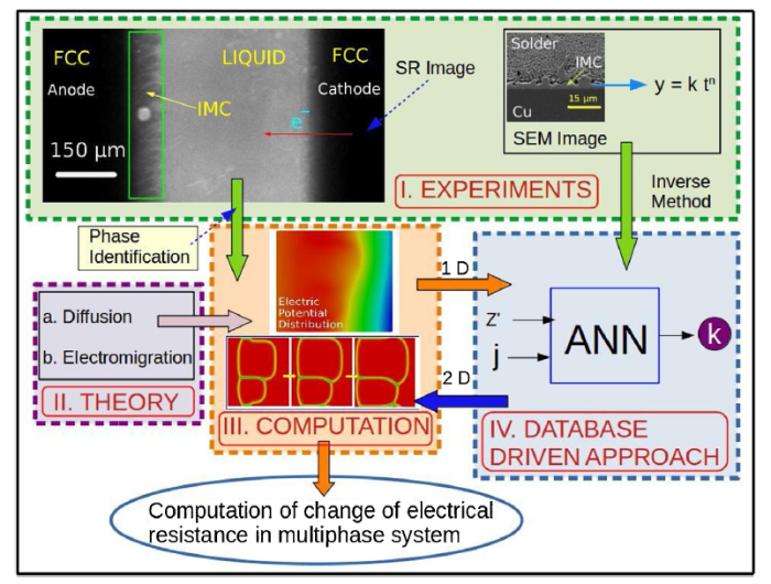
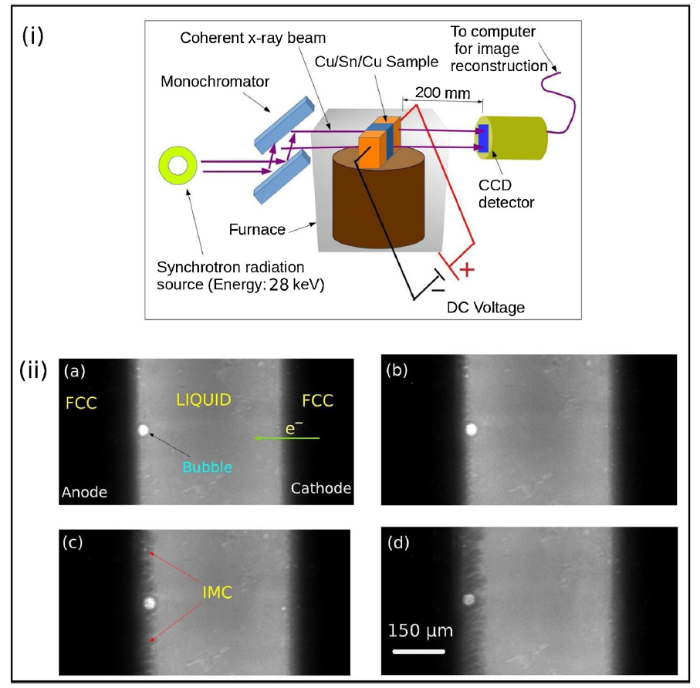
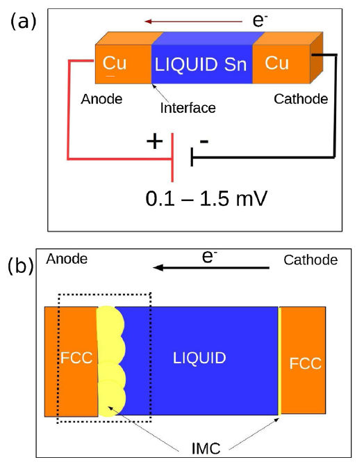
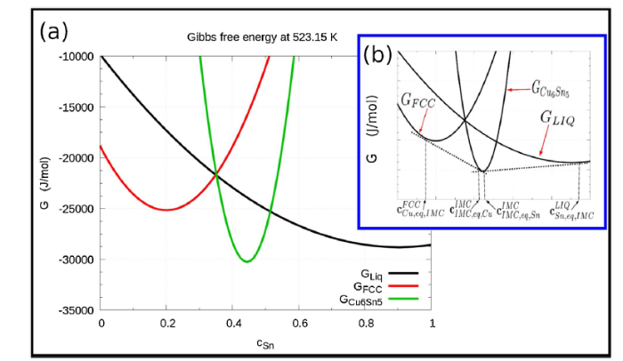
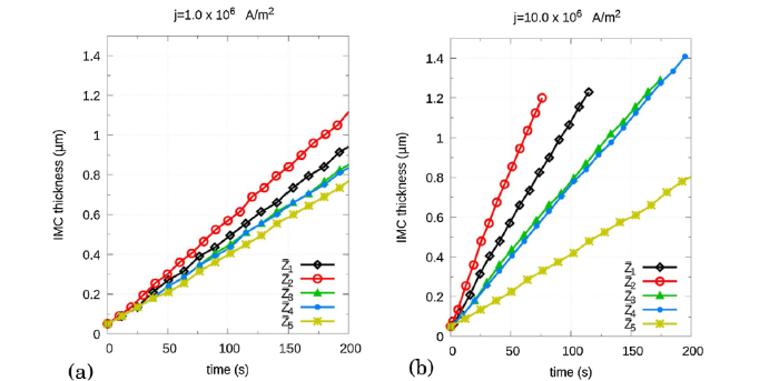
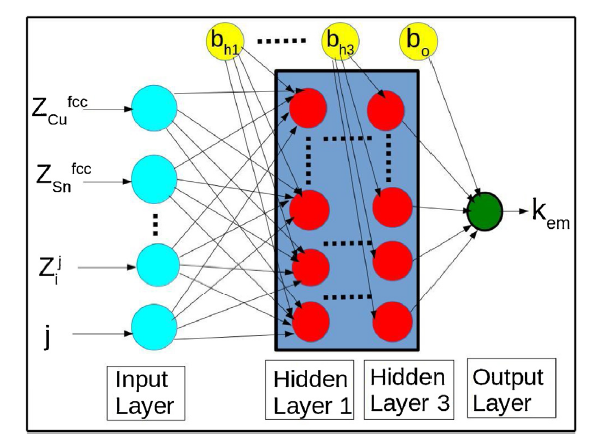
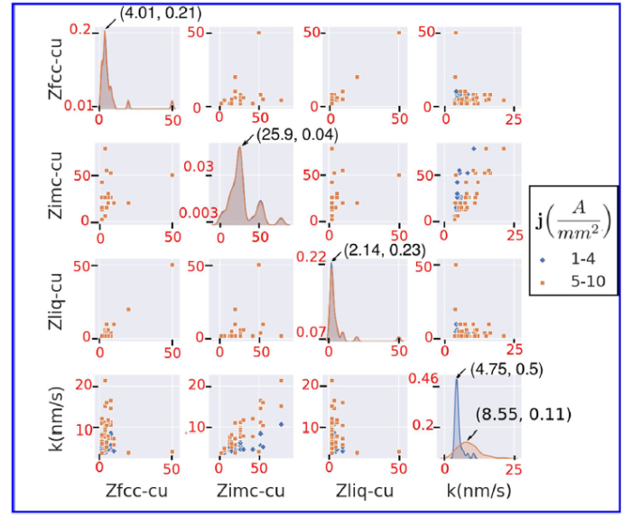

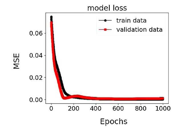
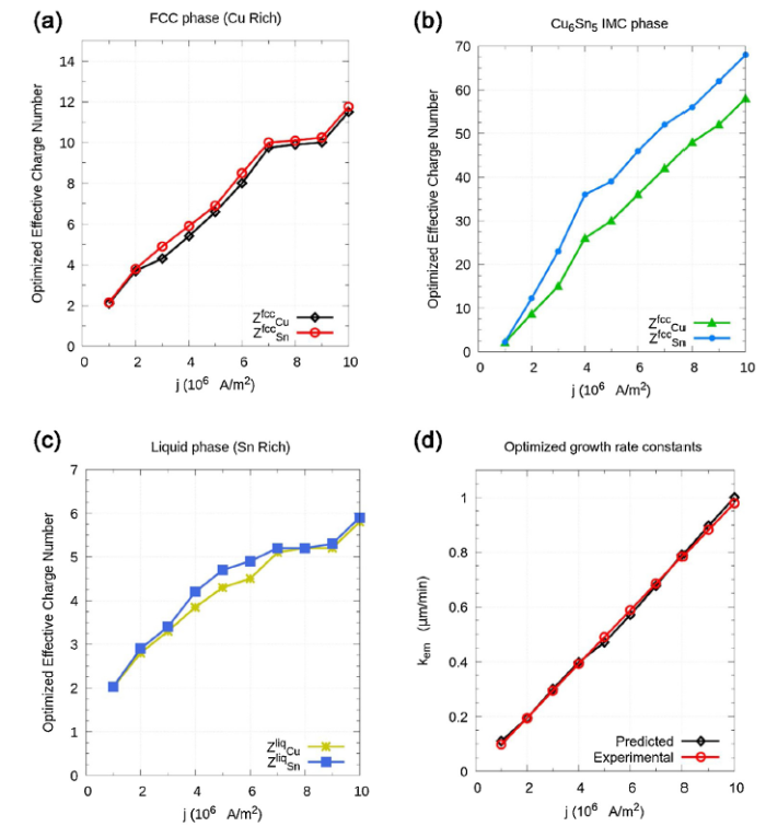
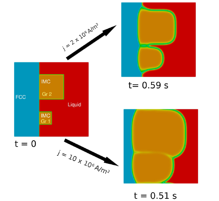
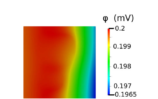
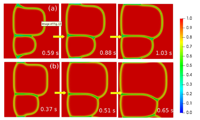
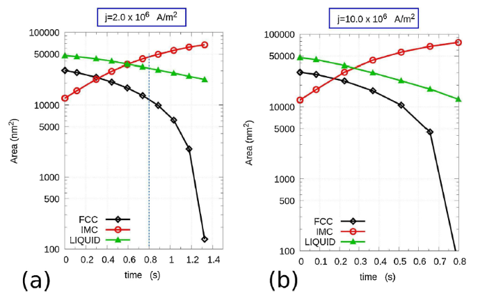


 WeChat