
Characterization of Microstructural and Morphological Properties in As-deposited Ta/NiFe/IrMn/CoFe/Ta Multilayer System
[Öksüzoğlu Ramis Mustafa1, *  , Sarac Umut
2 , Yıldırım Mustafa1 , Çınar Hakan1 ]
, Sarac Umut|
|


Surface morphology and its relationship with microstructure in Ta/NiFe/IrMn/CoFe/Ta multilayer system deposited by pulsed DC magnetron sputtering have been investigated in dependence of Ta buffer and NiFe seed layer thicknesses using atomic force microscopy. The structural parameters such as grain size, dislocation density, texture and strain were calculated. For each surface, a self-affinity behavior with mean fractal dimensions in the range of 2.03–2.18 was found. Additionally, it was also observed that the surface of all samples has locally smooth textured surface structure in the short range. The texture aspect parameter and texture direction index have been obtained for isotropy/anisotropy surface texture. A significant relationship between the surface texture and the strength of the <111> texture in IrMn layer has been found. The analysis indicated that the surface roughness is strongly affected by the thicknesses of the NiFe seed and Ta buffer layers.
Exchange bias (EB) systems in spin valves have been widely investigated due to their applications in magnetic recording heads and magnetic sensors [1], [2] and [3]. In spite of wide range applications, considerable research is still ongoing to find optimal materials for the antiferromagnetic layer and suitable under layers (ULs) such as buffer and seed layers [1], [2] and [3]. Magnetic properties were generally correlated with the <111> out-of-plane texture [4] developing with ULs and consequently the choice of ULs for the deposition of antiferromagnetic (AF) layer becomes crucial. In addition to that it is necessary to understand the evolution of microstructure (i.e. roughness, texture, strain, grain size etc.), especially in the as-deposited state, in order to optimize the growth conditions of spin valve sensor elements. Atomic force microscopy (AFM) is a powerful tool not only to study the amplitude parameters such as the root mean square (RMS) and average roughness, and it can also be used to investigate spatial parameters such as mean fractal dimension, texture direction index and texture ratio aspect parameter [5], [6], [7], [8] and [9]. These roughness parameters were investigated in different thin film systems grown with various deposition techniques and applications [5], [6], [10], [11], [12] and [13]. However, to our best knowledge, in the AF IrMn based EB systems, there is no work about the variation of roughness parameters as a function of ULs. In the present study, the influence of Ta/NiFe ULs on roughness parameters and their correlations to the microstructural properties have been investigated for the pulsed DC magnetron sputtered Ta/NiFe/IrMn/CoFe/Ta multilayer system in the as-deposited state.
Two series of Ta/Ni81Fe19/Ir20Mn80/Co90Fe10/Ta multilayer system were prepared onto Si/1000 nm thermal SiO2 substrates using the pulsed DC magnetron sputtering technique at Ar gas pressure of 2–3 mTorr (0.267–0.4 Pa) and without substrate heating, resulting in the following layer sequences: Ta (5 nm)/Ni81Fe19( ts)/Ir20Mn80 (10 nm)/Co90Fe10 (2 nm)/Ta (5 nm) with different thicknesses of NiFe seed layer ts = 2, 4, 6, 8 and 10 nm called in the present work as S1 and Ta( tb)/Ni81Fe19 (8 nm)/Ir20Mn80 (10 nm)/Co90Fe10 (2 nm)/Ta (5 nm) with different thicknesses of Ta buffer layer tb = 2, 4, 6, 8 and 10 nm called as S2. The base pressure prior to the deposition was on the order of 2 × 10⁻⁹ Torr (267 × 10-9 Pa). The purity and the composition of target materials were 99.95% pure NiFe-81/19 at.%, 99.95% pure CoFe-90/10 at.% and 99.9% pure IrMn-20/80 at.% (Kurt J. Lesker Company). Each set of specimens was grown during the same vacuum cycle. The X-ray reflectivity technique was used for calibration of deposition rate for each layer and the deposition time was kept constant for desired layer thicknesses. The morphological characteristics of samples were studied by AFM (Veeco Multimode 5) in tapping mode under ambient pressure and temperature in as-deposited state. AFM images were taken immediately after the sample production, in order to avoid possible oxidation of sample surfaces. Quantitative analyses of roughness parameters of both sample series have been carried out by means of Scanning Probe Image Processor (SPIP) from Image Metrology Incorporation available on [14]. Crystallographic structure of the samples in the as-deposited state was analyzed by X-ray diffraction (XRD) technique. XRD patterns were collected using a Bruker 4-circle diffractometer equipped with a Cu sealed tube point source and a Göbel Mirror optic to generate a 2D-collimated parallel beam (divergence ca. 0.03° and a lateral length of 18 mm) and an anti-scatter slit to remove background arising from small 10 mm × 10 mm square samples.
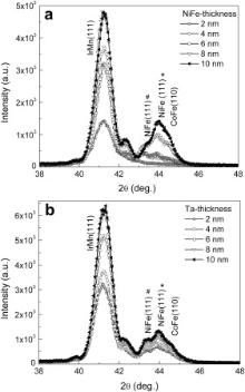
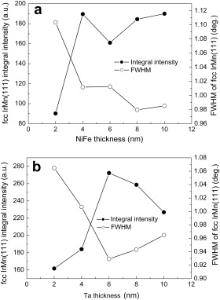
XRD patterns of the S1 and S2 samples in as-deposited state are shown in Fig. 1(a) and (b), respectively. XRD patterns indicate the face centered cubic (fcc) structure of IrMn(111), fcc NiFe(111), and body centered cubic (bcc) CoFe(110). Two diffraction peaks can be attributed to Awaruite-Ni81Fe19 permalloy (NiFe(111)* in Fig. 1(a) and (b)) and to Taenite-Ni50Fe50 (NiFe(111)# in Fig. 1(a) and (b)). In both samples, diffraction peak from Ta layers was not observed, which can be explained most probably by nano-crystalline or amorphous Ta layer. In both S1 and S2 samples, the intensity of the IrMn (111) peak is influenced by the thickness of the Ta/NiFe layers ( Fig. 1(a) and (b)), which indicates also that the preferred <111> orientation (i.e. texture) of the IrMn layer depends on the thickness of the Ta/NiFe ULs. The integral intensity and the full width at half maximum (FWHM) of the diffraction peaks can give information on the evolution of the degree of the texture. The lowest FWHM together with the highest integral intensity is a measure for the strength of texture. The integral intensity and the FWHM values of the IrMn(111) diffraction peak were obtained by the peak profile fitting for both S1 and S2 sample series; Fig. 2(a) and (b) indicate the evolution of the integral intensity and the FWHM values as a function of the thickness of the Ta/NiFe layers. As shown in Fig. 2(a), the integral intensity of the IrMn(111) peak increases up to NiFe seed layer thickness of 4 nm and remains nearly constant except from the value for the NiFe thickness of 6 nm. The FWHM values decrease with increasing NiFe thickness up to 8 nm and remain almost constant. According to these results, the degree of the <111> out-of-plane texture in IrMn layer can be achieved first for the NiFe thickness of 4 nm. It becomes stronger up to the NiFe seed layer thickness of 8 nm and finally tends to saturate at 10 nm.
 | Fig. 1. XRD patterns of (a) Ta (5 nm)/NiFe ( ts = 2–10 nm)/IrMn(10 nm)/CoFe (2 nm)/Ta (5 nm) and (b) Ta ( tb = 2–10 nm)/NiFe (8 nm)/IrMn (10 nm)/CoFe (2 nm)/Ta (5 nm) samples as a function of the NiFe seed and Ta buffer layer thicknesses. |
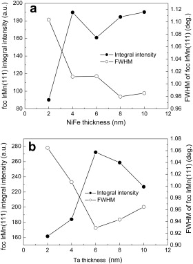 | Fig. 2. Evolution of the integral intensity and the FWHM values of the fcc IrMn (111) peak, (a) as a function of the thickness of the NiFe seed, (b) Ta buffer layers. All lines are guide for the eye. |
On the other hand, the integral intensity of IrMn(111) peak for different Ta layer thicknesses increases up to 6 nm and then decreases, whereas the FWHM values show an opposite tendency ( Fig. 2(b)). The highest integral intensity and the lowest FWHM for the Ta buffer layer thickness of 6 nm reflect the highest degree of the <111> out-of-plane texture. Consequently, a reasonable degree for the <111> texture in the IrMn layer have been found for the Ta/NiFe thickness combinations; Ta (6 nm)/NiFe (8 nm), Ta (5 nm)/NiFe (8 nm) and Ta (5 nm)/NiFe (10 nm) in the as-deposited state of samples.
In order to study the evolution of the grain size, dislocation density and strain, and their correlations, the average grain size of AF IrMn layer, D, was calculated from FWHM of fcc IrMn (111) peak using the Scherrer formula [15]:
where θ is the Bragg's angle. Additionally, the strain, ɛ, in the IrMn layer was calculated from the XRD patterns using the relation [16]:
and ɛ values are found to be in the range of (4.001–4.508) × 10−3 lines−2 m−4 and (3.796–4.349) × 10−3 lines−2 m−4 for S1 and S2 samples, respectively. Fig. 3(a) and (b) indicate the variation of the strain and grain size with the thickness of the NiFe seed and Ta buffer layers, respectively. As shown in Fig. 3, lower ɛ values have been found for the samples with Ta/NiFe layer thickness combinations: Ta (5 nm)/NiFe (8 nm), Ta (5 nm)/NiFe (10 nm) and Ta (6 nm)/NiFe (8 nm). In addition to that, a direct correlation between the grain size and strain in the IrMn layer was observed, which develops with the thickness of the Ta buffer and NiFe seed layers, i.e., the higher (lower) the strain, the smaller (larger) the grain size. Similar results were found for electrodeposited Ni [17] and Ni–Cu films [18] and chemical bath deposited cadmium selenide thin films [19]. Furthermore, the results also indicate a direct correlation between the degree of the <111> texture and average grain size in the IrMn layer developing with the thickness of the Ta buffer and NiFe seed layers, i.e., the higher (lower) the degree of <111> texture, the larger (smaller) the grain size.
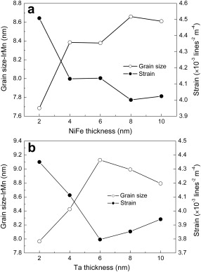 | Fig. 3. Variation of the strain and grain size (a) as a function of the NiFe seed, (b) Ta buffer layers thicknesses. All lines are guide for the eye. |
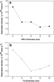
The dislocation density ( δ) was estimated using Williamson and Smallman& formula [20]:
where n is a factor, which is unity for thin films [21]. The estimated δ values are in the range of (1.3335–1.6932) × 1016 lines m-2 and (1.2001–1.5759) × 1016 lines m-2 for S1 and S2 samples, respectively. The evolution of δ values as a function of the thickness of the NiFe seed and Ta buffer layers are shown in Fig. 4(a) and (b), respectively. As seen from Fig. 4, the lower δ values in IrMn layer have been found in the Ta (5 nm)/NiFe (8 nm), Ta (5 nm)/NiFe (10 nm), and Ta (6 nm)/NiFe (8 nm) samples.
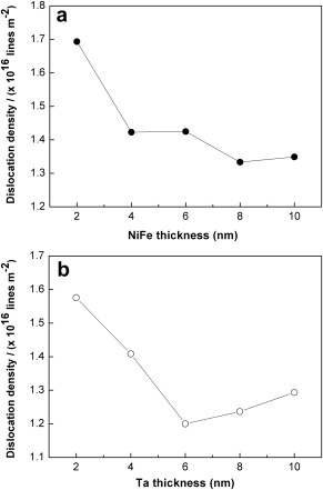 | Fig. 4. Variation of the dislocation density (a) as a function of the NiFe seed, (b) Ta buffer layers thicknesses. All lines are guide for the eye. |
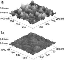
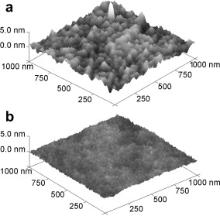
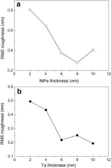
In order to investigate the evolution of roughness parameters as a function of the NiFe seed and Ta buffer layer thicknesses, AFM measurements were performed. As an example, AFM images for S1 (NiFe thicknesses of 2 and 8 nm) and S2 samples (Ta thicknesses of 2 and 6 nm) are shown in Fig. 5 and Fig. 6, respectively. AFM images indicate that surfaces of S1 and S2 samples are covered with small grains of different sizes. On the other hand, it can be clearly seen that the samples with NiFe ( Fig. 5(a)) and Ta ( Fig. 6(a)) thickness of 2 nm have larger grains than the other samples with NiFe thickness of 8 nm ( Fig. 5(b)) and with Ta thickness of 6 nm ( Fig. 6(b)). Firstly, the value of RMS roughness for each surface was obtained. The evolution of the RMS roughness as a function of the thickness of the NiFe seed and Ta buffer layers is given in Fig. 7(a) and (b), respectively. In the S1 samples, the RMS roughness decreases up to 8 nm and then increases ( Fig. 7(a)). The lowest RMS roughness is achieved for the NiFe layer thickness of 8 nm. However, in the S2 samples, the RMS roughness reduces with increasing Ta buffer layer thickness up to 6 nm and then remains almost constant ( Fig. 7(b)). In comparison between the S1 and S2 samples, surface roughness values are lower in the S2 samples, which can be explained by the optimum NiFe layer thickness of 8 nm in the S2 samples. In general, the variation of the strain ( Fig. 3) and the dislocation density ( Fig. 4) as a function of Ta/NiFe UL thicknesses are considered; it can be clearly seen that the samples with smaller RMS roughness have smaller strain and dislocation density.
 | Fig. 5. AFM topographic images of S1 samples with the thickness of the NiFe seed layer: (a) 2 nm, (b) 8 nm (scan scale of 1 μm × 1 μm). |
 | Fig. 6. AFM topographic images of S2 samples with the thickness of the Ta buffer layer: (a) 2 nm, (b) 6 nm (scan scale of 1 μm × 1 μm). |
 | Fig. 7. Evolution of the RMS surface roughness as a function of the NiFe seed (a), and Ta buffer layers thicknesses (b). All lines are guide for the eye. |
Furthermore, the values of the fractal dimension in S1 and S2 samples were calculated using the software SPIP, in order to investigate the self-affinity of all surfaces. The fractal dimension is calculated at different angles by analyzing the Fourier amplitude spectrum. In this study, we present only the mean fractal dimension, D, which is defined as an average for all directions. The D parameters obtained for S1 and S2 samples are given in . In all S1 and S2 samples, the D parameter was found to be in the range of 2.03–2.18, which indicates self-affined surfaces. The Hurst parameter, H, is directly related to the D parameter by the following relation D = 3 - H [3], [22] and [23]. A larger value of H (>0.5) corresponds to a locally smooth textured surface structure in the short range, while small values of H describe (<0.5) more locally jagged surface [12], [13], [24], [25] and [26]. The values of H parameter obtained for S1 and S2 samples are also listed in . Since H parameter was found to be greater than 0.5 in all S1 and S2 samples, it can be concluded that the surface of all S1 and S2 samples has locally smooth textured surface structure in the short range.
| Table 1. Mean fractal dimension D and Hurst parameter H values of investigated S1 and S2 samples |
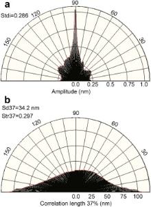
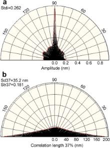
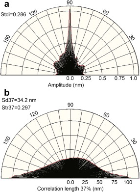
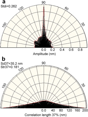
A study with using SPIP™ software package has been performed in order to investigate the isotropy/anisotropy of surfaces of all samples. From the angular spectrum, the texture direction index, Stdi, was calculated (shown in Fig. 8 and Fig. 9 for the S1 sample with NiFe thickness of 8 nm and for the S2 sample with Ta thickness of 6 nm, respectively). In , the Stdi values are given with respect to NiFe and Ta thicknesses. Surfaces with very dominant directions have Stdi values close to 0 and Stdi values close to 1 indicate that the amplitude sum of all direction are similar, i.e., no dominant direction exists [27]. Since Stdi parameter was found to be greater than 0.5 for 2 nm thickness of NiFe and Ta layers, it can be assumed that the amplitude sum of all directions is similar, i.e., the surface texture of these samples seems to be isotropic [11]. In contrast to that, Stdi values are lower than 0.5 for the NiFe and Ta thicknesses over 2 nm. Accordingly, smaller Stdi values found in the S1 samples with NiFe thicknesses of 8 and 10 nm and with Ta thickness of 6 nm indicate an anisotropic surface texture.
 | Fig. 8. Angular AFM spectrum for the S1 sample with NiFe layer thickness of 8 nm: (a) amplitude, (b) correlation length plot. |
 | Fig. 9. Angular AFM spectrum for the S2 sample with Ta layer thickness of 6 nm: (a) amplitude, (b) correlation length plot. |
| Table 2. Texture direction index Stdi and texture aspect ratio Str37 values of investigated S1 and S2 samples |
The texture ratio aspect parameter, Str37, obtained from the correlation length plot (shown in Figs. Fig. 8 and Fig. 9 for S1 sample with NiFe thickness of 8 nm and S2 sample with Ta thickness of 6 nm, respectively) could be used to identify the texture strength [11]. Str37 is also called as the isotropy index, which describes the degree of isotropy of the surface texture [27]. It is defined as the ratio of the fastest to slowest decay to 37% of the autocorrelation function. A strong anisotropic surface has an Str37 value close to 0, whereas a spatially isotropic surface has a Str37 value close to 1 [11] and [27]. The Str37 values obtained for S1 and S2 samples are also given in . The Str37 values were found to be greater than 0.5 for NiFe and Ta thicknesses of 2 nm, which reflect a spatially isotropic surface texture [11]. The values of Str37 parameter become lower than 0.5 for the NiFe and Ta thicknesses over 2 nm, except from NiFe thickness of 6 nm. Thus, it can be suggested that the surface texture of the sample with NiFe thickness of 6 nm seems to be isotropic. And, lower Str37 values estimated for NiFe thicknesses of 8 and 10 nm, and Ta thickness of 6 nm indicate a stronger anisotropic surface texture.
As a result, the Ta (6 nm)/NiFe (8 nm), Ta (5 nm)/NiFe (8 nm) and Ta (5 nm)/NiFe (10 nm) samples have stronger degree of the anisotropic surface texture in comparison to other samples. As given in the XRD results, these samples have also stronger degree of <111> texture in the IrMn layer. On the other hand, the lowest degree of <111> texture in IrMn layer has been found in Ta (5 nm)/NiFe (2 nm) and Ta (2 nm)/NiFe (8 nm) samples, which exhibit spatially isotropic surface texture. Accordingly, it can be concluded that there is a direct correlation between degree of isotropy/anisotropy of the surface texture and <111> texture strength in IrMn layer developing with Ta buffer and NiFe seed layer thicknesses.
The morphological and microstructural differences in two series of as-deposited Ta/NiFe/IrMn/CoFe/Ta multilayer system have been investigated depending on NiFe seed and Ta buffer layer thicknesses. From the structural analysis, it was found that the Ta (6 nm)/NiFe (8 nm), Ta (5 nm)/NiFe (8 nm) and Ta (5 nm)/NiFe (10 nm) samples have smaller dislocation density and strain, higher degree of the <111> texture, and larger grain size in IrMn layer. AFM images of the as-deposited multilayer films revealed that the surface roughness is significantly influenced by the ULs thicknesses. Furthermore, AFM studies also indicated that the surface of all samples possesses smooth textured surface structure in the short range. All surfaces are characterized by self-affinity with mean fractal dimension in the range of 2.03–2.18. No preferential dependency of the surface texture for the Ta (5 nm)/NiFe (2 nm) and Ta (2 nm)/NiFe (8 nm) samples was observed. Furthermore, in these samples, the lowest degree of the <111> texture in IrMn layer has been found. In addition to that, a stronger degree of the anisotropic surface texture and a higher degree of the <111> texture in the IrMn layer have been found for the Ta/NiFe thickness combinations of Ta (6 nm)/NiFe (8 nm), Ta (5 nm)/NiFe (8 nm), and Ta (5 nm)/NiFe (10 nm). Accordingly, it can be concluded that there is a direct correlation between the degree of isotropy/anisotropy of the surface texture and the strength of the <111> texture in the IrMn layer, which develops with the thickness of the Ta buffer and NiFe seed layers. Accordingly, the present study revealed that the microstructural and morphological properties of the as-deposited Ta/NiFe/IrMn/CoFe/Ta multilayer system are significantly affected by the thicknesses of Ta/NiFe under layers.
This work was partially supported by TUBITAK under Grant No. MAG-106M517, the Directorate for Scientific Research Projects of Anadolu University under Grant No. BAP-050255 and the DPT (State Planning Organization of Turkey) through Project No. DPT-2004-06.
| 1. |
|
| 2. |
|
| 3. |
|
| 4. |
|
| 5. |
|
| 6. |
|
| 7. |
|
| 8. |
|
| 9. |
|
| 10. |
|
| 11. |
|
| 12. |
|
| 13. |
|
| 14. | [Cited within: 1] |
| 15. |
|
| 16. |
|
| 17. |
|
| 18. |
|
| 19. |
|
| 20. |
|
| 21. |
|
| 22. |
|
| 23. |
|
| 24. |
|
| 25. |
|
| 26. |
|
| 27. |
|