
Thermal Stability of ALD Lanthanum Aluminate Thin Films on Si (100)
[She Xiaofeng, Wang Hongtao*  ]
]
]
|
|


The thermal stability of high-κ dielectrics on Si is critical in avoiding the malfunction of metal oxide field effect transistors (MOSFET) in devices. Series of annealing experiments have been performed to investigate the thermal stability of atomic layer deposited (ALD) lanthanum aluminate (LAO) thin films, a promising amorphous high-κ candidate. The abrupt interface between LAO and Si remains intact at temperatures below 600 °C. Above this temperature, a SiO2-rich interfacial layer begins to appear and thickens at higher temperatures. At 900 °C, the interface is roughened due to the formation of nano sized crystal nuclei above the interfacial layer, which indicates the interfacial reactions with the Si substrate. The thermal stability of ALD Al2O3 thin films on Si have also been studied under similar conditions. The Al2O3/Si interface retains its smoothness even after full crystallization. This comparison suggests that the rare earth element may catalyze the interfacial reactions. Further annealing experiments on LAO films with different thickness and with a capping layer show that the oxygen source of the interfacial layer mainly comes from the ALD oxide films.
The thermal stability of a high-κ dielectric in direct contact with Si substrate has attracted much attention because the electronic transport is sensitive to any microstructure change in devices [1]. The thermal stability of binary metal oxide ( MO x) on Si was evaluated by considering the following reactions in a typical process temperature range of 300–1300 K [1]:
Si+MOx→M+2SiO (1a)
Si+MOx→MzSi+2SiO (1b)
Si+MOx→M+MySiOz (1c)
If the Gibbs free energy (Δ G0) for any of the above reactions is less than zero at certain process temperature, the MO x/Si system is regarded to be thermally unstable. This method successfully excluded many oxides as gate dielectrics. But it still left some practical questions open: (1) The thermal stability of amorphous metal oxides/Si system. This question arises naturally because some important high-κ oxides are amorphous such as lanthanum aluminate (LAO). (2) The thermal stability of ternary metal oxides/Si system. (3) The source of oxygen for the formation of SiO2-rich interfacial layer.
There is no general method in tackling these questions due to the varieties in the thin film deposition and annealing process. In this work, we focus on the microstructure evolution of two important atomic layer deposited (ALD) high-κ oxides, aluminum oxide (Al2O3) and lanthanum aluminate (LaAlO3), vs temperatures, which may shed light on the annealing behavior of amorphous high-κ oxides on Si.
Lanthanum aluminum oxide thin films were deposited in a home-built flow-type reactor operated at the base pressure of 300 mTorr (~40 Pa) and 300 °C with the precursors of lanthanum tris(isopropyformamidinate), trimethylaluminum (TMA) and H2O. The lanthanum precursor was kept at 120 °C in the oven and TMA and H2O at room temperature. The composition of the as-deposited LAO film on the glassy carbon substrate (Alfa Aesar® brand) was La1.1Al0.9O3 when the pulse ratio of the lanthanum precursor to TMA was 2:1, which was determined by Rutherford backscattering spectrometry (RBS) measurements. For the light element, especially carbon, impurity peaks are overwhelmed by the substrate carbon tail. Auger was thus used to detect the carbon concentration. After surface cleaning by Ar+ sputtering, no C or N impurities were detected. The C concentration decreased with sputtering time and reached the detection limit of the Auger instrument.
The films were grown on single-side polished, n-type phosphor-doped (100) silicon wafer with resistivity of 5–10 Ω cm. Prior to transferring to the reactor, the substrate was sonicated in organic solvents, i.e. acetone, methanol and isopropanol, in sequence for 3 min each. Then it was dipped into dilute hydrofluoric acid for 10 s and rinsed with de-ionized water. After deposition, the sample was quickly transferred to an Inconel-tube furnace under ultra-high purity argon gas purging at 200 mTorr (26.7 Pa). Right at the inlet of the furnace tube, a Mykrolis™ purifier was used to minimize the effect of oxygen and water from the environment. The samples were annealed at temperatures from 500 to 900 °C at an interval of 100 °C. The holding time at the temperature was 1 min for all samples. The temperature ramping rate was approximately 60 °C/min. Before annealing, the system had been purged for at least 30 min.
Cross-sectional transmission electron microscopy (TEM) was used to investigate the microstructure evolution with increasing annealing temperatures. X-ray diffraction (XRD) and the plane-view TEM were used to characterize the structure of the crystallized LAO films after annealing. High-angle annular dark field scanning transmission electron microscopy (HAADF-STEM) was employed to study the composition redistribution during crystallization. Finally X-ray reflectivity (XRR) was used to quantitatively measure the film thickness and interface roughness variation.
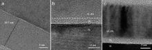
Fig. 1(a) shows the cross-sectional TEM image of the as-deposited La1.1Al0.9O3 film on Si. The film is amorphous, as revealed by the random patterns. The interface is atomically abrupt under the deposition condition. When samples were annealed in the Inconel-tube furnace, a uniform interfacial layer (IL) began to be observed at 600 °C. Estimated from the mass contrast difference in high resolution transmission electron microscopy (HRTEM) images, the IL thickness was found to be 1.5 ± 0.5 nm at 600 °C, 3.9 ± 0.4 nm at 700 °C and 4.0 ± 0.4 nm at 800 °C ( Fig. 1(b–d)) for a 12 nm La1.1Al0.9O3 film on Si (100).
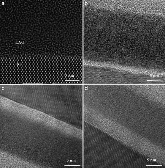 | Fig. 1. (a) Cross-sectional TEM image of an as-deposited La1.1Al0.9O3 film on Si; Cross-sectional TEM images of La1.1A0.9O3 films on Si (100) substrates after annealing for 1 min at (b) 600 °C, (c) 700 °C and (d) 800 °C. |
For comparison, annealing experiments were done for 20 nm ALD Al2O3 films with precursors of TMA and H2O. The as-deposited Al2O3 is uniform and has sharp interface with Si substrate ( Fig. 2(a)). The annealing temperature varies from 450 to 900 °C. A 1.2 ± 0.6 nm thick IL is firstly observed at 600 °C ( Fig. 2(b)). At elevated temperature, the IL grows thicker. It is 1.5 ± 0.2 nm for 750 °C and 2.6 ± 0.3 nm for 900 °C ( Fig. 2(c)), which is consistent with the post annealing of a similar system studied by Katamreddy et al. [2] and [3]. From this comparison, it comes to the conclusion that the IL growth is enhanced by the addition of the rare earth element lanthanum. Excluding the effect from the ambient oxygen, this enhancement may be the consequence of three factors: (1) lanthanum oxide reacts with water so that more hydroxide groups are trapped in the LAO film than the aluminum oxide film; (2) lanthanum catalyzes the oxidation of silicon surface; (3) rare earth oxides are good oxygen ion conductors.
 | Fig. 2. (a) Cross-sectional TEM image of Al2O3/Si sample after annealing at 450 °C; Cross-sectional TEM images of Al2O3/Si samples after annealing at (b) 600 °C and (c) 900 °C. |
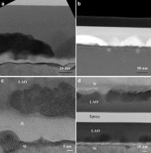
Both LAO and Al2O3 films crystallize at 900 °C. The IL between polycrystalline Al2O3 film and Si is uniform after crystallization ( Fig. 2(c)). In contrast, rather rough Si surface ( Fig. 3(a)) is observed in the LAO/Si system after annealing at 900 °C, which is an evidence of intensive reactions or Si atoms migration. Most of the nuclei are found right above the amorphous IL. Composition redistribution can be observed in the HAADF-STEM image ( Fig. 3(b)), where the darker area is rich of light elements and therefore has less density ( ρ). It is easy to see ρcrystal> ρLAO> ρSi> ρIL. As it is shown that the significant Si atoms are incorporated into the LAO film, it is likely that both the crystals and IL are silicate with different percentage of SiO2 ( Fig. 3(c, d)). The crystals are La2O3-rich while the IL is SiO2-rich.
 | Fig. 3. (a) Cross-sectional TEM image and (b) HAADF-STEM image of the annealed (900 °C, 1 min) La1.1Al0.9O3 film on Si, (c) HRTEM image of the interfacial layer, (d) low magnification TEM image. |
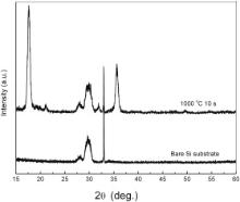
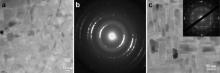
The crystallized films were analyzed by XRD ( Fig. 4). The peak positions cannot match any of the known crystalline structures of lanthanum aluminate, silicide or silicate in the database of ICDD-PDF (2003). Since stable La–Al–Si–O phases exist [4] and reactions between the film and Si are clearly observed in Fig. 3(a, b), the crystals may be one of quaternary elements phases. Unfortunately, a few XRD spectra were reported for these phases. In Ref. [5] and [6], the crystal structure was clearly identified as LaAlO3 after annealing 100 nm molecule-beam-deposited amorphous LAO films at both 940 and 1040 °C. This difference may be due to the different film thickness and stoichiometry. The crystal shape is shown in plane-view TEM images. For samples annealed at 900 °C, the nuclei have the equal-axis shape ( Fig. 5(a)). Strong texture is observed by the selected area electron diffraction (SAED) ( Fig. 5(b)). When fully crystallized at 1000 °C, the grains are elongated along certain crystal direction and accommodated to each other perpendicularly or in parallel ( Fig. 5(c)). The texture is further developed into epitaxial relation to the Si, which is also verified by SAED pattern in the inset of Fig. 5(c).
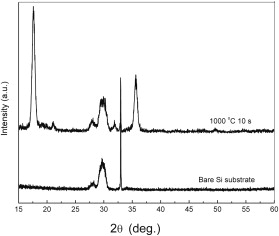 | Fig. 4. XRD patterns of the sample the sample annealed at 1000 °C for 10 s in the N2 environment and the bare substrate. |
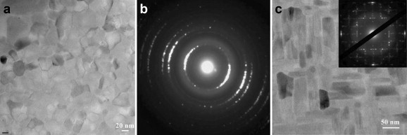 | Fig. 5. (a) Plane-view TEM image of the film annealed at 900 °C, (b) corresponding SAED pattern, (c) plane-view TEM image of the sample annealed at 1000 °C for 10 s in the N2 environment. The inset is the corresponding SAED pattern of Fig. 5(c). |
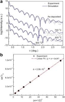
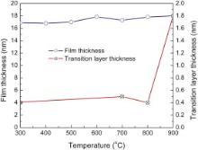
The interfacial layer thickness vs annealing temperature was measured by XRR ( Fig. 6(a)). By relating the local maxima position to its order, the film thickness can be extracted ( Fig. 6(b)), which is consistent with the cross-sectional TEM observations (not shown). The results are summarized in Fig. 7. The LAO film thickness slightly increases from 17 to 18 nm as the annealing temperature is increased to 900 °C. Though an IL was readily observed in samples annealed at temperatures above 600 °C, this structure is not resolved by the XRR profile in Fig. 6(a, b). The inability of XRR to resolve the IL implies that the IL has similar density to Si substrate since XRR spectra depend on the density ratio profile of the multilayer to the Si substrate. This observation is consistent with the HAADF-STEM image in Fig. 3(b), where the IL is only slightly darker than Si substrate. The XRR spectra could be well fitted by modeling the system as a stack of LAO film/transition layer (TL)/substrate (both the IL and Si) with the TL introduced to account for the interface roughness or intermixing. The TL thickness is kept constant (∼0.4 nm) during annealing up to 800 °C, which is in the order of the Si surface roughness (TL thickness = 2 × RMS roughness). At 900 °C, the TL thickness abruptly increases to 1.8 nm, which confirms that substantial diffusion occurs near the interface.
 | Fig. 6. (a) XRR measurements of annealed samples and simulation, (b) an example showing how the film thickness was extracted from the XRR spectrum. |
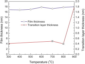 | Fig. 7. Film thickness and the transition layer thickness variation with annealing temperatures. |
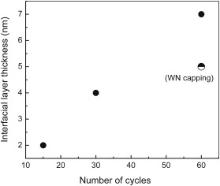
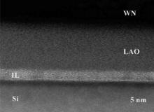
The growth of the interfacial layer needs oxygen source, which can be supplied by the annealing ambient, the film itself or a combination of the two. If oxygen diffusion through the film is the dominant mechanism, a thicker film will slow down the diffusion of oxygen to the interface and therefore a thinner IL will be expected. Fig. 8 summarizes the results of a series of annealing experiments by varying the film thickness. All the annealing experiments were done under ultra-high purity argon gas purging at 200 mTorr (26.7 Pa) at 800 °C for 1 min. The IL thickness was measured by cross-sectional TEM and almost linearly proportional to the film thickness, which proves that the oxygen source mainly comes from the film itself. In order to minimize the effect of possible residue oxygen in the purified Ar purging gas, a 25 nm WN film was deposited on the top of a 15 nm La1.1Al0.9O3 film ( Fig. 9) in the same reactor with bis(tertbutylimido)bis(dimethylamido) tungsten and ammonia [7] and [8]. WN was chosen because it has good diffusion barrier property and is relatively easy to be oxidized. A 5 nm IL was observed under the same annealing condition, which confirmed the source of oxygen resides in the film. The IL thickness reduction from 7 to 5 nm ( Fig. 8) may be due to the oxidation of the WN capping.
 | Fig. 8. Relation between the interfacial layer thickness and the LAO film deposited with different ALD cycles. |
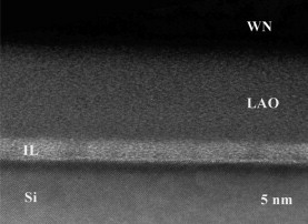 | Fig. 9. Cross-sectional TEM image of WN/La1.1Al0.9O3/Si sample after annealing at 800 °C. |
The observation of IL was also carried out in high-κ films deposited with either PVD [9], [10], [11], [12], [13] and [14] or ALD [15], which have negative Gibbs free energies for the reactions (, and ) and thus are considered to be thermally stable on Si. However, caution must be taken in applying the thermal equilibrium arguments.
(1)Thermal equilibrium. This requirement can hardly be met in a thin film system with thickness of 5–100 nm. An amorphous film is not in its thermal equilibrium phase.
(2)Interface and surface. For films with thickness in the order of 10 nm, both interface and surface regions are substantial parts of the film, which may not have the same property as the “bulk”.
(3)Stoichiometry. Multi-component thin films do not have the same stoichiometry as their bulk counterpart. For CVD or ALD, stoichiometry relies on both precursors and deposition condition.
The differences of thin films from bulk materials make the thermal equilibrium argument be a necessary condition instead of a sufficient criterion. Any conclusion of the thermal stability must come from the microstructure study instead of any plausible thermodynamic argument.
Due to the importance of thermal stability of ALD dielectric on Si, great efforts have been made to stabilize the oxide/Si interface [16], [17], [18], [19], [20], [21], [22], [23], [24] and [25]. Most of the work has uncovered the electrical deterioration at elevated temperatures, which are in a range of 600–900 °C and depend specifically on the detailed processing condition, chemical composition and structure of the ALD thin films. A few of them studied the microstructure evolution with temperature. However, a thorough literature survey shows that the oxygen source of the interfacial layer mainly comes from the non-stoichiometry of ALD oxides [16], [17], [18], [19], [20], [21], [22], [23], [24], [25], [26], [27], [28], [29] and [30], which agrees with our study on the capped oxide films. Therefore, changing the thin film structure, such as using laminated film stacks, cannot effectively suppress the growth of interfacial layer [21]. An interfacial barrier layer, such as a sub-1-nm SiO2 can slow down the oxygen diffusion from the ALD thin film to the Si substrate. It is noted that the as-grown SiO x interfacial layer is not an effective barrier, which is supposed not as dense as the thermally grown SiO2 at high temperature and with sufficient oxygen supply. We expect that even a very thin thermally grown SiO2 can also suppress the Si diffusion, and therefore delay the formation of silicides. In this way, the interface stability can be further improved. The role of pre-grown SiO2 in stabilizing the interface needs further investigation.
The microstructure evolution of ALD LAO films on Si was characterized. It was found that the IL began to grow at 600 °C. At 700 and 800 °C, the IL remained uniform and the interface of LAO/IL kept flat and sharp. Crystallization occurred at 900 °C and inhomogeneous nucleation occurred right above or below the IL. When the LAO film was fully crystallized, polycrystals developed epitaxial relation to the Si substrate.
This work was supported by the Science Foundation of Chinese University (Grant No. 2011QNA4038), the Scientific Research Fund of Zhejiang Provincial Education Department (Grant No. Z200906194) and the Science and Technology Innovative Research Team of Zhejiang Province (No. 2009R50010).
| 1. |
|
| 2. |
|
| 3. |
|
| 4. |
|
| 5. |
|
| 6. |
|
| 7. |
|
| 8. |
|
| 9. |
|
| 10. |
|
| 11. |
|
| 12. |
|
| 13. |
|
| 14. |
|
| 15. |
|
| 16. |
|
| 17. |
|
| 18. |
|
| 19. |
|
| 20. |
|
| 21. |
|
| 22. |
|
| 23. |
|
| 24. |
|
| 25. |
|
| 26. |
|
| 27. |
|
| 28. |
|
| 29. |
|
| 30. |
|