

1. Introduction
Interaction of femtosecond (fs) laser pulses with solid targets and generation of surface nano- and micro-textures is persistently showing significant scientific accomplishments [[1], [2], [3], [4]]. Femtosecond laser irradiation typically leads to the formation of laser induced periodic surface structures (LIPSS) on metals, semiconductors and dielectrics, altering its morphology and providing a fast and effective way to functionalize a material surface modifying properties like optical absorption and emission, surface coloration, wetting response, adhesion, etc. [2,3,5,6]. LIPSS are generally classified as low-spatial-frequency (LSF) (also dubbed classical ripples or near-wavelength ripples) when the period Λ is close to the laser wavelength λ, and high-spatial-frequency (HSF) for Λ much shorter than λ (Λ << λ/2), sometime also referred as nano-ripples [1,[7], [8], [9]]. The most common LSF-LIPSS (LSFL) are ripples with a near-wavelength period formed close to the material ablation threshold, which in metals and semiconductors are perpendicular to the laser polarization. The physical cause behind the formation of LIPSS are generally explained by an interference mechanism between incident laser light and surface scattered electromagnetic waves, which results in a spatial modulation of the light intensity that is eventually engraved onto the material surface [1,3]. There are different theories proposing second-harmonic generation, the involvement of specific types of plasmon modes, self-organization etc. as responsible mechanisms for the formation of HSFL. Furthermore, another kind of LSFL that lately got attention, named grooves, are found in semiconductors (e.g. InP and Si) and metals in the region of higher fluence and for large number of pulses [1,10,11]. Grooves display supra-wavelength period and preferential orientation along the laser polarization, while their formation mechanisms are still under investigation [[10], [11], [12]].
Here we investigate the fs laser processing of CdZnTe, a direct and wide band gap ternary semiconductor alloy, formed by substituting Cd by Zn. The band gap of CdZnTe comes in the range of 1.45-2.26 eV depending on the Zn concentration. High atomic number, high density, wide bandgap, low chemical reactivity, and long-term stability makes CdZnTe an ideal material for high-efficiency, high-resolution room-temperature nuclear-radiation detectors. The important application of this compound semiconductor includes solar cells, electro-optical modulator, photoconductors, light emitting diode, X-ray and gamma ray detectors [13,14]. The band gap of CdZnTe comes in the range of 1.45-2.26 eV depending on the Zn concentration. However, the frequently found structural inhomogeneity in the bulk limits the availability of defect free CdZnTe crystal, which also restricts its wide usage in high quality detectors [15].
Laser ablation of wide bandgap materials has been largely studied, addressing the importance of multiphoton absorption and electron generation as well as a significant dependence of the threshold fluence on pulse duration [[16], [17], [18], [19]]. Moreover, laser ablation of large gap materials has shown a significantly improved reproducibility and controllability of the process for very short fs pulses limiting the thermal effects associated to longer pulse duration [2,17]. Laser ablation has been also exploited in the elaboration of radiation detectors based on wide band gap materials, e.g. diamond [[20], [21], [22]], thanks to the fact that it offers a useful, mask-less technique to modify the surface characteristics of a solid sample.
Most of the investigations on laser ablation and processing of CdZnTe have been carried out with nanosecond (ns) laser pulses [[23], [24], [25], [26], [27]]. Studies with picosecond lasers have not been reported yet, whereas the use of fs laser pulses is still rather limited [[28], [29], [30]], to the best of our knowledge. Laser processing of CdZnTe with ns pulses results in the formation of self-organized nanocones on the surface that form a graded band gap structure at the top of the nano-hills exhibiting quantum confinement effect [[23], [24], [25]]. It was reported that ns laser assisted processing can improve the homogeneity of the surface region, decrease the surface recombination rate, increase the photosensitivity, and alter the surface states of a metal-CdZnTe interface [26]. In V doped CdZnTe, laser induced electrostriction was demonstrated along with a significant enhancement in the electro-optic effect, which further results in a substantial change in the refractive index [31]. Medvic et al. demonstrated the laser induced modification of the rear side on the CdZnTe sample, with 5 ns pulses at 1064 nm, attributed to heating and hydrodynamic expansion of Te inclusions resulting in the thermal self-focusing of the laser beam [27]. An array of p-n junction formation is demonstrated in HgCdTe grown on a CdZnTe substrate by hole drilling with fs pulses, where optical characterization points to a different donor mechanism from that of ion milling [29].
Here we report on fs laser induced surface processing of CdZnTe that, to the best of our knowledge, has not been investigated yet. Irradiation with fs pulses results in modification of CdZnTe surface with decoration by periodic structures, formation of cracks and columnar features, as will be illustrated in the following sections. CdZnTe is undoubtedly an interesting material for room-temperature infrared and radiation detectors, but its use is limited by the presence of defects (e.g. inclusions, dislocations, low-angle grain boundaries, and precipitates) primarily generated during crystal growth and postgrowth cooling process. Besides morphological and topographical changes to the sample surface, laser irradiation and ablation can also induce structural and chemical compositional defects that might eventually influence the overall performance of CdZnTe-based radiation detectors [[32], [33], [34], [35], [36]]. However, such aspects are beyond the scope of the present investigations, which namely aims at extending the knowledge on fs laser processing of an interesting class material that unfortunately is still scarcely investigated.
2. Experimental
Laser ablation experiments of CdZnTe samples are carried out by exploiting fs laser pulses provided by a re-generatively amplified Ti:Sapphire laser (Legend, Coherent Inc.) delivering linearly polarized ≈ 35 fs pulses at a central wavelength around 800 nm. The target is a (211) Cd1-xZnxTe sample, with x = 0.04 prepared by Bridgeman-Stockbarge method. In the experiments, the target is irradiated at normal incidence by the fundamental Gaussian beam with a beam waist w0 = 22 μm, in ambient air. The laser pulse energy, E, is varied by means of a system of half-wave plate and polarizer. The sample is mounted on a computer controlled two-axis motorized nanometer precision piezo stage (Micronix-USA Ltd). The stage movement is synchronized with an electromechanical shutter, to provide the required number of pulses N at any selected location, and is controlled by a custom software.
The crater generated on the sample surface is characterized by field emission scanning electron microscopy (FE-SEM). SEM images are typically acquired by registering secondary electrons (SE) with an Everhart-Thornley (ET) type detector. In some cases, also the In-Lens (IL) detector, located inside the electron column of the microscope and arranged rotationally symmetric around its axis, is used. The IL detector provides images more sensitive to the surface properties since it effectively collects the SE scattered by the very surface of the sample, meanwhile the images of the ET detector are formed by SE returning to the surface after several inelastic scattering events in the sample providing morphological features mainly related to topographical properties. The SEM images are analyzed using the software Gwyddion [37] and the periodic features of surface modulations are ascertained both visually and through 2-Dimensional Fast Fourier Transform (2D-FFT).
3. Results and discussion
Prior to ablation experiments, the laser spot size is obtained by measuring the crater radius r vs pulse energy [38,39], for various number of pulses N. By considering the Gaussian spatial profile of the beam, the square radius r2 varies with the pulse energy E as ${{r}^{2}}=\frac{w_{0}^{2}}{2}\text{ln}\left( \frac{E}{{{E}_{\text{th}}}} \right)$, Eth being the threshold fluence and w0 the beam spot. From w0 and Eth, the values of the peak fluence ${{F}_{\text{p}}}=\frac{2E}{\pi w_{0}^{2}}$ and the threshold fluence ${{F}_{\text{th}}}=\frac{2{{E}_{\text{th}}}}{\pi w_{0}^{2}}$ can be derived. The data for N = 40, 100 and 1000 laser pulses are shown in Fig. 1, where solid lines are fits to the expected dependence that provides a value of w0=(22 ± 2) μm. A progressive reduction of the threshold fluence Fth with N is observed, indicating an incubation effect for which the threshold fluence varies with pulse number as Fth(N)=Fth(1)Nξ-1 [10,40]. The incubation factor is estimated to be ξ = 0.80 ± 04 which is in agreement with that observed for silicon [40], with single shot fluence threshold Fth(1)=(14±1) mJ/cm2 (see inset in Fig. 1).
Fig. 1.

Fig. 1.
Square radius, r2, of the crater produced by the fs pulses as a function of the pulse energy, E, at three different number of pulses namely N = 40, 100, 1000. Solid lines are fits to the expected dependence from which the laser modification threshold of CdZnTe and beam spot size are obtained. The inset reports the variation of the fluence threshold Fth with the number of pulses N in the form:$N{{F}_{\text{th}}}\left( N \right)={{F}_{\text{th}}}\left( 1 \right){{N}^{\xi }}$, with single shot fluence threshold Fth(1)=(14 ± 1) mJ/cm2 and incubation factor ξ=(0.80 ± 0.05).
SEM analysis is used to study the morphological modifications induced on the surface of CdZnTe by fs laser pulse irradiation. As an example, Fig. 2(a) reports an In-Lens SEM image of the sample surface after irradiation with N = 20 pulses at an energy E = 5 μJ, which corresponds to a peak fluence of 0.64 J/cm2, much higher than single shot ablation threshold. Hence, our analysis refers to ablative irradiation conditions. The SEM image displays a circular area, with a radius of ≈40 μm, formed on the material surface and covered with well-defined cracks oriented in various directions. A zoomed view of the region marked in Fig. 2(a) obtained with the SE detector is reported in Fig. 2(b). From Fig. 2(b), one can recognize that cracks are in form of straight-lines with lengths of several μm. Moreover, the high-resolution image in the inset of Fig. 2(b) indicates that these cracks are characterized by a width in the range of few tens of nm, namely ≈20 nm. Similar cracks were observed at low number of laser pulses (e.g., 5≤ N ≤50) for all investigated laser energies (E ≤ 55 μJ).
Fig. 2.
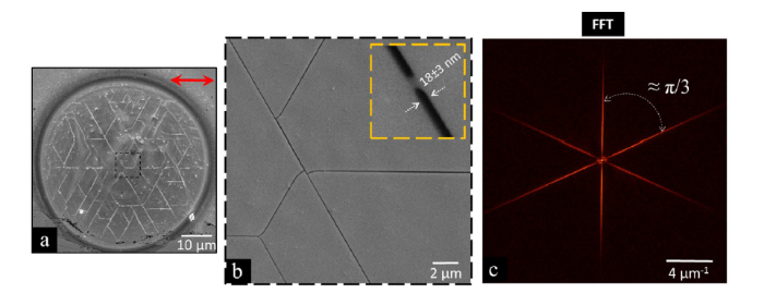
Fig. 2.
(a) SEM image of the CdZnTe surface after the irradiation with N = 20 pulses with energy E = 5 μJ (Fp = 0.64 J/cm2). The red arrow represents the laser polarization direction; (b) Zoomed view of the marked region in (a), clearly showing long cracks with nanometer width formed on the surface (see also inset); (c) 2D-FFT of the crater in (a), indicating that the cracks are formed along direction at angles multiples of π/3.
Analysis of several conditions suggest that the cracks are not orientated randomly but are instead disposed along particular angles and that the angle between couple of intersecting cracks is ≈π/3 or ≈2π/3. This is further verified by taking 2D-FFT of the spot with cracks, as shown in Fig. 2(c). This represents the distribution of the spatial frequencies in form of a star shaped intensity pattern with an angle of ≈π/3 between individual lobes.
The further evolution of the surface morphology of the CdZnTe sample after irradiation with larger number of laser pulses, at E = 5 μJ (Fp = 0.64 J/cm2), is reported in Fig. 3. At increasing N, the presence of surface cracks gets much clearer with formation of furrows around the cracks oriented in the same directions in the shallow circular area defined by the Gaussian profile of the laser beam. Fig. 3(a) and (b) reports SEM images of the surface after N = 30 laser pulses. It can be again noticed that all the cracks generated in the surface are always directed along three specific directions, indicated as I, II, and III in Fig. 3(b). Furthermore, as marked in the SEM image of Fig. 3(b), the angles formed between type I, II, and III cracks are mostly observed at around ≈π/3 or ≈2π/3, indicating that all cracks found in the crater are always found to be parallel to one of the sides of an equilateral tringle. A zoomed view in Fig. 3(b) also shows the formation of nano-holes arrays with a period of (698 ± 60) nm along the cracks direction at larger N. Fig. 3(c-f) displays the morphology of the crater for N = 50 laser pulses. Here the crater shows a more complex pattern mostly consisting of intersecting furrows identified as type I and II in the inner part of the spot. At the crossing of the deeper type I and II structures, rhombus shaped micro bumps form on the target surface, as marked in Fig. 3(d). However, in this condition surface structures oriented as type III are mostly found near the boundary of the crater, as shown in Fig. 3(f). Apart from that, randomly distributed surface defects in the form of nano-holes can be found all over the crater area. However, a number of nano-hole arrays with period of ≈800 nm are observed in the region irradiated by the less intense part of the laser beam, as shown in Fig. 3(e-f). More importantly, these arrays of nano-holes are typically found along the direction of type III cracks, which is also the direction perpendicular to the laser polarization. Therefore, the near-wavelength period and orientation of nano-holes seems to point to formation mechanisms similar to those typically involved in the classical subwavelength ripple formation. Fig. 3(g) shows the sample surface after irradiation with N = 100 laser pulses. At such pulse number, for E = 5 μJ, a deeper crater is formed and well-developed micro-columnar surface features appear over the central region corresponding to the most intense part of the beam. A zoomed view of the same region is shown in Fig. 3(h). This suggests that the micro-bumps seen at lower N in the Fig. 3(d) progressively evolve into columnar shaped structures as N increases reaching 100 laser pulses. A high-resolution image of the surface of the micro-columnar features is displayed in Fig. 3(i), whose morphology suggests that the columnar structures can be formed by aggregation of nanoparticles or nano-clusters and re-solidification processes. Moreover, in Fig. 3(g) one can also identify along the edges of the crater an extensive formation of groove-like structures oriented along the laser polarization along with arrays and randomly distributed nano-holes. Finally, it is worth to noticing that, the SEM images show only a very minimal trace of nanoparticles around the ablation spot in this experimental condition. For instance, the amount of nanoparticles is very much reduced in comparison to ablation of silicon [41,42], one of most studied material. This is likely due to the melting or re-ablation of the particles by the successive pulses due to the very low single pulse ablation threshold of the material.
Fig. 3.
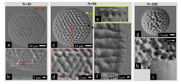
Fig. 3.
SEM images of CdZnTe after irradiation with a sequence of various number of pulses N, at E = 5 μJ (Fp = 0.64 J/cm2) and corresponding zoomed views: (a, b) N = 30; (c-f) N = 50; (g-i) N = 100. The red arrow in panel (a) indicates the laser polarization direction. In the zoomed view of panel (b) cracks directed along three different directions are indicated and termed as type I, II, and III. Panel (d) shows the central region of the spot displayed in panel (c) evidencing periodic bumps separated by cracks, while periodic arrays of subwavelength holes formed close to the spot edges are shown in panels (e, f). The zoomed view of panel (h) addresses the columnar features formed at the center of the spot for N = 100.
Before passing to the analysis of the effects of higher pulse energy and larger number of shots, we make an attempt to argue about the possible mechanisms leading to the formation of cracks. The particular alignment of the cracks suggests a connection of their formation mechanism with the structural properties of the sample material. The cracks likely form after melting and re-solidification of the irradiated material surface and their generation could result from different thermal coefficients of the sample components or structural defects already present in the original material. Structural imperfections in CdZnTe have been extensively investigated and dispersed Te inclusions are reported as one of the main bulk defects [34,43]. High grade CdZnTe is usually free from large-scale defects, such as grain boundaries, twins, and large Te or Cd inclusions (>50 μm), but it comes with abundance of small, uniformly distributed Te inclusions with a diameter in the range of ≈20 μm [43]. The trapping of Te-rich melts at the solid-liquid interface during the crystal growth in Te abundant conditions, typically used to optimize electrical characteristics, ultimately leads to formation of Te inclusions [35]. As metal matrix composite undergoes a temperature change, the residual stress due to the thermal expansion coefficients mismatch between inclusions and matrix causes a punching out of dislocations into the matrix, forming a dislocations rosette [44]. The detailed explanation of the formation of Te inclusions and related effects can be found elsewhere [15,43] and is out of the scope of this discussion. It has been shown that structural imperfections induced by Te inclusions are in the shape of a stellated octahedron, which is incorporated by two {111} Thompson’s tetrahedrons and is surrounded by dislocation-related defects [15]. This happens during the slow cooling process of ingot in the crystal growth process. During fs laser irradiation, the irradiated area undergoes fast melting followed by a sudden cooling, resulting in stress formation in the lattice due to the different thermal expansion coefficients of Te inclusion and matrix. This may result in formation of cracks in specific directions, similarly to the formation of dislocations rosette patterns surrounding Te inclusions on re-solidification of melt layer. This could be the reason why the cracks are formed only at particular directions, as shown in Fig. 2. In this case, there should be no direct correlation between the direction of the individual cracks and the laser polarization, and cracks orientation should be more related to alignment of Te inclusions in the material lattice and crystal cut. For instance, a study related to the effect of indentation on CdZnTe detector performances by Vicker’s hardness tester reveals the formation of similar cracks around the indentation points [45]. In such a case, it is clearly shown that the dislocations are propagated around the indentation center forming a rosette-like pattern that, consequently, degrades the spectroscopic properties of the CdZnTe detectors. In a similar way, fs laser pulse irradiation might result in the formation of dislocation defects in the surface layer, indicated by the cracks formation probably by the propagation of rosette. However, further investigations and surface characterizations are needed to fully clarify such an issue.
High pulse energy (fluence) and large number of pulses typically lead to the formation of a deep crater surrounded by a significant debris of nanoparticles resulting from the backward deposition of the ablated material around the crater due to the confining effect of the atmospheric air pressure [46]. Interestingly, in such a situation one can also observe the generation of well-ordered periodic surface structures in the sample surface region outside the main crater, where the local fluence is very much lower to that of peak fluence of the irradiating laser beam, as displayed for example in Fig. 4(a) and (b). In this case, the SEM images evidence the presence of ripples outside the deep crater formed with N = 500 and N = 1000, respectively, at E = 55 μJ (peak fluence Fp≈7.0 J/cm2). As shown in the insets of of Fig. 4(a) and (b), periodic LIPSS perpendicular to the laser polarization are formed over an annular area surrounding the deep crater (indicated by arrows pointing outside). For instance, at N = 1000 the ripples are found over a ring characterized by an average radial distance of ≈60 μm from the center of the crater spot and with a thickness of the annular disk of ≈20 μm. This region corresponds to extremely low values of the local laser pulse fluence (< 1 mJ/cm2). The spatial period of the surface ripples shown in Fig. 3(a) (N = 500) suggests the presence of both LSFL and HSFL over the same area (see Fig. 3(c) and (e)), whereas in the case of N = 1000 only HSFL cover the annular region (see Fig. 3(d) and (e)). Fig. 4(c) and (d) shows the 2D-FFT spectra of the SEM images of the ripples are shown in panels, respectively, while profiles taken along the dotted lines are displayed in Fig. 4(e). The 2D-FFT analysis supports the coexistence of both kind of ripples for N = 500 and the predominance of HSFL for N = 1000. From SEM images, at N = 500 the periods of LSFL and HSFL are ΛLF=(491 ± 35) nm and ΛHF=(204 ± 16) nm, respectively. For N = 1000, the spatial period of HSFL is ΛHF=(230 ± 29) nm. It is interesting to observe that the fluence values at which the ripples forms are below the threshold fluence for ablation expected from the incubation behavior discussed earlier, that are expected to be in the range 0.3-0.4 mJ/cm2 for 500 ≤ N ≤ 1000 laser pulses. This suggests that such structures are formed in a regime of irradiation below the ablation threshold and might likely involve a modification on the layer of nanoparticles deposited by previous pulses. This observation is similar to the generation of nanoparticles-based LIPSS reported earlier by Talbi et al. [47], who addressed the formation of linear subwavelength ripples perpendicular to the laser polarization through the progressive aggregation of randomly distributed nanoparticles during irradiation of mesoporous silicon with UV ps laser pulses at fluence below the ablation threshold and after many laser pulses. In that study, only LSFL were observed, while in our case also HSFL are formed suggesting that both type of LIPSS can be generated starting from nanoparticles arrays. Fig. 5 reports a sequence of SEM images of the LIPSS evolution with the pulse number N. The SEM image in Fig. 5(a), at N = 300, suggests the presence of HSFL rudiments even before the formation of well-developed LSFL. Then, at N = 500 (Fig. 5(b)) both type of LIPSS coexist. Finally, at increasing values of N the LSFL seem to be progressively demolished and eventually the surface is completely decorated by HSFL at N = 1000 (see Fig. 5(c)).
Fig. 4.

Fig. 4.
Low frequency and high frequency periodic surface structures formed on CdZnTe sample at an energy of E = 55 μJ (peak fluence Fp≈7.0 J/cm2) for high pulse number N, namely (a) N = 500 and (b) N = 1000. The corresponding FFT spectra are shown in panels (c, d), while panel (e) displays the profiles taken over the white dotted lines shown in panels (c, d). In panels (c-e) the term LF and HF indicate low and high spatial frequency, respectively.
Fig. 5.
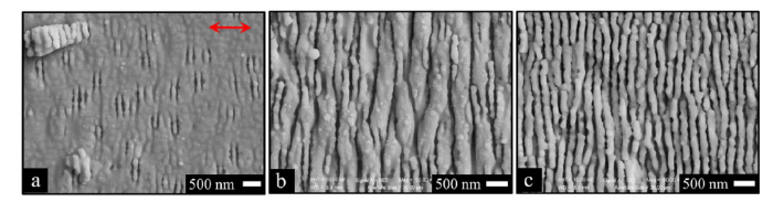
Fig. 5.
Sequence of SEM images displaying the evolution of the LIPSS formed on sample surface after irradiation with (a) N = 300, (b) N = 500 and (c) N = 1000 laser pulses at E = 55 μJ. The double headed arrow in panel (a) represents the direction of laser polarization.
Our experimental findings evidence various effects such as the generation of cracks and surface textures at low laser fluence as well as the formation of surface periodic ripples in the outskirts of the main crater at larger fluence. The fast laser melting and resolidification associated to fs laser ablation and processing can also induce structural and compositional changes [30]. All these effects might have potential interest for the fabrication of infrared and radiation detectors as well on CdZnTe-based detector performances, however these aspects are beyond the scope of this preliminary investigation and will deserve further experimental studies.
4. Conclusions
The direct band gap CdZnTe ternary semiconductor alloy is considered an ideal material for various applications (e.g. nuclear-radiation detectors, solar cells, electro-optical modulator, photoconductors, light emitting diode, etc). However, very few studies have been devoted to laser ablation and surface structuring of this compound. Here we have carried out an experimental study of laser ablation and surface structuring of CdZnTe by 800 nm, ≈35 fs laser pulses, in air.
One set of experiments, concerning irradiation of the sample with a fixed number of laser pulses, N, at various pulse energy, E, ascertained a clear incubation behavior of the threshold fluence to induce laser ablation and a single shot ablation threshold fluence of ≈14 mJ/cm2 and an incubation coefficient of ≈0.8.
A second set of experiments was carried out by irradiating the sample surface with a sequences of N laser shots (5≤ N ≤50) at low fluence (E≈5-10 μJ). These experiments show the interesting formation of a shallow crater presenting a number of well-defined cracks. The formation of the cracks has been tentatively associated to a different thermal expansion coefficient of Te inclusions and matrix during the heating and cooling processes associated to fs laser irradiation.
A final set of experiment were carried out at large number of pulses (N≈500, 1000) and with high pulse energies (E≈30-50 μJ), which result in the formation of a well-defined deep crater inside the material. Strikingly, the crater drilling is accompanied by the formation of laser-induced periodic surface structures (LIPSS) in an annular region corresponding to a low fluence region in the tail of the Gaussian beam out of the deep crater. Both LSFL and HSFL perpendicular to the laser polarization are observed and ascribed to a process of progressive aggregation of randomly distributed nanoparticles ensuing the laser ablation process at high pulse energy producing the deep crater. Our experimental findings evidence a variety of effects related to laser irradiation of CdZnTe with energetic fs pulses that can be of interest in laser processing, ablation and structuring of this material. LIPSS formation only at very high number of pulses indicates that even though the ablation threshold is much less than that of silicon the surface energy modulation required for the engraving of periodic features is achieved only at very high N. This further points towards the special condition required for surface wave excitation in CdZnTe, which is not found in the intense part of the beam and deserves further studies.
Reference
DOI
URL
PMID
[Cited within: 1]

We are investigating the feasibility of a high resolution positron emission tomography (PET) insert device based on the CdZnTe detector with 350 microm anode pixel pitch to be integrated into a conventional animal PET scanner to improve its image resolution. In this paper, we have used a simplified version of the multi pixel CdZnTe planar detector, 5 mm thick with 9 anode pixels only. This simplified 9 anode pixel structure makes it possible to carry out experiments without a complete application-specific integrated circuits readout system that is still under development. Special attention was paid to the double pixel (or charge sharing) detections. The following characteristics were obtained in experiment: energy resolution full-width-at-half-maximum (FWHM) is 7% for single pixel and 9% for double pixel photoelectric detections of 511 keV gammas; timing resolution (FWHM) from the anode signals is 30 ns for single pixel and 35 ns for double pixel detections (for photoelectric interactions only the corresponding values are 20 and 25 ns); position resolution is 350 microm in x,y-plane and approximately 0.4 mm in depth-of-interaction. The experimental measurements were accompanied by Monte Carlo (MC) simulations to find a limitation imposed by spatial charge distribution. Results from MC simulations suggest the limitation of the intrinsic spatial resolution of the CdZnTe detector for 511 keV photoelectric interactions is 170 microm. The interpixel interpolation cannot recover the resolution beyond the limit mentioned above for photoelectric interactions. However, it is possible to achieve higher spatial resolution using interpolation for Compton scattered events. Energy and timing resolution of the proposed 350 microm anode pixel pitch detector is no better than 0.6% FWHM at 511 keV, and 2 ns FWHM, respectively. These MC results should be used as a guide to understand the performance limits of the pixelated CdZnTe detector due to the underlying detection processes, with the understanding of the inherent limitations of MC methods.
DOI
URL
PMID
[Cited within: 1]
We investigate laser ablation of crystalline silicon induced by a femtosecond optical vortex beam, addressing how beam properties can be obtained by analyzing the ablation crater. The morphology of the surface structures formed in the annular crater surface allows direct visualization of the beam polarization, while analysis of the crater size provides beam spot parameters. We also determine the diverse threshold fluences for the formation of various complex microstructures generated within the annular laser spot on the silicon sample. Our analysis indicates an incubation behavior of the threshold fluence as a function of the number of laser pulses, independent of the optical vortex polarization, in weak focusing conditions.

 WeChat