


Effect of Fe Content on the Interfacial Reliability of SnAgCu/Fe-Ni Solder Joints
[Hao Zhang1 , Qing-Sheng Zhu1 , Zhi-Quan Liu1, *  , Li Zhang
2 , Hongyan Guo2 , Chi-Ming Lai2 ]
, Li Zhang|
|


Fe-Ni films with compositions of Fe-75Ni, Fe-50Ni, and Fe-30Ni were used as under bump metallization (UBM) to evaluate the interfacial reliability of SnAgCu/Fe-Ni solder joints through ball shear test, high temperature storage, and temperature cycling. The shear strengths for Fe-75Ni, Fe-50Ni, and Fe-30Ni solder joints after reflow were 42.57, 53.94 and 53.98 MPa, respectively, which were all satisfied the requirement of industrialization (>34.3 MPa). High temperature storage was conducted at 150, 175 and 200 °C. It was found that higher Fe content in Fe-Ni layer had the ability to inhibit the mutual diffusion at interface region below 150 °C, and the growth speed of intermetallic compound (IMC) decreased with increasing Fe concentration. When stored at 200 °C, the IMC thickness reached a limit for all three films after 4 days, and some cracks occurred at the interface between IMC and Fe-Ni layer. The activation energies for the growth of FeSn2 on Fe-30Ni, Fe-50Ni, and Fe-75Ni films were calculated as 246, 185, and 81 kJ/mol, respectively. Temperature cycling tests revealed that SnAgCu/Fe-50Ni solder joint had the lowest failure rate (less than 10%), and had the best interfacial reliability among three compositions.
Accompanying the fast development of lead-free soldering in microelectronic industry, traditional under bump metallization (UBM) materials such as copper and electroless nickel are consumed quite quickly due to the higher reflow temperature of lead-free solders than that of SnPb solders[ 1], [ 2], [ 3],[ 4]. On the other hand, solder joints are getting smaller due to the increased package density[ 5],[ 6]. Therefore, advanced high density packaging processes like chip scale packaging (CSP) face new challenges of interfacial reaction and reliability issues[ 7], [ 8],[ 9].
As reported, Fe-Ni alloy exhibits a much slower interfacial reaction rate than traditional UBMs using typical Pb-free solders[ 10], and the shear strength of SnAgCu solder joint could be slightly improved by replacing the Cu/Ni UBM with the Fe-Ni UBM[ 11]. Moreover, with adequate pre-treatment during soldering, the wettability of Fe-Ni UBM is also quite acceptable[ 12]. Thus Fe-Ni alloy is a good candidate for novel UBM materials. In this study, the interfacial reliability of SnAgCu/Fe-Ni solder joints was tested by high temperature storage, temperature cycling, and ball shear tests complying with the requirement of JEDEC standards.
Fe-Ni UBM films were deposited with a customized 8-inch (~20.3 cm) wafer electroplating system with detailed compositions of the plating bath as described elsewhere[ 13]. The wafer plating parameters were as follows: 1500 A/m2, 50 °C, 10 min, pH = 2.2. Iron content in the deposit was regulated by adding different amounts of Fe2+ to the plating bath, and three separate compositions of Fe-Ni UBM were prepared (Fe-75Ni, Fe-50Ni and Fe-30Ni) with thickness of about 1 μm. After plating, three pieces of wafer were subject to the following process: photoresist removal, Cu etching, solder ball plating, and solder reflow. Sn98.5Ag1Cu0.5 (SAC105) solder balls with 300 μm in diameter were reflowed at about 250 °C for 2 min. All samples reflowing were completed with practical production equipment under the same reflowing profile, which could ensure the exactly same soldering conditions.
The packaged wafer was separated into square pieces (10 mm × 10 mm) by precision wafer cutting and each piece had approximately 400 solder balls. High temperature storage (HTS) tests at 150, 175 and 200 °C were designed according to JEDEC-22A103D, considering the storage time and experiment cost as well as the accelerating effect during high temperature exposure. The temperature cycling (TC) condition listed in Table 1 was selected according to JEDEC-22A104D standard. Tested SAC105/Fe-Ni joints were sampled respectively after different days of storage test, and quantitative analysis on the destruction rate of joints was performed.
| Table 1. Temperature cycling text condition |
To observe the interfacial microstructure, the samples for scanning electron microscopy (SEM) observation were sealed in transparent epoxy resin, and were ground with silicon carbide papers of 400#, 1200#, 2000# in sequence. The samples were then polished by polishing solution with 0.05 μm diameter particle media until the SAC/Fe-Ni interface could be clearly seen by optical microscopy. Prior to SEM analysis, Nitric acid-95% alcohol solution was utilized to etch the SAC/Fe-Ni interface for nearly 5 s. Detailed interfacial microstructure of HTS samples was characterized by LEO Supra35 field-emission SEM with a resolution down to tens of nanometers. TC sample data was collected on a Quanta 600 SEM. Both electron microscopes were equipped with an energy dispersive X-ray spectroscopy (EDS) system for compositional analysis. The thickness of IMC layers was measured in a wide range using the image analyses software on SEM images as described before[ 14].
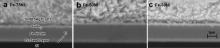
Fig. 1 exhibits interfacial microstructure of three kinds of as-reflowed SAC105/Fe-Ni joints in which Fig. 1(a) has been taken as an example to illustrate the layer microstructure. According to EDS analysis, a thin FeSn2 layer has formed between all three Fe-Ni UBM compositions and SAC105 solder balls after equivalent reflowing condition. The thickness of FeSn2 IMC on Fe-75Ni, Fe-50Ni, Fe-30Ni was measured as 0.342, 0.338 and 0.256 μm, respectively.
 | Fig. 1. Interfacial morphology of different Fe-Ni UBM barrier layers after reflow: (a) Fe-75Ni, (b) Fe-50Ni, (c) Fe-30Ni. |
Ball shear testing was conducted on as-reflowed solder joints with different Fe content, and the results are shown in Fig. 2. The test height was 25 μm from sample surface, and the shear speed was 100 μm/s. The average shear strength of solder joints with Fe-75Ni, Fe-50Ni, Fe-30Ni UBM layer is 42.57 ± 0.9, 53.94 ± 2.1, 53.98 ± 1.1 MPa, respectively, showing an increasing trend when Fe content is above 50%. It was reported that Fe-Ni plating with high-Fe component had poorer wettability than that of lower Fe content, which was seemingly corroborated by perceptible sealing-off rate of high-Fe CSP samples[ 15]. Generally speaking, poor wettability is directly related to inferior joint shear strength. However, in this work, high-Fe concentration samples had the higher shear strength, which should be related to the conditions of IMC layer. The thinner the IMC layer and the straighter the interface, the higher the shear strength of the solder joints[ 16], [ 17]. The SAC/Fe-30Ni interface possesses the thinnest IMC layer after reflowing, and its higher shear strength is consistent with this observation. Moreover, to characterize the wetting ability properly, average wetting angle but not the surface sealing-off rate is much accurate, which needs to be investigated further.
 | Fig. 2. Ball shear test result on as-reflowed SAC/Fe-Ni solder joints. |
HTS experiments were executed at 150, 175 and 200 °C on three kinds of SAC/Fe-Ni joints, to simulate continuous thermal load in practical usage and investigate the interfacial evolution during aging. Fig. 3 shows the typical interfacial microstructure of these samples stored at 150 °C over 27 days. Interfacial IMC of SAC/Fe-75Ni joints thickened significantly after 9 days aging due to the formation and growth of CuNiSn or (Cu,Ni)6Sn5 outside of FeSn2 layer. It must be pointed out that CuNiSn is not strictly proportional chemical formula and could be regarded as the immature state of (Cu,Ni)6Sn5[ 18]. The IMC and SAC105 interface is straight and free of interstate cracking and spalling as displayed in Fig. 3(d). A thickness limit for the growth of FeSn2 in Fe-75Ni/SAC interface was observed, which is due to the complete consumption of Fe during extended aging. For example, FeSn2 thickness increased from 1.6 μm in 9 days storage to 2.0 μm in 15 days storage. After that, no obvious increase of FeSn2 thickness was found even the aging time was extended up to 27 days, which could be illustrated in Fig. 3(d) and (g). However, SAC/Fe-50Ni and SAC/Fe-30Ni solder joints retain interfacial microstructure in which the thickness of FeSn2 layer is only 0.91 and 0.74 μm, respectively after 27 days (see Fig. 3(h) and (i)). Moreover, isolated granular-like CuNiSn compounds generated at the external side of FeSn2 layer, forming a discontinuous and irregular IMC layer. Although the outer CuNiSn IMC layer shows an inclination to spalling with aging time, entire-layer spalling could not be seen as shown in Fig. 3(h) and (i).
 | Fig. 3. Interfacial morphology of different Fe-Ni solder joints after 1, 9 and 27 days′ aging in 150 °C: (a)-(c) 1 day, (d)-(f) 9 days, (g)-(i) 27 days. |
When stored at 200 °C, the interfacial IMC in all three kinds of samples displayed a rapid thickening in relatively short period. For instance, after storage for 1 day part of the interfacial SAC/Fe-75Ni IMC joint spalls as an entire layer and drifts to the internal part of solder ball as shown in Fig. 4(a). The thickness of the FeSn2 layer in SAC/Fe-75Ni joint reaches 2 μm after 1 day, and the Cu seed layer cannot be clearly distinguished in the enlarged image of Fig. 4(d), which demonstrates that atoms at 200 °C have the ability of full mutual diffusion in a short time, thereby causing a composition unification trend in each layer. Fig. 4(e) shows the detailed morphology of SAC/Fe-75Ni joints after 4 days storage at 200 °C. The former FeSn2 layer has grown into 2-3 μm thick, and a transverse crack forms between it and substrate with zigzag interface morphology. Continuous scallop-like (Cu,Ni)6Sn5 layers form on the FeSn2 layer, and interfacial voids can be observed between those two layers. The drifting of outer IMC seems in progress, and the composition of bottom Cu seed layer has already transformed into a Sn-rich complex composition. This implies that the normal interfacial structure of SAC/Fe-75Ni has been seriously destructed after aging for 4 days at 200 °C. After 15 days storage at 200 °C, spalling of granular or lamellar IMC with 10 μm diameter was observed in solder balls near the (Cu,Ni)6Sn5/SAC interface as shown in Fig. 4(b). After 27 days, interfacial IMC layer has completely spalled and drifted to internal parts of solder ball (Fig. 4(c)). The same situation occurred at SAC/Fe-50Ni and SAC/Fe-30Ni interface, indicating that the variable Fe composition had no effect on the interfacial reaction in SAC105/Fe-Ni solder joints at a temperature as high as 200 °C.
 | Fig. 4. Interfacial morphology of Fe-75Ni solder joint after different days′ aging in 200 °C: (a) 1 day, (b) 15 days, (c) 27 days, (d) 1 day (microscopic morphology), (e) 4 days (microscopic morphology). |
In solid state reaction, the relationship between thickness of IMC and aging time could be summarized as the formula below[ 19]:
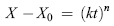 | (1) |
where X0 and X are the initial and ultimate thickness of IMC layer, respectively. The value of time index n is determined by the detailed mechanism of interfacial reaction. When n is equal to 1 or 1/2, the growth of IMC should be dominated by surface reaction mechanism or bulk diffusion mechanism, respectively.
Fig. 5 shows the growth behavior of FeSn2 compound stored at different temperatures. As it can be seen from Fig. 5(a), the relationship between the IMC thickness on three kinds of Fe-Ni UBM barrier layer and the square root of aging time is approximately linear under 150 °C, which demonstrates that in all of the interfacial reaction systems diffusion is the reaction rate controlling step. The thickness data of FeSn2 layer in SAC/Fe-75Ni interface are only covered before 15 days in the data-fitting of Fig. 5(a), because after that the thickness of FeSn2 reaches its growth limit. The same situation occurs in SAC/Fe-75Ni interface after aging at 175 °C for 9 days as shown in Fig. 5(b). The growth speed of FeSn2 layer in SAC/Fe-75Ni interface is obviously higher than that in other two kinds of SAC/Fe-Ni interface. In addition, thickening speed of FeSn2 layer decreases with growing Fe composition, which agrees well with the IMC growth kinetics in Fe-Ni/Sn-58Bi system[ 20].
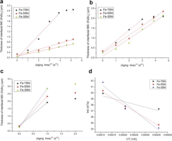 | Fig. 5. Relationship between the thickness of IMC and time in SnAgCu/Fe-Ni systems under high temperature storage: (a) 150 °C, (b) 175 °C, (c) 200 °C, (d) relationship between 1/ T and ln k. |
For the growth behavior of FeSn2 at 200 °C, after 1 day aging severe growth of FeSn2 layer appears at all the three SAC/Fe-Ni joints, and after 4 days storage the three FeSn2 layers have totally reached their growth limit. The thickness limit of FeSn2 layer displays an approximately linear relationship with Fe composition in plating, which is shown in Fig. 5(c). The higher the Fe composition, the thicker the growth limit of FeSn2 layer. The composition of Fe in plating would finally determine the ultimate thickness of FeSn2 layer for the reason that resource of Fe element was exclusively Fe-Ni plating and Fe had no tendency of diffusion to the internal part of solder. Therefore, Fe element would finally contribute to the growth of FeSn2 layer.
Growth kinetics of IMCs under specified temperature is usually defined by formula below[ 10]:
 | (2) |
where k and Q are growth rate constant and activation energy of IMC, respectively, R and T are ideal gas constant and absolute temperature, respectively. Activation energies for the growth of FeSn2 in SAC/Fe-75Ni, SAC/Fe-50Ni, SAC/Fe-30Ni systems can be calculated from the data in Fig. 5(d), which are 81, 185, and 246 kJ/mol, respectively. Comparing these data with those in Sn-58Bi/Ni-56Fe system (FeSn2, 154 kJ/mol)[ 20], Sn-58Bi/Ni system (N3Sn4, 90 kJ/mol)[ 21], Sn-9Zn/Ni-58Fe system (Fe-Zn phase, 42 kJ/mol)[ 22] and Sn-3.5Ag/Ni system (Ni3Sn4, 91 kJ/mol)[ 23], it can be found that Fe-Sn phase and Ni-Sn phase usually have a relatively higher activation energy for the growth of IMCs.
SEM examination was used to quantitatively evaluate the interfacial cracking rate, and the morphology of two typical cracks is shown in Fig. 6. Cracks initiate and propagate at the Cu(Ti)/Si interface in most samples, which will eventually result in transverse fracture along the interface as shown in Fig. 6(a) and (c). Moreover, significant crescent shaped cracking was observed in Si substrate beneath the solder ball as seen in Fig. 6(b) and (d).
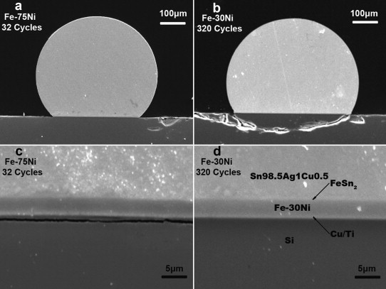 | Fig. 6. SEM images of interfacial cracks caused by temperature cycling: (a) and (c) Fe-75Ni solder joint after 32 cycles, (b) and (d) Fe-30Ni solder joint after 320 cycles. |
The interfacial damage data are summarized in Table 2. The numbers before “/” represent the amount of balls with cracks along the interface, while numbers after “/” represent the total amounts of samples. Numbers in “()” represent amounts of balls with Si substrate cracks. It can be seen from Table 2 that SAC/Fe-75Ni joints exhibit a relatively higher failure rate after 32 cycles, and the incidence of joint destruction has reached 68% after 640 cycles. SAC/Fe-30Ni joints show a relatively high incidence of cracks in the Si substrate, consistent with interfacial thermal stress release. The failure rate of SAC/Fe-50Ni solder joint is the lowest, with a degradation rate less than 10% including both types of cracks, which shows the best interfacial reliability among three compositions.
| Table 2. Statistical analysis of interfacial crack after different cycles of TC test |
(1)After reflow, the SAC/Fe-75Ni solder joint had the thickest FeSn2 IMC layer on top of which there existed granular-like CuNiSn IMC, while SAC/Fe-30Ni had the thinnest sole FeSn2 layer. The shear strengths for Fe-75Ni, Fe-50Ni, and Fe-30Ni reflowed solder joints were 42.57, 53.94, 53.98 MPa, respectively, which satisfied the requirement of industrialization (>34.3 MPa).
(2)During high temperature storage at 150 °C, Fe-75Ni films (1 μm thick) exhibited an obvious IMC growth (up to 10 μm thick) after 9 days' aging, while Fe-50Ni and Fe-30Ni films could endure 27 days' aging with less consumption of the Fe-Ni layer. When stored at 200 °C, Fe-75Ni, Fe-50Ni and Fe-30Ni films reached the growth limit of FeSn2 within 4 days, which was 2.2, 2.6, and 3.3 μm, respectively. Activation energies for the growth of FeSn2 in SAC105/Fe-75Ni, SAC105/Fe-50Ni, SAC105/Fe-30Ni systems, were measured as 81, 185, and 246 kJ/mol, respectively.
(3)During temperature cycling, a significant occurrence of cracks was observed at the Ti/Si interface of SnAgCu/Fe-75Ni solder joints with a destructive rate of 20%-40%. Fe-30Ni solder joint exhibited a small amount of substrate cracks under the Ti/Si interface, while less cracks were observed on the Ti/Si interface. The Fe-50Ni solder joint had relatively better reliability than other two compositions, and the destructive rate was less than 10%.
Acknowledgments
We gratefully acknowledge the financial support from the Hundred Talents Program of the Chinese Academy of Sciences, the National Natural Science Foundation of China (Grant No. 51101161), the National Basic Research Program of China (Grant No. 2010CB631006), and the Major National Science and Technology Program of China (Grant No. 2011ZX02602).
| 1. |
|
| 2. |
|
| 3. |
|
| 4. |
|
| 5. |
|
| 6. |
|
| 7. |
|
| 8. |
|
| 9. |
|
| 10. |
|
| 11. |
|
| 12. |
|
| 13. |
|
| 14. |
|
| 15. |
|
| 16. |
|
| 17. |
|
| 18. |
|
| 19. |
|
| 20. |
|
| 21. |
|
| 22. |
|
| 23. |
|