

1. Introduction
In response to the increasing demand for CO2-free renewable energy with short energy payback time, organic solar cells (OSCs) have been intensively studied. These solar cells possess merits such as large area demonstration, low-cost fabrication, and compatibility with flexible substrates. Moreover, through continuous studies on the OSCs, power conversion efficiencies over 13% (as a single solar cell) have been achieved [1]. Thereby, the OSCs have emerged as strong candidates to lead the next generation renewable energy industry. The elevation of photovoltaic performance has involved not only introducing wide-wavelength range absorbers but also designing device architecture. One avenue for improving the device architecture is to add a charge transport layer with an embedded nanostructure that penetrates the active layer to collect charges more effectively. Such three-dimensional nanostructures can increase the surface area and function as scaffolds of transport pathways, increasing the charge extraction probability.
Numerous studies regarding an effective nanostructured charge transport layer inside the active layer have been conducted using vertically aligned nanorods (NRs) of materials such as TiO2 [[2], [3], [4], [5]], ZnO [[6], [7], [8], [9], [10], [11]], SnO2 [12,13], and Nb2O5 [14,15]. Crystalline NRs that are buried in the active layer are able to obtain dissociated electrons. Among them, ZnO has the superior electrical conductivity and transparency suitable for an electron transport. Based on its preferred properties, nanostructured ZnO has been widely utilized as an effective ETL for the OSCs. Diverse structures, such as ZnO NRs [[16], [17], [18], [19]], ZnO nanoforest [20], and others. [21,22], have been reported. In particular, Dongqin Bi et al. used the ZnO NRs with a controlled length from 400 nm to 1200 nm as the ETL [23], which sensitively affected device characteristics. In addition, Park et al. reported the influence of the ZnO NR fabrication method on the performance of solar cells, revealing the importance of a seed layer [24].
Based on former studies, the ZnO NRs have shown incomparable merits when used as the charge selective layer, which increases the electron diffusion length. The highly oriented structures amplify carrier mobility and suppress electron-hole recombination [25,26]. Nevertheless, conventionally fabricated ZnO NRs used in dye-sensitized solar cells (DSSCs) and perovskite solar cells are not as suitable for OSCs. This incompatibility might be ascribed to difficulties with surface defects [27] or a thin active layer. Generally, the thickness of the active layer in the OSCs is limited to hundreds of nanometers due to the short exciton diffusion length [28]. Therefore, the conventional specification of ZnO NRs, which is used in the DSSCs (˜10 μm) and perovskite solar cells (˜1 μm), cannot be used in the OSCs, because the ZnO NRs that exceed the active layer thickness induce a non-uniform morphology and a shunt path inside the OSCs. Likewise, an adequate length of the ZnO NRs is one of the most important variables determining photovoltaic performance. Their optical, physical and electrical characteristics individually influence the solar power conversion of photovoltaic cells.
In this work, we introduced a facile method to control the germinant step growth of ZnO NRs. We controlled the length of the NRs by varying the growth time in the precursor solution; at certain times, the reaction was aborted and rapidly chilled to provide an elaborate control. It is found that longitudinal increment of ZnO NRs results from the oriented growth of ZnO crystal after the seed swell by 85 nm. Based on this method, the OSCs adopting various lengths of ZnO NRs were fabricated to study the effect of ZnO NRs in an optoelectronic device. The physical dimensions and optical characteristics of ZnO crystalline structures which determine photovoltaic performance were enumerated. These multilateral factors provide the optimal structure of ZnO NRs in the OSCs, which show a significant increment of power conversion efficiency (PCE).
2. Experimental
2.1. ZnO seed and precursor solution preparation
The preparation of the seed solution was described in a former article [29]. Briefly, zinc acetate dehydrate [Zn(CH3COO)2·2H2O] (2.2 g) was dissolved in isopropanol (IPA) (50 mL). The solution was stirred for 20 min at 60 °C. Monoethanolamine (MEA) (0.6 mL) was dropwise added to make sure the complete dissolution. After the milky solution became transparent, it was maintained at 60 °C for 2 h. Precursor solution for vertical growth of the seed layer was prepared as follows: Zinc nitrate hexahydrate [Zn(NO3)2·6H2O] (3.72 g) was dissolved in deionized (DI) water (500 mL), hexamethylenetetramine (HMTA) was added at the same molar concentration as Zn(NO3)2, and 2 g of polyethylenimine (ethylene diamine branched, average molecular weight approximately 800) was added. The mixed solution was stirred for 20 min.
2.2. ZnO NR formation
First, indium tin oxide (ITO) substrate was cleaned using ultrasonication with acetone, IPA, and deionized (DI) water. Subsequently, the seed solution was spin-coated on ITO glass at 3000 rpm for 20 s. The deposited seed layer was dried on a hot plate at 150 °C for 10 min. To obtain a seed layer of sufficient thickness, the process was repeatedly performed following annealing at 500 °C for 2 h. The prepared seed layer was soaked in the precursor solution for growth and heated at 90 °C for various controlled times. After removal from the solution, the samples were repeatedly rinsed with DI water to eliminate any salt remaining on the film. Last, the ZnO NR film was annealed at 500 °C using a hotplate for 2 h.
2.3. Device fabrication
The polymer blend was prepared by dissolving 1:1.5 by a weight ratio of poly[(2,5-bis(2-hexyldecyloxy)phenylene)-alt-(5,6-difluoro-4,7-di(thiophen-2-yl)benzo[c]- [1,2,5]thiadiazole)] (PPDT2FBT) [6,6]:-phenyl-C71-butyric acid methyl ester (PC70BM) into a solvent mixture composed of chlorobenzene (CB) and diphenyl ether
(DPE) (98:2 by vol%). This yielded total concentrations of 30 mg mL-1 and 45 mg mL-1 for active layer thicknesses of 170 nm and 290 nm, respectively. The active layer was deposited on top of a ZnO NR-based film via spin-coating of the polymer blend at 1000 rpm for 60 s. Then, the active layer was annealed at 130 °C for 10 min in a glove box filled with Ar. Last, MoO3 (10 nm) and Al (100 nm) were thermally deposited.
2.4. Characterization
The current density (J-V) characteristics were measured using a source measurement unit (Tektronix, Keithley 237) with an AM 1.5 G solar simulator (Newport, 91160A). The transmittance was recorded using an ultraviolet/visible (UV/Vis) spectrophotometer (Beckman Coulter, US/DU 70 Series). The charge extraction property was characterized using an IPCE measurement system (Newport, QEPVSI-B). Cross-sectional images were obtained using field emission-scanning electron microscopy (FE-SEM) (Hitachi High-Technologies Europe GmbH, Hitachi S-4800) and transmission electron microscopy (TEM) (JEOL Ltd, JEM-2100 F). The crystallinity was measured using X-ray diffraction (XRD) (BRUKER MILLER Co., D8-Advance).
3. Results and discussion
The ZnO NR length can be controlled by the reaction time in the precursor solution during growth. Although more than 8 h are usually required to fabricate micrometer-long ZnO NRs, shorter lengths can be obtained by aborting the heating step and cooling down in an earlier stage. Fig. 1(a-e) show cross-sectional SEM images of ZnO NRs with different lengths controlled by the growth time, and a top-view image at 100 min of growth time is shown in Fig. 1(f). To characterize the length distribution of the ZnO NRs as a function of growth time, the temperature of the precursor solution and the average lengths of the NRs in Fig. 1 are plotted in Fig. 2(a). In a conventional convection oven, the temperature of the precursor solution was gradually increased until to 90 °C. After 60 min of growth, the salutation was saturated at the temperature of 90 °C, and the ZnO NRs start to grow. The average length and standard deviation of the NRs were calculated by compiling statistics on 30 randomly selected samples at three different locations. The average length increased from 45 nm at 60 min to 265 nm at 100 min with a relatively linear increment of 5.5 nm min-1. With an increase in the average length, the standard deviation also increased from 5 nm to 25 nm, with respect to the growth time. This is ascribed to the non-identical standing angle of each ZnO NR from the substrate plane.
Fig. 1.

Fig. 1.
Cross-sectional scanning electron microscopy (SEM) images of ZnO nanorods (NRs) after (a) 60 min, (b) 70 min, (c) 80 min, (d) 90 min, and (e) 100 min growth time and (f) a top-view image of ZnO NRs after 100 min growth time.
Fig. 2.
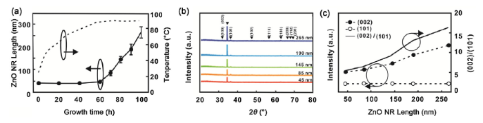
Fig. 2.
(a) Length profile of the ZnO nanorods (NRs), temperature of precursor solution as a function of growth time and (b) X-ray diffraction (XRD) patterns of the ZnO NRs with respect to growth time (black arrow: ZnO diffraction standards: JCPDS 36-1451) and (c) ratio of (002) peak to (101) peak.
The growth process of the ZnO NRs consists of the five chemical reactions listed above [30]. While Zn2+ ions are supplied by zinc nitrate salt (Eq. (4)), HMTA forms a weak base in water solution, which provides OH- (Eq. (1)-(3)). Finally, ZnO is synthesized by the dehydration reaction of Zn(OH)2 (Eq. (5)). Although the synthesis rate of each step is generally adjusted under the control of the ion concentration, those concentrations are scarcely changed over a relatively short reaction time. Therefore, the ZnO NRs show a relatively constant initial growth rate that ensures an easy control. This also makes them an appropriate candidate for use in the ETL of OSCs.
To characterize the crystallinity, XRD patterns were analyzed as a function of growth time (Fig. 2(b)). All the XRD patterns of the samples were indexed with that of the hexagonal wurtzite structure of ZnO. In comparison to several peaks of the diffraction standards (JCPDS 36-1451), the ZnO NRs only showed peaks corresponding to the (002), (101), (102), and (103) planes, whereas the (102) and (103) diffraction peaks were almost insignificant. The intensities of the (002) and (101) peaks of the XRD patterns are listed in Table 1. By increasing the length of ZnO NRs after 60 min of growth time, the XRD pattern also showed an increase in intensity. Among all peaks shown in the pattern, the (002) peak stood out as increasing more. Fig. 2(c) shows a comparison of the (002) peak and (101) peak of the XRD pattern. While the (002) orientation kept increasing during the growth of the ZnO NRs, there was no increase in the (101) orientation. The ratio of (002) to (101) was 5.55 at 45 nm NR length and 60 min of growth time. However, the ratio at 265 nm NR length and 100 min of growth time increased to 16.37, which agrees with anisotropy in the lattice orientation for z-axis growth of ZnO NRs observed in SEM images (Fig. 1).
Table 1 X-ray diffraction (XRD) peak ratio of ZnO nanorods (NRs) with respect to growth time.
| Peak | Length | ||||
|---|---|---|---|---|---|
| 45 nm | 85 nm | 145 nm | 190 nm | 265 nm | |
| (002) | 583 | 683 | 925 | 1278 | 1670 |
| (101) | 105 | 103 | 99 | 97 | 102 |
| (002)(101) | 5.55 | 6.63 | 9.34 | 13.17 | 16.37 |
The effect on light absorption by the ZnO NR length was studied through UV-vis absorption spectroscopy. Along with the length profile, the absorbance of the ZnO NR film with respect to the average length was measured (Fig. 3(a)). While the absorbance spectra in the visible region were almost negligible regardless of the NR length, the absorbance in the UV region at wavelengths < 380 nm started to drastically increase, and this wavelength region was constant regardless of the length of ZnO NRs. While the optical bandgap is invariable, its amplitude is increased by the NR length. The absorption by the charge transporting layer can affect the reach of light into the active layer in the full device. The bilayer sample is fabricated by depositing PPDT2FBT:PC70BM bulk heterojunction layer onto ZnO NRs of the same lengths in Fig. 3(a). Fig. 3(b) shows absorption spectra of a fabricated bilayer and of each layer. Absorbance in the visible range of wavelength which does not overlap those of the ZnO NRs, was consistent with that of an active layer without ZnO NRs. This indicates that ZnO NRs arrayed beneath the active layer have no effect on the structure formation of the bulk heterojunction. On the other hand, the absorbance of the bilayer increased at wavelengths < 380 nm owing to the absorption by the ZnO NRs. The increase in absorbance of the bilayer alludes to decrease in absorption by the PPDT2FBT individual active layer, because it means photons can be absorbed not by the active layer but by ZnO NRs in the light path of the medium of the bilayer. Further analyses to investigate the effect of this phenomenon will be explained in the following paragraph about the IPCE results.
Fig. 3.
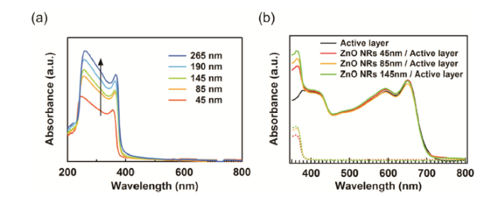
Fig. 3.
UV/Vis absorption spectra of (a) ZnO nanorods (NRs) with respect to length variation and (b) PPDT2FBT:PC70BM layer deposited on ZnO NR arrays of various length (line), ZnO NRs arrays without PPDT2FBT:PC70BM deposition (dotted line).
Inverted OSC structures with ZnO NRs as ETL were fabricated (Fig. 4(a)). The germinant growth of the ZnO NRs inside the OSC was verified through a cross-sectional TEM image (Fig. 4(b)). The measured thickness of the seed layer was ˜40 nm. Above the seed layer, the ZnO NRs were grown with randomly distributed lengths in the range of 100-200 nm. The ZnO NR length and active layer thickness were well matched without formation of a shunt path between the ZnO NR and MoO3/Al anode contact. To obtain a further insight into the correlation between the active layer thickness and the ZnO NR length, a photoactive layer of PPDT2FBT:PC70BM was adopted. It has been reported the high PCE (> 8%-9 %) is shown even with a thick active layer on the order of ˜300 nm [31]. PPDT2FBT exhibits broad absorption in the range of 350-750 nm and the thickness tolerance is closely related to its strong face-on crystalline blend morphology, which facilitates charge transport (e and h mobilities of ˜10-3 cm2 Vs-1) in the vertical direction. For an exhaustive comparison, the OSCs with two different active layer thicknesses (170 nm and 290 nm), and several ZnO NR growth times were fabricated and their results were compared (Table 2).
Fig. 4.
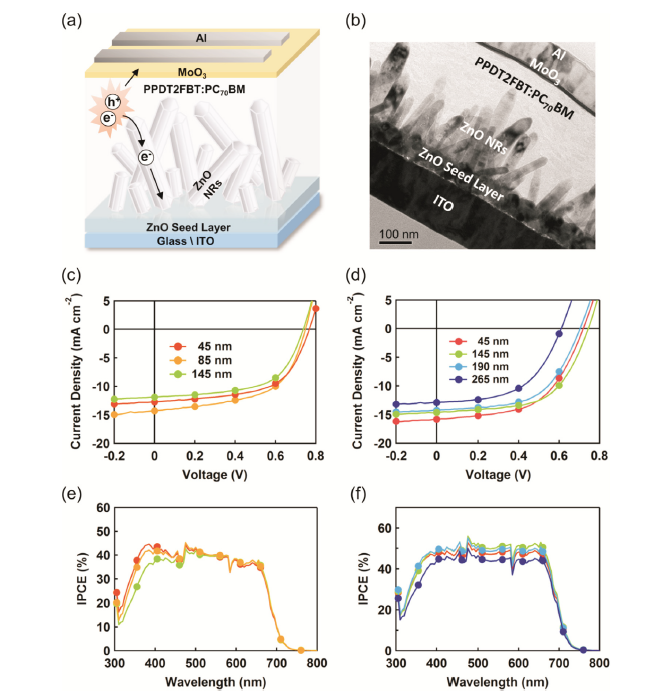
Fig. 4.
(a) Schematic illustration, (b) cross-sectional transmission electron microscopy (TEM) images of ZnO nanorods (NRs) organic solar cells (OSCs), current-voltage (J-V) characteristics and incident photon-to-current conversion efficiency (IPCE) of devices with (c, e) 170-nm- and (d, f) 290-nm-thick active layers, respectively.
Table 2 Performance parametersa of organic solar cells (OSCs) with respect to the active layer thickness and ZnO nanorod (NR) length.
| Active layer thickness | ZnO NRs Length | JSC (mA cm-2) | VOC (V) | FF | PCE (%) |
|---|---|---|---|---|---|
| 170 nm | 45 nm | 13.3 ± 0.65 | 0.75 ± 0.02 | 0.57 ± 0.02 | 5.62 ± 0.13 |
| 85 nm | 13.8 ± 0.85 | 0.75 ± 0.02 | 0.57 ± 0.03 | 5.91 ± 0.19 | |
| 145 nm | 12.5 ± 1.02 | 0.71 ± 0.04 | 0.58 ± 0.02 | 5.12 ± 0.09 | |
| 290 nm | 45 nm | 15.9 ± 0.17 | 0.71 ± 0.01 | 0.54 ± 0.01 | 6.10 ± 0.13 |
| 145 nm | 14.5 ± 0.46 | 0.73 ± 0.02 | 0.58 ± 0.01 | 6.20 ± 0.17 | |
| 190 nm | 14.4 ± 0.29 | 0.70 ± 0.01 | 0.56 ± 0.01 | 5.65 ± 0.01 | |
| 265 nm | 12.9 ± 0.21 | 0.58 ± 0.03 | 0.52 ± 0.01 | 3.89 ± 0.31 |
a Values were averaged for the three devices.
In a device with an active layer thickness of 170 nm (Fig. 4(c) and Table 2), the performance of the OSC increased from PCE = 4.93% (with a short-circuit current density (JSC) of 11.85 mA cm-2, open-circuit voltage (VOC) of 0.74 V and fill factor (FF) of 0.56) without NRs to PCE = 5.91% (JSC =13.86 mA cm-2, VOC = 0.75 V, FF = 0.57), as the length of the ZnO NRs grew to 85 nm. While VOC and FF maintained similar values with increases in the length of the NRs, the JSC showed a significant increase of 17%, which led to a PCE enhancement of 20%. This increase in performance is attributed to improved charge extraction by the ZnO NRs inside the active layer. However, as the ZnO NR length exceeded 145 nm, the OSC performance declined from PCE = 5.91% to 5.12% (JSC =12.56 mA cm-2, VOC = 0.71 V, FF = 0.58). This decrease in performance is due to two major factors: instrusion of some long ZnO NRs into the active layer and excess UV absorption by the ZnO NRs (Fig. 3(a)). This led to a decrease in light absorption in the active layer. Fig. 2(a) shows the variation of the ZnO NR length. The longer ones among them could intrude into the active layer. This is undesirable due to the possibility of shunt path formation between the ZnO NRs and MoO3/Al interface, which is in accordance with former articles that report the effect of a shunt path on the performance of solar cells [32]. In Fig. 4(c) and (e), the IPCE results show correlation between the length of ZnO NRs and the spectral power conversion efficiency. As the ZnO NR growth length increased from 45 nm to 145 nm in an active layer 170 nm thick, the IPCE started to drastically drop in the UV region, whereas the IPCE was maintained in the visible region. The drop of the IPCE in the UV region can be explained by UV absorption by the ZnO NRs. Absorbance by the ZnO NRs and its bilayer with active layer was already discussed earlier in Fig. 3 that the light absorption by the ZnO NRs was only at the UV region. When light illuminates a solar cell device, the UV light is blocked by the ZnO NRs and fewer photons reach the active layer.
The performance characteristics exhibit a similar trend for devices with an active layer thickness of 290 nm in terms of the PCE (Fig. 4(d) and (e)). Although there is a similar trend for the overall PCE, it shows a maximum peak in the middle (80 min for this case). The PCE of 6.20 at the maximum peak is higher than that with a 170 nm nanorod array because of the increased absorption by the thick active layer. By lengthening the nanorods from 145 nm of the maximum PCE, the photovoltaic factors drop drastically and result in the PCE decrement. With the 170 nm active layer, the decline of the spectral power conversion efficiency in the UV region was greater than the drop in the visible region. This drop in the J-V characteristics results from two previously discussed factors: development of shunt paths and increase in the UV absorption due to excess growth of the ZnO NRs.
The correlation between the ZnO NR growth time and PCE of OSCs with respect to the active layer thickness is plotted in Fig. 5. In both cases, the PCE shows an increase in performance up to an optimized point where it rapidly decreases afterwards, due to excess UV absorption and shunt path formation between the ZnO NR and MoO3/Al anode. Note that the performance of the OSCs demonstrated in this study requires further improvement to compare with high-performance OSCs [31]. Nevertheless, we conducted an in-depth study regarding the characteristics of ZnO NRs and successfully applied them to the OSCs, which are revealed to be promising candidates for using as ETLs. In this study, we propose a novel and effective method to synthesize and grow ZnO NRs with an easy control of their length, based on their growth time. Furthermore, the correlations between the ZnO NR length and active layer thickness were studied in detail, which revealed the importance of an optimized nanostructured ETL. This study provides useful insights for the development of high-performance OSCs with ZnO NRs as effective ETLs.
Fig. 5.

Fig. 5.
Power conversion efficiency (PCE) variations of organic solar cells (OSCs) depending on the active layer thickness and ZnO nanorod (NR) length.
4. Conclusion
We demonstrated a facile method for fabricating the ZnO NRs that ranged from 50 nm to 300 nm in length, and the length depends on the precursor reaction time. In-depth analyses including SEM, TEM, XRD, and absorbance measurements were conducted to characterize the film properties. The fabricated ZnO NRs of various lengths were used as charge selective layers in organic solar cells. There were three major factors that determined the performance of these organic solar cells. First, the three-dimensional morphology provided by the increased interfacial area of the ZnO NRs helped to improve charge extraction. Second, ZnO NRs longer than the thickness of the active layer aggravated the overall performance by forming shunt paths. Last, the blocking of UV light by the ZnO NRs induced spectral change of the light that reached the active layer. For these reasons, there is an optimal length of ZnO NRs to maximize solar cell performance, whose length differed according to the thickness of the active layer. Consequently, an OSC with PCE = 6.20% was successfully demonstrated with an ETL based on the ZnO NRs. This work provides new insights into, and adds to, the existing knowledge regarding the development of high-performance OSCs.
Author contribution
Kunsik An and Jaehoon Kim equally contributed to this work. Changhee Lee, Han Young Woo and Kunsik An organized the overall content of this research. Kunsik An synthesized ZnO nanorods and Jaehoon Kim fabricated the photovoltaic cells. Kunsik An, Jaehoon Kim, Seunghyun Rhee and Hyeok Kim characterized the device as well as its individual thin films. All authors reviewed and contributed to the final version of the manuscript.
Acknowledgements
This study was conducted with support from the Korea Institute of Industrial Technology as Research Source Technique Project (KITECH, EO-190008)
Reference
DOI
URL
PMID
[Cited within: 2]

A new polymer donor (PBDB-T-SF) and a new small molecule acceptor (IT-4F) for fullerene-free organic solar cells (OSCs) were designed and synthesized. The influences of fluorination on the absorption spectra, molecular energy levels, and charge mobilities of the donor and acceptor were systematically studied. The PBDB-T-SF:IT-4F-based OSC device showed a record high efficiency of 13.1%, and an efficiency of over 12% can be obtained with a thickness of 100-200 nm, suggesting the promise of fullerene-free OSCs in practical applications.
DOI
URL
PMID
[Cited within: 2]

Dye-sensitized solar cells (DSSCs) made from oriented, one-dimensional semiconductor nanostructures such as nanorods, nanowires, and nanotubes are receiving attention because direct connection of the point of photogeneration with the collection electrode using such structures may improve the cell performance. Specifically, oriented single-crystalline TiO(2) nanorods or nanowires on a transparent conductive substrate would be most desirable, but achieving these structures has been limited by the availability of synthetic techniques. In this study, a facile, hydrothermal method was developed for the first time to grow oriented, single-crystalline rutile TiO(2) nanorod films on transparent conductive fluorine-doped tin oxide (FTO) substrates. The diameter, length, and density of the nanorods could be varied by changing the growth parameters, such as growth time, growth temperature, initial reactant concentration, acidity, and additives. The epitaxial relation between the FTO substrate and rutile TiO(2) with a small lattice mismatch plays a key role in driving the nucleation and growth of the rutile TiO(2) nanorods on FTO. With TiCl(4)-treatment, a light-to-electricity conversion efficiency of 3% could be achieved by using 4 mum-long TiO(2) nanorod films as the photoanode in a DSSC.
DOI
URL
PMID
[Cited within: 1]
Highly crystalline TiO2 nanorods with lengths of 100-300 nm and diameters of 20-30 nm have been synthesized by a hydrothermal process in a cetyltrimethylammonium bromide surfactant solution. The microstructure measured by X-ray diffraction and high-resolution transmission electron microscopy was a pure highly crystalline anatase phase with a long nanorod shape. The addition of a triblock copolymer poly(ethylene oxide)100-poly(propylene oxide) 65-poly(ethylene oxide)100 (F127) decreased the length of the nanorods and kept the rod shape of the particles even after sintering at high temperatures. The rod shape kept under high calcination temperatures contributed to the achievement of the high conversion efficiency of light-to-electricity as discussed in the paper. A high conversion efficiency of light-to-electricity of 7.29% was obtained with the TiO2 single-crystalline anatase nanorod cell.
DOI
URL
PMID
[Cited within: 2]
We describe the use of highly ordered transparent TiO(2) nanotube arrays in dye-sensitized solar cells (DSCs). Highly ordered nanotube arrays of 46-nm pore diameter, 17-nm wall thickness, and 360-nm length were grown perpendicular to a fluorine-doped tin oxide-coated glass substrate by anodic oxidation of a titanium thin film. After crystallization by an oxygen anneal, the nanotube arrays are treated with TiCl(4) to enhance the photogenerated current and then integrated into the DSC structure using a commercially available ruthenium-based dye. Although the negative electrode is only 360-nm-thick, under AM 1.5 illumination the generated photocurrent is 7.87 mA/cm(2), with a photocurrent efficiency of 2.9%. Voltage-decay measurements indicate that the highly ordered TiO(2) nanotube arrays, in comparison to nanoparticulate systems, have superior electron lifetimes and provide excellent pathways for electron percolation. Our results indicate that remarkable photoconversion efficiencies may be obtained, possibly to the ideal limit of approximately 31% for a single photosystem scheme, with an increase of the nanotube-array length to several micrometers.
DOI
URL
PMID
[Cited within: 1]
One-dimensional (1-D) SnO(2) nanorods (NRs) with a rutile structure are grown on various substrates regardless of the lattice-mismatch by using a new nutrient solution based on tin oxalate, which generated supersaturated Sn(2+) sources. These affluent sources are appropriate for producing a large number of SnO(2) nanoparticles, sufficient for stacking on a substrate surface by gravity, which then acts as a seed layer for subsequent nanorod growth. Single crystalline nanorods are grown along the [001] direction by the oriented attachment phenomenon in which the attached nanoparticles were rearranged to reduce the overall surface energy through sharing thermodynamically unstable crystal (001) planes. Furthermore, the grown SnO(2) NRs are covered with a TiO(2) particulate film and utilized as a photoanode in DSSCs. The power conversion efficiency is 8.61%, enhanced by 14.2% compared to the photoanode with only a TiO(2) particulate film.
DOI
URL
PMID
[Cited within: 1]
The electron transport in dye-sensitized solar cells with a MOCVD (metal organic vapor deposition)-grown ZnO nanorod array (ZnO-N) or a mesoporous film prepared from ZnO colloids (ZnO-C) as the working electrode was compared. The electrodes were of similar thickness (2 mum) and sensitized with zinc(II) meso-tetrakis(3-carboxyphenyl)porphyrin, while the electrolyte was I(-)/I(3)(-) in 3-methoxypropionitrile. Electron transport in the ZnO-C cells was comparable with that found for colloidal TiO(2) films (transport time approximately 10 ms) and was light intensity dependent. Electron transport in solar cells with ZnO-N electrodes was about 2 orders of magnitude faster ( approximately 30 mus). Thus, the morphology of the working ZnO electrode plays a key role for the electron transport properties.
DOI
URL
PMID
[Cited within: 1]
Excitonic solar cells-including organic, hybrid organic-inorganic and dye-sensitized cells (DSCs)-are promising devices for inexpensive, large-scale solar energy conversion. The DSC is currently the most efficient and stable excitonic photocell. Central to this device is a thick nanoparticle film that provides a large surface area for the adsorption of light-harvesting molecules. However, nanoparticle DSCs rely on trap-limited diffusion for electron transport, a slow mechanism that can limit device efficiency, especially at longer wavelengths. Here we introduce a version of the dye-sensitized cell in which the traditional nanoparticle film is replaced by a dense array of oriented, crystalline ZnO nanowires. The nanowire anode is synthesized by mild aqueous chemistry and features a surface area up to one-fifth as large as a nanoparticle cell. The direct electrical pathways provided by the nanowires ensure the rapid collection of carriers generated throughout the device, and a full Sun efficiency of 1.5% is demonstrated, limited primarily by the surface area of the nanowire array.
DOI
URL
PMID
[Cited within: 1]
We describe the construction and performance of dye-sensitized solar cells (DSCs) based on arrays of ZnO nanowires coated with thin shells of amorphous Al(2)O(3) or anatase TiO(2) by atomic layer deposition. We find that alumina shells of all thicknesses act as insulating barriers that improve cell open-circuit voltage (V(OC)) only at the expense of a larger decrease in short-circuit current density (J(SC)). However, titania shells 10-25 nm in thickness cause a dramatic increase in V(OC) and fill factor with little current falloff, resulting in a substantial improvement in overall conversion efficiency, up to 2.25% under 100 mW cm(-2) AM 1.5 simulated sunlight. The superior performance of the ZnO-TiO(2) core-shell nanowire cells is a result of a radial surface field within each nanowire that decreases the rate of recombination in these devices. In a related set of experiments, we have found that TiO(2) blocking layers deposited underneath the nanowire films yield cells with reduced efficiency, in contrast to the beneficial use of blocking layers in some TiO(2) nanoparticle cells. Raising the efficiency of our nanowire DSCs above 2.5% depends on achieving higher dye loadings through an increase in nanowire array surface area.
DOI
URL
PMID
[Cited within: 1]
Herein, a solution-processed, bottom-up-fabricated, nanowire network electrode is developed. This electrode features a ZnO template which is converted into locally connected, infiltratable, TiO2 nanowires. This new electrode is used to build a depleted bulk heterojunction solar cell employing hybrid-passivated colloidal quantum dots. The new electrode allows the application of a thicker, and thus more light-absorbing, colloidal quantum dot active layer, from which charge extraction of an efficiency comparable to that obtained from a thinner, planar device could be obtained.
DOI
URL
PMID
[Cited within: 1]
We report for the first time the use of a perovskite (CH3NH3PbI3) absorber in combination with ZnO nanorod arrays (NRAs) for solar cell applications. The perovskite material has a higher absorption coefficient than molecular dye sensitizers, gives better solar cell stability, and is therefore more suited as a sensitizer for ZnO NRAs. A solar cell efficiency of 5.0% was achieved under 1000 W m(-2) AM 1.5 G illumination for a solar cell with the structure: ZnO NRA/CH3NH3PbI3/spiro-MeOTAD/Ag. Moreover, the solar cell shows a good long-term stability. Using transient photocurrent and photovoltage measurements it was found that the electron transport time and lifetime vary with the ZnO nanorod length, a trend which is similar to that in dye-sensitized solar cells, DSCs, suggesting a similar charge transfer process in ZnO NRA/CH3NH3PbI3 solar cells as in conventional DSCs. Compared to CH3NH3PbI3/TiO2 solar cells, ZnO shows a lower performance due to more recombination losses.
DOI
URL
PMID
[Cited within: 1]
In this paper, in order to increase the power conversion efficiency we demonstrated the selective growth of
DOI
URL
PMID
[Cited within: 1]
Nanostructured zinc oxide (ZnO) nanorods (NRs) with hexagonal wurtzite structures were synthesized using an easy and low-cost bottom-up hydrothermal growth technique. ZnO thin films were prepared with the use of four different solvents, namely, methanol, ethanol, isopropanol, and 2-methoxyethanol, and then used as seed layer templates for the subsequent growth of the ZnO NRs. The influences of the different solvents on the structural and optical properties were investigated through scanning electron microscopy, X-ray diffraction, Fourier transform infrared spectroscopy, ultraviolet-visible spectroscopy, and photoluminescence. The obtained X-ray diffraction patterns showed that the synthesized ZnO NRs were single crystals and exhibited a preferred orientation along the (002) plane. In addition, the calculated results from the specific models of the refractive index are consistent with the experimental data. The ZnO NRs that grew from the 2-methoxyethanol seeded layer exhibited the smallest grain size (39.18 nm), largest diffracted intensities on the (002) plane, and highest bandgap (3.21 eV).

 WeChat