

1. Introduction
Recently, as fossil fuels are becoming exhausted, a large number of studies on the increasing efficiency of photovoltaic (PV) as an alternative source of energy have been carried out [[1], [2], [3]]. Among PV materials, the compounds with the chalcopyrite crystal structure have attracted much attention in recent years [4,5]. CuInxGa1-xSe2 (CIGS) in particular has been expected as one of the promising materials for thin-film solar cells because it has an appropriate direct bandgap for the manufacture of solar cells and a high absorption coefficient value for the solar radiations [[6], [7], [8]]. CIGS is a stable group I-III-VI ternary alloy which is composed of copper (Cu), indium (In), gallium (Ga), and selenium (Se). It is a solid solution of copper indium selenide (CuInSe2: CIS) and copper gallium selenide (CuGaSe2: CGS). Accordingly, it can be written as a chemical formula of CuInxGa1-xSe2, where the value of x can vary from one to zero. Its optical bandgap directly depends on the atomic ratio of In and Ga, and its bandgap can be also continuously changed with x from ∼1.0 (CIS) to ∼1.7 eV (CGS) by modifying the atomic ratio of In and Ga [9,10].
In order to improve the overall CIGS solar-cell performance, it is necessary to understand the correlation between electrical performance, defects states in the interface and depth profiling of constituents in the absorbing layer. The inhomogeneous distribution of In and Ga in the absorbing layer is regarded as one of the performance loss factors in the CIGS solar cell. Nowadays, the bandgap grading technique is significantly important because it may make a suitable energy bandgap that matches the solar spectrum to maximize absorption of the incident solar radiation. Hence, many efforts have been attempted to implement the atomic grading of Ga to In ratio by modifying the atomic ratio of In or Ga in the CIGS absorbing layer because the atomic grading may lead to widening the bandgap of the CIGS absorbing layer [9,11,12].
For this reason, various quantitative analysis methods for the CIGS absorbing layer, such as energy dispersive spectroscopy (EDS), X-ray diffraction (XRD), auger electron spectroscopy (AES), secondary ion mass spectrometry (SIMS) have been widely used to perform the chemical composition profiling of Ga or In/(Ga + In) as a function of the sample depth [[13], [14], [15], [16], [17]]. Quantitative chemical analyses based on various ion beam techniques, such as EDS, AES, and SIMS have been mainly focused on characterizing the total amount of In or Ga, or both atoms in the CIGS absorbing layer regardless of atoms occupying the CIGS crystal lattice. Although it is essential to get the total amount of In and Ga in the CIGS absorbing layer, the quantities of In or Ga atoms existed in the crystal lattice, however, are more important because only the amount of In or Ga atoms occupied into the crystal lattice of the CIGS absorbing layer is directly related to the bandgap of the CIGS absorbing layer.
Therefore, we here present the depth profile of the lattice parameters of the CIGS absorbing layer based on diffraction data collected by a glancing incidence X-ray diffraction (GIXRD) technique as an alternate way to nondestructively determine the bandgap grading of the CIGS absorbing layer as well as the In or Ga gradients in the CIGS absorbing layer. This approach may be helpful to characterize the gradient of In or Ga co-occupying at the same crystal lattice in the CIGS absorbing layer.
2. Experimental
The CIGS thin-film solar cells were deposited on Mo-coated stainless steel (SUS) substrates with ∼1.7 μm thickness. The Mo layer with a thickness of ∼300 nm was deposited by the direct current (DC) sputtering in the pressure range of 1 × 10 - 3 and 6 × 10 - 3 mbar. The CIGS thin-film solar cells were composed of CdS, ZnO, ITO (indium tin oxide) and Pt layers on the Mo-SUS substrate. The absorbing layer consisting of Cu, In, Ga and Se, was grown by their co-evaporation through a single stage process at 400 °C. The CdS layer with ∼ 0.1 μm thickness was prepared by chemical bath deposition. Both the ZnO and ITO layers with thicknesses of ∼ 0.25 μm were sequentially deposited by radio frequency (RF) sputtering. Metal grid electrodes were finally deposited by electron-beam evaporation.
The post-annealing process was performed at a temperature of 470 °C for 60 min under an inert atmosphere, and then the CIGS thin-film solar cells were allowed to cool down to room temperature at cooling rates of 1 °C per minute. The annealing process was chosen to reduce the residual stress between layers, in particular, the absorbing layer in the CIGS thin-film solar cells and increase the crystallinity of the absorbing layer to improve the overall solar-cell performance.
The chemical composition of the CIGS thin-film solar cells was analyzed using energy dispersive spectrometry (EDS, JED-2300: JEOL, Japan). Transmission electron microscopy (TEM, JEM-2100F: JEOL, Japan) was used to obtain information on a full stack layer of the CIGS solar cell including grain sizes and grain shapes of the absorbing layer, layer thickness, layer uniformity, and the interfacial layer. The GIXRD data were taken from the diffraction angle range of 10°-90° at a step of 0.02° (2θ) using CuKα1 wavelength with a primary monochromator [Ge(111)] in the reflection geometry at room temperature (smartLAB: Rigaku, Japan). The pseudo-Voigt function as a profile function was used to carry out the Pawley structural refinement [18,19].
3. Results and discussion
A cross-sectional transmission electron microscope (TEM) pictures of the device structure of the CIGS thin-film solar cell is shown in Fig. 1. It was formed by layering thin-films on the Mo-SUS substrate. The electrical contacts between other layers were realized by both Mo and ZnO layers. The CIGS layer acts as a sunlight absorber through a thin CdS layer forming the P-N junction. The thin-film solar cell was composed of transparent conducting oxide (TCO), CIGS and Mo layers on the SUS substrate. The TCO layer was composed of very thin both ITO and ZnO layers. The CdS layer revealed no apparent grain structure. The CIGS absorbing layer was dense and exhibited non-uniform grain size distribution. The overall thickness of the CIGS thin-film solar cell except for the substrate thickness was ∼1.50 μm. The thickness of ITO, ZnO, CdS and Mo layers was about 120, 60, 90, and 300 nm, respectively (Fig. 6). The inset of Fig. 1 indicates that a lamellar-typed MoSe2 phase appeared at the CIGS/Mo interfacial region and its thickness was ∼ 20 nm. The MoSe2 phase was due to interdiffusion of Se in the absorbing layer and Mo in the Mo layer.

Fig. 1.
Cross-sectional transmission electron microscope (TEM) photographs of the device structure of the Cu(In1-xGax)Se2 (CIGS) thin-film solar cells. It consists of Pt, ITO, ZnO and CdS as transparent front contact layers, CIGS as absorbing layer and Mo as a back-contact layer. The inset indicates that a lamellar-typed MoSe2 phase appears at the CIGS/Mo interfacial region.
Materials that absorb sunlight, the so-called absorbing layer of thin-film solar cells, require both a direct bandgap and a very high absorption coefficient for visible light because the solar cells convert sunlight into electricity by exciting electrons in the absorbing layer using the photons of light from the sun. A minimum amount of energy required for exciting electrons is known as the bandgap energy. If the photon to be irradiated at the solar cell has less energy than the bandgap, it should be transparent. However, if it has higher energy than the bandgap, it can contribute to generating an electrical current. Therefore, one of the major factors that determine the overall performance of the solar cells is the bandgap of the absorbing material that is responsible for absorbing sunlight in the solar cell. The bandgaps of materials in the crystalline state generally depend on their lattice parameters [20].
In or Ga gradients in the absorbing layer of CIGS solar cells developed during CIGS solar cell module formation lead to changes in the lattice parameters of the absorbing layer, giving rise to form the bandgap grading of the absorbing layer, which is directly associated with the ability of the CIGS solar cell to absorb solar energy. To nondestructively investigate the lattice parameter changes of the absorbing layer with respect to the absorbing layer depth, we used a GIXRD technique as one of the surface characterization techniques for thin-films [[21], [22], [23], [24], [25], [26]]. The GIXRD technique may provide surface information or depth profiling for thin-films, allowing the incidence angle to control the penetration depth of incident X-ray into the samples. We employed such capabilities to determine the lattice parameters of the CIGS absorbing layer with depth [[27], [28], [29]].
Fig. 2
shows the theoretical X-ray penetration depth of the Cu(In1-xGax)Se2 absorbing layer with x = 0.0, 0.2, 0.5, 0.8 and 1.0 as a function of the incident angle. In GIXRD, the theoretical X-ray penetration depth of the incident X-ray beam, τ(α), is given by the following equation [[30], [31], [32], [33]]:
where λ is the X-ray wavelength (CuKα1, λ =1.54056 Å), β = μλ/4π (μ is the mass attenuation coefficient), and the critical angle, αc, is given by
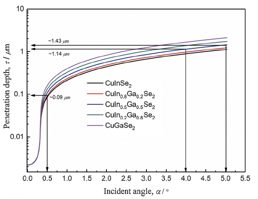
Fig. 2.
Theoretical X-ray penetration depth of the Cu(In1-xGax)Se2 (x = 0.0, 0.2, 0.5, 0.8 and 1.0) absorbing layer as a function of the incident angle.
In Eq. (2), δ is the real part of the complex refractive index and is defined as
where εo is the permittivity of vacuum (εo = 8.85 × 10⁻¹² C2/N m2), c is the velocity of light, e and m are the charge and mass of the electron, respectively, and N is the number of electrons per unit volume irradiated.
For the Cua(InbGac)Sed compound,
where ρ is the density of Cua(InbGac)Sed, Nav is the Avogadro number, Z is the atomic number, M is the molecular weight (kg/mole), and Δf’ is the real part of the dispersion correction to the scattering factor.
The parameters such as the X-ray wavelength (CuKα1, λ = 1.54056 Å), the density for CIS (ρCIS = 5.7224 g/cm3) and CGS (ρCGS =5.5640 g/cm3), the critical angle of CIS(αc_CIS = 0.321°) and CGS (αc_CGS = 0.323°), and the linear absorption coefficients of CIS (μCIS = 777.6969 cm-1) and CGS (μCGS = 414.6330 cm-1) for CuKα1 radiation were used to calculate the theoretical X-ray penetration depth of the CIGS absorbing layer [[34], [35], [36], [37], [38], [39], [40]].
As can be seen from the Eqs. (1), (2), (3), (4), the critical angle is mainly a function of wavelength, the mass attenuation coefficient, the complex refractive index, the density, the atomic number, the molecular weight, and the dispersion correction. To calculate the theoretical X-ray penetration depth for other components [Cu(In1-xGax)Se2 (x = 0.2, 0.5 and 0.8)] as a function of the incident angle, it requires the information mentioned above corresponding to each compound.
Valuesfor other factors except for density and the mass attenuation coefficient may be found in the literature. However, the density of each compound having a different composition was determined by applying the Vegard's law to the unit-cell volume or lattice parameters of CIS and CGS. The theoretical mass-absorption coefficient (μ/ρ) (cm2/g) for each compound is given by the mixture rule:
Where wi and (μ/ρ)i are the weight fraction and mass attenuation coefficient of the constituent element i, respectively. The linear absorption coefficient denoted by the symbol μ (cm-1) describes the rate of energy loss by a photon beam per centimeter within the material and is dependent on the density of the material considered and the wavelength of the X-ray radiation used.
The fraction by weight wi is given as follows:
Where Zi and Ai are the number of formula units and the atomic weight of the constituent element i, respectively.
As shown in Fig. 2, the theoretical X-ray penetration depth of the absorbing layer can be adjusted by changing the incidence angle. Hence, the GIXRD method may be applied to get structural information such as phase identifications, lattice parameters, residual stresses, etc. from the thin CIGS absorbing layer as a function of the penetration depth. The significant increase in the penetration depth occurs at the incident angle close to the critical angles due to the total external reflection of X-rays from the surface of the absorbing materials.
According to the observed GIXRD patterns as illustrated in Fig. 3, all of the diffraction peaks moved to the high angle side as the incident angle of the incoming X-ray beam increases. The shift of diffraction peaks towards higher diffraction angle implies that there is the shrinkage of a crystal lattice. These peak shifts or lattice shrinkage may occur due to the presence of stacking faults, interstitial or substitutional atoms, residual stresses, etc. on the condition that the peak shifts are not associated with the alignment of a diffractometer. Among the various factors affecting the XRD peak shifts as mentioned above, if there exist residual stresses and/or the stacking faults in the absorbing layer, they may cause the peak shift and/or broadening. However, there is a low possibility that the residual stress and stacking fault cause to the peak shifts because the CIGS sample was subjected to the post-annealing procedure at high temperature (470 °C) for a long time (60 min.), and subsequently slowly cooled down to room temperature (1 °C/min.). Hence, the degree of the peak shifts due to both the residual stress and the stacking fault may become unrecognizable in the observed diffraction pattern. As a result, they might be neglected as parameters affecting the XRD peak shifts.
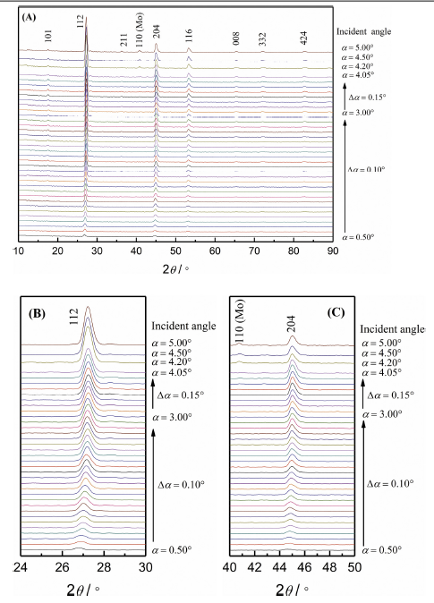
Fig. 3.
(a) Glancing incidence X-ray diffraction (GIXRD) patterns of the Cu(In1-xGax)Se2 (CIGS) absorbing layer at incident angles between 0.50° and 5.00°, (b) the shift in the position of 112 and (c) the shift in the position of 204 peak of the CIGS absorbing layer as a function of the incident angle.
As for other factors that may induce the peak shifts, the deficiency of the constituent atoms and the existence of interstitial or substitutional atoms in the crystal lattice may be considered. Here the deficiency of constituent atoms means the deviation from the ideal stoichiometric composition of the CIGS absorbing layer. As shown in Fig. 4, the EDS area mapping result from the absorbing layer shows that the average composition of constituent elements in the absorbing layer was Cu 24.93%, In 12.58%, Ga 12.31%, and Se 50.18% (at. %), respectively and the absorbing layer had the chemical composition for a near-stoichiometric CIGS. The atomic ratios between each constituent are obtained based on the average composition distribution: Ga/(Ga + In) = 0.49, In/(Ga + In) = 0.51, and Cu/(Ga + In) = 1.00. All the constituent atoms are uniformly distributed across the whole absorbing layer although the compositional gradient of In or Ga atoms perceived slightly at the front and the bottom area of the absorbing layer. Hence, the EDS results are enough not to consider the peak shift based on the deficiency of constituent atoms because the degree of non-stoichiometry of the absorbing layer becomes negligible.
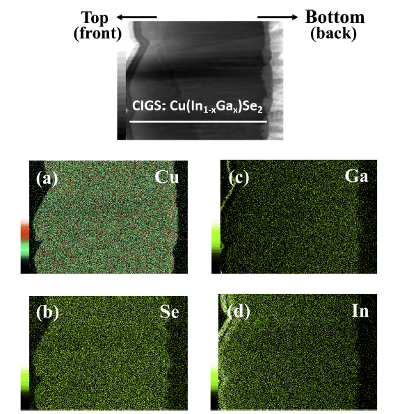
Fig. 4.
Average chemical composition of constituent atoms (Cu, Ga, Se and In) of the Cu(In1-xGax)Se2 (CIGS) absorbing layer.
Before taking the effect of interstitial and substitutional atoms on the X-ray peak shift of the absorbing layer into account, it is necessary to look through the crystal structure of the CIGS compound because interstitial atoms can occupy between the sites which are coordinated by host atoms, and substitutional ones replace the host atoms. The CIGS crystal structure belongs to the chalcopyrite type (CuFeS2) with the tetragonal crystal system (space group: I-42d (No. 122), and corresponds to two stacked zinc-blende unit cell in which one-half of the cations are replaced by Cu (Wyckoff position 4a: 0, 0, 0), and the other half by In and Ga atoms (Wyckoff position 4b: 0, 0, 1/2) [[41], [42], [43]]. Each Se is coordinated by both two In and two Cu atoms (Wyckoff position 8d: x, 1/4, 1/8) and each of these cations is tetrahedrally coordinated by four anions.
There are only two sites, (Wyckoff position 16e: x, y, z) and (Wyckoff position 8c: 0, 0, z) available assuming that the three cations (Cu, In, and Ga) and one anion (Se) filled the sites mentioned above in space group I-42d (No. 122). If some atoms are introduced into the CIGS compound as interstitial atoms and occupy any of two sites or both sites, the diffraction pattern is completely different from the calculated one based on the crystallographic information described above even though these sites have low occupancies.
When taking both In and Ga atoms co-occupy the same crystallographic site (4b site: 0, 0, 1/2) in the ideal CIGS compound into consideration, the degree of the peak shift will depend on the relative content of In or Ga as well as the difference between the ionic radius of In3+ (0.80 or 0.81 Å) and Ga3+ (0.62 Å) [[44], [45], [46]]. The difference of the ionic radius between two cations is enough to change the interplanar spacing, which is the perpendicular distance between two successive planes. The interplanar spacing is also a function of the unit-cell parameters for seven crystal systems and can be expressed to Miller indices, h, k, l, which fully describe every set of crystallographic planes.
In order to collect the GIXRD data from only the absorbing layer except for the front top layers (TCO and CdS) in the CIGS solar cell, the surface layers were removed with a mixture of HNO3 and HCl solution with the ratio of 1:3 and then the GIXRD experiment was carried out the depth-profile only for the absorbing layer. As shown in Fig. 3, the GIXRD patterns of the absorbing layer were identified as the CIGS single phase. The diffraction patterns taken from low incident angles correspond to the surface of the top region of the absorbing layer, and the ones by high incident angles represent the Mo layer near the substrate. By increasing the glancing incident angles from 0.50° to 5.00° (X-ray penetration depths of ∼0.09 to ∼1.43 μm estimated from the Fig. 2), the overall intensities of diffracted peaks gradually increase and the peaks indicating the Mo phase become noticeable. Of the observed peaks, the diffraction line from the lattice plane (110) at 2θ = ∼41.5° indicates the Mo reflection of the cubic phase. The X-ray diffraction peaks corresponding to the MoSe2 phase, which was observed at the cross-sectional TEM image of Fig. 1, could not find at the collected diffraction patterns because when compared with the content of other phases in the CIGS compound, the relative MoSe2 phase content is very small although the incident X-ray beam is enough to irradiate the region of the MoSe2 phase.
In Fig. 3, all reflection peaks including two representative 112 and 204 peaks of CIGS at 2θ = ∼ 27.1° and 2θ = ∼ 45.1°, respectively, gradually move to higher values of 2θ when the incident angle increases up to ∼3.50°, whereas the degree of the peak shifts to the high angle side is small below the incident angle of 5.00° without showing other phases. When the incident angle increases, the peak shift in XRD towards the higher angle side. This observation may be closely related to the result of the change in the site occupancy of constituent atoms having a different ionic radius. The difference in their ionic radii (In3+: 0.80 or 0.81 Å, Ga3+: 0.62 Å) is enough to induce the peak shift in the X-ray diffraction pattern. Consequently, among the factors affecting the XRD peak shift as mentioned above, the X-ray peak shift observed at the CIGS absorbing layer is mainly caused by the relative content of In or Ga atoms which co-occupy the same crystallographic site [4b site at (0, 0, 1/2)].
The fact that the XRD peak shifts to higher angle with increasing the incident angle, which corresponding to the shrinkage of the interplanar distance of the absorbing layer, means that the relative site-occupancy ratio of Ga to In atoms occupying the same site is gradually changed from the surface to the bottom region. Since the peak shift in XRD is surely a result of the change in the lattice parameters, this result suggests that the distribution of In or Ga with depth in the absorbing layer may be determined by the precise measurement of the lattice parameters based on data collected by the GIXRD technique.
There are a number of methods to refine the lattice parameters based on X-ray diffraction data, such as Pawley, Le Bail, Rietveld refinement, and so on. The Rietveld method requiring an initial structural model is that all structural and instrumental parameters are refined by fitting a calculated profile to the observed diffraction data without extraction of the individual integrated intensities from X-ray powder diffraction data, while the Pawley and Le Bail methods using only knowledge of the lattice parameters and the space group can allow refining lattice parameters and extracting peak intensities from X-ray powder diffraction data. Of the two methods, the Pawley requires fewer least-squares cycles for convergence and is slightly faster.
Among these methods, the Pawley refinement was used to refine the lattice parameters of the absorbing layer as functions of depth. The Pawley refinement requires information about the lattice parameters and the space group describing the crystal structure of CIGS as initial parameters. The space group I-42d (No. 122) and the lattice parameters reported in the literature were used as the initial values [[41], [42], [43]].
Before fitting the initial structural model to GIXRD data, the zero-point shift value for the collected GIXRD diffraction data was corrected with a standard reference material (SRM) 640c (NIST) [47]. Subsequently, the peak-profile function parameters including peak asymmetry were refined. As a result of the Pawley refinement, all reflection peaks observed from the CIGS absorbing layer could be indexed by crystallographic information based on the initial crystal model. Finally, the lattice parameters of the absorbing layer were refined as functions of the incident angle. Fig. 5 shows both the lattice parameters (a and c) and the unit-cell volume as a function of the incident angle, respectively. By increasing the incident angle, the lattice parameters (a and c), and the unit cell volume gradually decreased at the incident angle of 3.5°, and then was held nearly steady until 5.00°.
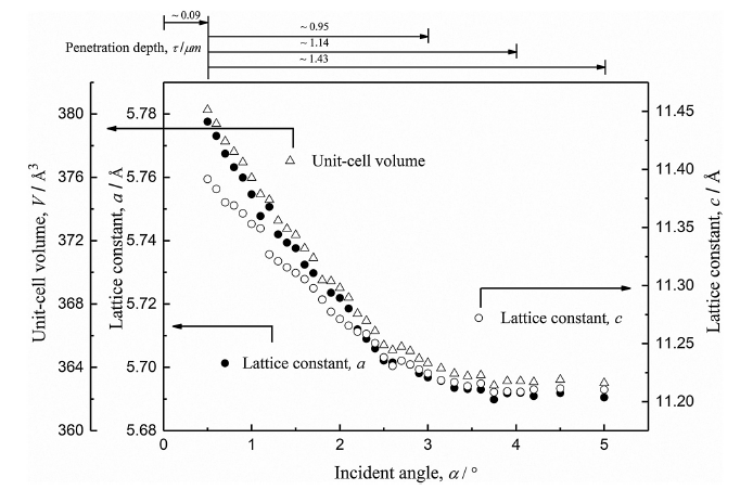
Fig. 5.
Lattice parameters (a and c) and unit-cell volume of the Cu(In1-xGax)Se2 (CIGS) absorbing layer as functions of the incident angle.
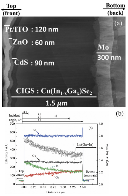
Fig. 6.
(a) Cross-sectional transmission electron microscope (TEM) photograph and (b) compositional profile of constituent atoms (Cu, Ga, Se and In) of the Cu(In1-xGax)Se2 (CIGS) absorbing layer as a function of depth from the surface to the bottom of the absorbing layer.
When the incident angle was increased from 0.50 to 5.00°, the refined a and c lattice parameters of the absorbing layer were decreased from 5.7776(3) to 5.6905(2) Å, and 11.3917(3) to 11.2114(2) Å, respectively. Also, the corresponding unit-cell volume was gradually decreased from 380.2625(3) on the surface to 363.0452(2) Å3 on the bottom region. The number in parenthesis is the uncertainty of the refined lattice parameters or the refined unit-cell volume. When considering that the X-ray peak shift observed at the CIGS absorbing layer is mainly caused by the relative content of In or Ga atoms in the same site [4b site at (0, 0, 1/2)], the fact that both the lattice parameters and the unit-cell volume decrease as the penetration depth increase, correspondingly increase as a function of the incident angle indicates clearly that vertical variation in composition of In and Ga with depth inside the absorbing layer exists.
The brightness of colour in the EDS results of Fig. 4 exhibits the distribution of the individual chemical constituents (Cu, In, Ga and Se) in the absorbing layer. Approximately, the same brightness of colour in Fig. 4a and b represents that both the Cu and Se atoms were uniformly distributed from the top to the bottom region. In contrast, the brightness of colour indicating the distribution of Ga and In atoms in Fig. 4c and d was found slightly non-uniform across the whole area. The depth-dependent brightness variation implies that there exists the compositional gradient of In and Ga atoms in the absorbing layer.
Fig. 6 shows the chemical composition profile for each constituent from the surface of the absorbing layer as a function of depth. According to the compositional profile results, while the chemical composition profiles of Cu and Se exhibited small fluctuations from the surface to the bottom region, the content of In gradually decreased from the surface; the opposite trend was observed in Ga. This result ensures that the atomic ratio between In and Ga in the absorbing layer is depth-dependent. The compositional gradients of In and Ga appeared on the surface of the absorbing layer nearly disappeared at ∼ 1.2 μm in depth. Also, Se markedly increased at the interfacial region between the CIGS and the SUS substrate layers due to the MoSe2 phase formation as identified in Fig. 1. This chemical composition gradient of In or Ga in the absorbing layer is consistent with the change of the lattice parameters (or the unit-cell volume) with depth as shown in Fig. 5. As shown by both GIXRD and EDS results, when the incident angle increases, the lattice parameters decrease, whereas the content of Ga increases; the content of In decreases. This behaviour is due to the relative site occupancy of Ga or In sharing the 4b site as well as the difference between the ionic Pauling size of the In3+ (0.80 or 0.81 Å) and Ga3+ (0.62 Å) cations tetrahedrally coordinated by the anions [[44], [45], [46]].
The electronic properties of the CIGS thin-film solar cells are strongly related to their compositional fluctuation along with inherent defects in the absorbing materials. The compositional fluctuation inside the absorbing layer with depth is similar to the depth profile of the constituent atoms. In the CIGS crystal structure having stoichiometric compositions, replacing Ga with In yields for continuous change in the bandgap of the CIGS absorbing layer that varies from ∼1.0 (CIS) to ∼1.7 eV (CGS) [[9], [10], [11], [12]]. Wei et al. suggest an empirical model for describing the bandgap, Eg(x) of CuIn1-xGaxSe2 by varying the composition x as follows [10]:
where Eg(x) and x are the bandgap and the Ga/(Ga + In) ratio in the CIGS absorbing layer, respectively.
From this equation, we find that the variation of the bandgap can be expressed as a function of the unit-cell volume based on the use of the so-called Vegard’s law [48]. The Vegard’s law assumes that the volume of unit-cells in a substitutional solid solution is linearly proportional to the fraction of sites substituted. When the Vegard’s law is applied to the CIGS absorbing layer of which the unit-cell volume was changed from 380.2625(3) on the surface to 363.0452(2) Å3 on the bottom region, the bandgap variation ranged between 1.222 and 1.532 eV from the surface to the bottom layer. This indicates that both the stoichiometry and electronic properties of the CIGS absorbing layer are graded with respect to depth. As clearly seen in Fig. 7, the change of the absorbing layer’s bandgap is consistent with both the variation of both the unit-cell volume (or the lattice parameters) and the chemical profile of In or Ga as a function of the incident angle. Moreover, as the unit-cell volume (or the lattice parameter) of the absorbing layer decreases, its bandgap becomes higher. This can be understood that, if the lattice parameters are decreased, the interatomic distance will be reduced, and binding energy between the valence electrons and the host atoms will be increased. Consequently, the bandgap of the absorbing layer becomes wider. In Fig. 7, the penetration depth of the incident X-ray beam as variation in the composition of In and Ga with depth inside the absorbing layer was calculated based on the result of the chemical composition profile (Fig. 6) and the Eqs. (1), (2), (3), (4). The penetration depth gradually increased as the incident angle increased.
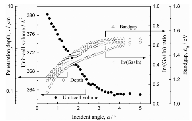
Fig. 7.
Unit-cell volume, theoretical penetration, In/(Ga + In) ratio and bandgap of the Cu(In1-xGax)Se2 (CIGS) absorbing layer as functions of the incident angle.
The lattice parameters gradient corresponding to the non-uniform Ga/In ratio or compositional gradient in the absorbing layer may allow the bandgap of the CIGS absorbing layer to be graded. The bandgap grading may influence the collection and recombination of photocarriers in the absorbing layer. Although the bandgap of the absorbing layer is not the only factor, which can affect the cell performance, the cell with the lattice parameters gradient, leading to the bandgap grading in the CIGS absorbing layer may represent higher the CIGS solar cell performance in comparison with the cell that has the uniform bandgap of the absorber layer because the absorber layer having the graded bandgap enhances carrier collection for longer-wavelength photons and reduces carrier recombination at the heterojunction and back regions of the cell.
This approach may be applied to nondestructively estimate the bandgap grading of the absorbing layer. Furthermore, it may provide a means to characterize the bandgap depth profiling on A1-xBx compounds regardless of the compositional analysis through the refinement of the lattice parameters using GIXRD data, which can be collected by changing the incidence angle of incident X-ray beam into the sample.
4. Conclusion
The depth profile of the unit-cell volume (or the lattice parameters) of the CIGS absorbing layer obtained from the Pawley refinement based on diffraction data recorded in GIXRD geometry was compatible with the result of the chemical composition depth profile of the CIGS absorbing layer using the cross-sectional EDS analysis. The result of this study, drawing the relationship between the lattice parameters or the unit-cell volume depth profile and the composition gradients of In or Ga in the CIGS absorbing layer based on the GIXRD technique, provides an alternate way to nondestructively estimate the bandgap gradients of the CIGS absorbing layer.
Reference

 WeChat