

1. Introduction
Toluene (C7H8) is an important industrial compound and intensively employed for synthesizing other chemical intermediates such as adhesives, cosmetics, solvents, pharmaceuticals, dyes, medicines, agricultural chemicals, explosive and a constituent of fuels. It is produced traditionally from coal or crude oil by fractional distillation [[1], [2], [3], [4]]. Recently, toluene industrial production has been realized by alkylation of the methanol-benzene system with the aid of a catalyst and generally operating at about 400 °C to obtain a high yield of toluene [5,6]. On the other hand, toluene can also leak during production, which becomes hazardous emission to both human health and environment owing to its high volatility, especially for the most vulnerable object such as toluene-related industrial production workers, air, and groundwater quality in the nearby area. It can cause several acute diseases for longtime exposure to humans, such as headaches, nausea, skin irritation, etc. [[7], [8], [9]]. In this regard, to monitor leak probability and minimize the harmful effect of toluene emission for both humans and the environment, it should be detected immediately before reaching to open air. However, advanced researches regarding the toluene sensor are generally aiming for outdoor and indoor toluene gas monitoring from household uses such as paint, thinner, cigarette, adhesive, gasoline, and so on, which could be operated at room temperature [[10], [11], [12]]. To the extent of our knowledge, a toluene gas sensor for a high-temperature application that can be employed during toluene production is rather less attempted.
Toluene gas sensing materials based on metal oxide semiconductors (MOS) have been extensively studied due to their facile synthesis, and nanostructurization of MOS (1-100 nm) can lead to an increase of gas sensing performance due to nanosized effects [13,14]. For example, nanomaterials possess a high specific surface area, which provides an abundant site for gas adsorption [14]. Additionally, nanoparticles serve better surface contact for electrons and/or holes transport in their interparticle [15]. Tin (IV) oxide (SnO2), one of the transition metal oxides, is the most well-known gas sensing material, and recent studies about nanostructures of SnO2 have shown its responsivity to toluene at high temperature (above 350 °C [16,17]. For further improvement of SnO2 gas sensing properties, decoration with other materials has been reported. There are two types of composite formation; (i) noble metals and (ii) p-type semiconductors. (i) Loading with noble metal nanoparticles such as Au, Ag, Pt or Pd can effectively enhance its toluene gas sensing property. For example, SnO2 decorated with Pd nanoparticle, improved their responsivity as well as selectivity because of the “spill-over” effect that bring much active sites for oxygen species and strengthen adsorption energies (Eads) between target gas and sensing material [[18], [19], [20], [21], [22]]. Actually, (ii) addition of p-type to n-type will create p-n junction at particle interface that will consequently increase charge carrier concentration, modify band-gap structure, and inhibit charge recombination. Thus, decoration of n-type SnO2 with p-type counterparts should contribute largely to the enhancement of gas sensing performance as compared to a single n- or p- component [[23], [24], [25]]. While utilization of noble metals hinders sensor devices from cost-effective fabrication, copper (II) oxide (CuO) can lead to the preparation of cost-effective sensors due to its abundance. Therefore, a p-n junction CuO/SnO2-based gas sensing material is expected to be developed for practical applications. Conventionally, p-type CuO/n-type SnO2 combination has been and is still being explored for its utility to detect H2S gas [[26], [27], [28], [29]]. However, investigation of CuO/SnO2 for high temperature toluene gas sensing property is still less pronounced but profoundly needed.
In the present research, we report on a successful uniform decoration of a spherical SnO2 with CuO nanoparticles at room temperature, enabling the time-effective and energy-saving process and scaling-up to the industrial level. We found that electrostatic force interaction occurred at the surface between positively charged CuO and negatively charged SnO2 has led to this uniform self-decoration. With the utilization of different mixed organic solvents in solvothermal synthesis, the surface charge of metal oxides can be controlled. The prepared CuO-decorated SnO2 demonstrated an excellent toluene gas sensing performance in the term of response and selectivity even at high temperatures which is mainly attributed to p-n heterojunction, ohmic junction and spill-over effect due to the partially reduced CuO to Cu metal nanoparticles during the introduction of reducing gas that has a similar phenomenon with addition of Pd or Pt metal nanoparticles. We also systematically proposed the gas sensing mechanism of electrostatic self-decoration.
2. Experimental section
2.1. Preparation of CuO nanoparticles and spherical SnO2
All chemicals in the experiments were purchased from FUJIFILM Wako Pure Chemicals Corporation, analytical grade, and utilized without additional treatment. CuO nanoparticle was prepared using a solvothermal method by modifying a reported study [30]. In the mentioned report, 50 ml of copper acetate alcoholic solution was utilized. In our synthesis process, 0.3 mmol of anhydrous copper acetate (Cu(OAc)2, 97.0 %) was dissolved in 30 ml dehydrated ethanol (EtOH, 99.5 %). A transparent light green solution was obtained after stirring 500 rpm for 30 min at 50 °C. Then, the solution was transferred to 100 ml Teflon-lined autoclave and treated at 150 °C for 20 h. The black precipitate was collected by vacuum filtration and washed with ethanol several times and placed inside a depressurized drying oven at 70 °C for 12 h.
To synthesize spherical SnO2, a newly developed-technique, namely water controlled-release solvothermal process (WCRSP), was utilized [17]. The synthesis method started by dissolving 1 mmol of anhydrous tin chloride (SnCl2, 99.8 %) in 40 ml of dehydrated ethanol. The solution was stirred at 400 rpm for 30 min. Subsequently, 10 ml of acetic acid (HOAc, 99.7 %) was added dropwise and the solution was maintained under the same stirring condition for another 30 min. Then, the solution was moved into a 100 ml Teflon-lined autoclave and heated for 20 h at 200 °C. After the system cooled to room temperature, the obtained powder was washed with ethanol followed by vacuum drying at 70 °C for 12 h.
2.2. Preparation of CuO nanoparticles decoration on spherical SnO2
A simple preparation method of a uniform CuO nanoparticles decoration on spherical SnO2 (SnO2@CuO) was designed. 0.1 mmol of the prepared CuO nanoparticles were dispersed in 10 ml ethanol and placed in ultrasonic bath for 30 min to obtain a homogenous solution. Then, 0.5 mmol of the obtained spherical SnO2 was added to the solution containing CuO nanoparticles, and the mixture was stirred for another 30 min and recovered by filtration. After drying at 70 °C, the SnO2@CuO was crushed by agate mortar. To reveal the effect of amount of CuO nanoparticles decoration on gas sensing properties, SnO2@CuO samples with variation amount of CuO nanoparticles (0.05, 0.2 and 0.3 mmol) were also prepared.
2.3. Characterizations
The phase structure of each sample was analyzed by using X-ray diffraction (XRD, Bruker AXS D2 PHASER with CuKα radiation = 1.5418 Å). Field emission scanning electron microscopy (FE-SEM, Hitachi S4800), transmission electron microscopy (TEM, JEOL JEM-2010) and scanning transmittance electron spectroscopy (STEM, JEM-ARM200F) were utilized to observe the morphological feature, lattice parameter and elemental distribution mapping of the synthesized samples. The surface electronic state, chemical composition and bonding characteristic were identified by X-ray photoelectron spectroscopy (XPS, ULVAC PHI5600). The UV-vis diffuse reflectance spectra (DRS) of obtained samples were collected by UV-vis spectrophotometer (JASCO V-670 Spectrophotometer). The effective electric surface charge of particles was determined by Zeta potential measurement (Malvern, Zetasizer Nano ZS). N2 adsorption/desorption (Quantachrome, NOVA 4200e) measurement was performed to calculate specific surface area and pore size distribution. The solvent mixture after the solvothermal reaction was investigated by nuclear magnetic resonance (1H NMR, Varian Unity Inova, 500 MHz).
2.4. Gas sensor fabrication and measurement
The following process described sensor device preparation. A commercially available Au-based interdigitated electrode was combined with a borosilicate glass holder by pasting a silver slurry at each end of the electrode accompanied by annealing at 400 °C for 30 min [31]. Then, the prepared samples were mixed with ethanol to form a homogeneous slurry and then this slurry was coated onto an electrode until it was fully covered. The gas sensing performance of the samples was evaluated using a two probes method in a home-design gas sensing analysis equipment (Agilent 34420A, 100 Ω-100 MΩ and switch unit Agilent 34970A) based on Taguchi Gas Sensor (TGS) with the static system. The sensing measurement was conducted at the varied temperature ranging from 200 °C to 450 °C to determine the optimum working temperature where the sensor material exhibited the highest responsivity to toluene gas, as it is essential for the practical use. Initially, the sensor devices were exposed to ambient air at desired temperatures and kept about 45-60 min until the sensor resistance reaches a stable value. At this point, the measured resistance was named as resistance in the air (Ra). The condition was maintained for 10 min and then the target gas was injected, eventually led to the change in the sensor resistance. At this condition, the recorded resistance was denoted as resistance in gas (Rg). The sensor response in a reducing gas mixture was calculated as Ra/Rg for n-type semiconductor or Rg/Ra for p-type semiconductor. The sensors were also exposed to other reducing gases such as hydrogen, methanol and ethanol to examine its selectivity. After the measurement, the sensor robustness was characterized by SEM and XPS to observe the changing on the phase, chemical composition and morphological structure of the sensing material.
3. Results and discussion
3.1. Structure and morphology of CuO nanoparticles, spherical SnO2 and SnO2@CuO
The XRD patterns of the CuO nanoparticles, spherical SnO2 and SnO2@CuO are compared in Fig. 1. In the XRD pattern of the CuO nanoparticles (Fig. 1(a)), all the appeared peaks were originated to 110, 002, 111, -202, 020, -113, 022, 220, 311, and 004 diffractions of CuO with monoclinic phase, being in good agreement to the standard pattern (JCPDS 48-1548). While for the spherical SnO2 (Fig. 1(b)), the peaks could be assigned to tetragonal rutile-type SnO2 (JCPDS 77-447). Furthermore, no characteristic peaks related to other phases in both XRD patterns indicated the obtained samples had no impurity. As shown in Fig. 1(c), after the SnO2 decoration treatment, the emerged peaks only belong to SnO2, or in other words, the monoclinic phase of CuO was not detected in SnO2@CuO sample due to the low amount of CuO. However, in the case of the higher amount of CuO nanoparticles (0.3 mmol), the 002 and 111 peaks started to be appeared (see XRD patterns in Fig. S1), demonstrating necessary amount to detect CuO phase in SnO2@CuO system should at least 0.3 mmol. All the prepared samples had broadened peaks, suggesting their nanocrystalline property. According to the Debye-Scherrer formula, D = Kλ/βcosθ [32], where K is crystallite-shape factor with value of 0.9, λ is the used X-Ray radiation, β is full width at half-maximum (FWHM, radians) and θ is Bragg angle (degree), the crystallite sizes (D) of SnO2 (110) and CuO (111) were estimated to 4.1 nm and 6.9 nm, respectively.

Fig. 1.
XRD patterns of (a) CuO nanoparticles, (b) Spherical SnO2 and (c) SnO2@CuO.
The morphological feature, crystal structure and elemental distribution were investigated by TEM, corresponding selected area electron diffraction (SAED) patterns, high-resolution TEM (HRTEM) and electron diffraction spectroscopy (EDS) mapping. Fig. 2(a) represents the TEM observation of the pure CuO, and the inset is the corresponding SAED patterns The TEM image clearly shows that the CuO consists of spherical nanoparticles with an average size of about 7 nm, being consistent with the estimated number obtained from the XRD results. Furthermore, as shown by the SAED patterns (inset), the diffuse diffraction rings are corresponded to the 110, 002, 111, -202, 202 and -113 diffractions of CuO, confirming the polycrystalline property of the obtained CuO nanoparticles. Additionally, the HRTEM image in Fig. 2(b) demonstrates a lattice space of 0.27 nm which corresponds to the (111) plane of monoclinic phase CuO, which is in agreement with its XRD pattern. Considering that no other d lattice spacing, the CuO nanoparticles may possess single-crystalline property. Fig. 2(c) shows the TEM image of SnO2. It showed the spherical morphology of the obtained SnO2. The average size of spherical SnO2 was about 1.2 μm, and the corresponding SAED pattern depicted in the inset suggests that the spherical SnO2 also possessed a polycrystalline feature. The diffraction rings could be assigned to 110, 101, 200, 211 and 002 diffractions of tetragonal rutile-type SnO2. Based on our previous results [17], the spherical morphology was actually constructed by many interconnected nanoparticles which their presence can be confirmed by HRTEM image shown in Fig. 2(d). It was clear that interplanar lattice distance of 0.33 nm was corresponding to the 110 diffraction of tetragonal rutile-type SnO2, confirming that SnO2 nanoparticles might be a single crystal, although the spherical structure was polycrystalline. Fig. 2(e) displays the TEM observation of SnO2 after CuO decoration. As seen in the TEM images, its morphology was similar to that of the parent morphology of the SnO2. As expected, the spherical morphology observed in the TEM images of the SnO2@CuO sample was verified to be SnO2 as SAED pattern shown in the inset indicates the diffraction rings of tetragonal rutile-type SnO2 with 110, 101, 200, 211 and 002 diffractions. The SAED patterns were also in good agreement with SAED pattern of the bare SnO2, inferring that the decorative nanoparticles had no effect on the tetragonal crystal structure of SnO2. From Fig. 2(e), it could also be observed that the spherical SnO2 was surrounded by a massive number of nanoparticles after CuO decoration. The HRTEM presented in Fig. 2(f) identified the lattice fringes of the surface of the SnO2@CuO sample. Two different lattice spaces with d values of 0.33 nm and 0.27 nm were observed, which were attributed to the 110 diffraction of tetragonal SnO2 and 110 diffraction of monoclinic CuO, respectively. Moreover, the nanoparticles of CuO had intimate contact with SnO2 particles, forming p-n heterojunction which was presumed to be beneficial for the gas sensing response.

Fig. 2.
TEM images (inset is ED pattern) and the corresponding HRTEM image of (a, b) CuO nanoparticle (c, d) spherical SnO2 (e, f) SnO2@CuO. (g) Dark-field image and elemental mapping of (h) Sn (i) Cu (j) O and (k) EDX profile of SnO2@CuO.
To examine the nanoparticles distribution of the CuO on the surface of spherical SnO2, STEM and EDS mapping were conducted. DF-STEM images of the SnO2@CuO shown in Fig. 2(g) revealed gradient in contrast where middle region of the spherical SnO2 was denser than the outer surface. Fig. 2(h-j) show the elemental mapping of each individual element, demonstrating Cu, Sn, and O elements were homogeneously distributed throughout the whole observe region. The results strongly supported that CuO nanoparticles were well-decorated on the surface of spherical SnO2, creating p-n junction which might play as a carrier regulator for the improvement of toluene gas detection. The EDS profile (Fig. 2(k)) from selected area (blue circle) of SnO2@CuO confirmed the existence of Cu, Sn and O elements. Additionally, the detected Ni signals were associated to Ni grid. The measured atomic percentage of Cu, Sn, and O were 4.3, 36.5, 59.2 %, respectively.
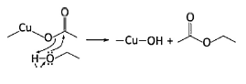
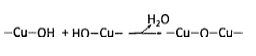
1H NMR analysis for the filtrates after the solvothermal reaction and the following collection of the precipitate by vacuum filtration was conducted to propose a possible formation mechanism of CuO nanoparticles and spherical SnO2. Fig. S2 (Supplementary information) displays the 1H NMR spectrum of the final solution from the CuO synthesis using copper acetate as a precursor and dehydrated ethanol as a solvent. The 1H NMR spectrum showed triplet peaks at 1.146 ppm-1.177 ppm (CH3CH2OH) and quartet peaks at 3.569-3.612 ppm (CH3CH2OH), indicating the existence of residual ethanol after the reaction. Additionally, the last singlet peak located at 4.890 ppm corresponded to water molecule (H2O) [33]. From the 1H NMR result, the presence of water molecule directly pointed to reaction mechanism during the treatment. Similar fashion had been studied by Joo et al. [34] utilizing zinc acetate and octyl alcohol to synthesize zinc oxide nanocrystal. They proposed a mechanism so-called ester elimination reaction and proved the presence of ethyl acetate detected by GC-FID. Similar to their work, CuO formation in this study is predicted by following steps: (1) Lewis acid enabled-nucleophilic oxygen attack to acetate ligand due to the lack of electron density and (2) CuO and in situ water are generated through polycondensation of Cu(OH)2. It was noted that even though ethyl acetate should be formed during chemical process as shown in step (1), it was not presence in NMR, which might be caused by very low amount of ethyl acetate in final solution considering the amount of precursor was only 0.3 mmol. Additionally, NMR might less sensitive than GC-FID.
In the case of spherical SnO2, the formation mechanism had been reported in our earlier study [17]. In brief, the 1H NMR study clarified the existence of ethyl acetate (CH3COOCH2CH3) in addition to the ethanol solution. The ethyl acetate was an esterification product between ethanol and acetic acid during solvothermal condition and at the same time, the water molecule was slowly generated. These water molecules hydrolyzed the SnCl2 precursor to induce nucleation and crystal growth to form SnO2 nanoparticle subsequently. The nanoparticle finally aggregated to build a spherical structure with spherical morphology as it had been confirmed by the TEM observation (Fig. 2). It was found that the size of sphere largely depended on the volume ratio of ethanol/acetic acid, solvothermal reaction time, temperature process and precursor concentration. There were also other compounds detected in 1H NMR, such as diethyl ether (CH3CH2OCH2CH3) and hydrochloric acid (HCl), indicating the dehydration yields of ethanol and by-product from SnCl2 hydrolysis.
We performed zeta potential analysis to determine charged particles and clarify the reason for the excellent contact between p-type CuO nanoparticles decoration and n-type spherical SnO2. As depicted in Fig. S3(a, b), CuO nanoparticles surface possessed positively charged (22.9 ± 4 mV), while spherical SnO2 surface had negatively charged (-3.39 ± 1.3 mV). The positive charge of CuO nanoparticle might be originated from adsorbed ethanol during the solvothermal treatment, as it was well-accepted that ethanol was a protic solvent that had positive charge from a labile (H+). This was different from that of synthesis for spherical SnO2, which utilized SnCl2 as precursor and esterification-induced ethyl acetate production beside ethanol solvent. Small fraction of Cl- might remain on SnO2 surface, giving a negative charge on its surface. Moreover, ethyl acetate was aprotic solvent where the two oxygen atoms on carbonyl and ethyl groups had a highly electronegative charge. It was inferred, from these results, the electrostatic force interaction induced a uniform CuO nanoparticle decoration on SnO2 spherical surface.
To analyze the core level surface electronic state of the synthesized samples, the XPS analysis was performed. A full scan XPS spectra of pure SnO2 and SnO2@CuO are shown in Fig. 3(a). The result confirmed the strong spectra of Sn and O element in the pure SnO2 and the addition of Cu element in SnO2@CuO. In Fig. 3(b), the Sn3d peaks of both pure SnO2 and SnO2@CuO were compared. The symmetrical doublet peaks located at 495.1 and 486.6 eV were assigned to Sn 3d3/2 and Sn 3d5/2 levels, respectively. These peaks were corresponded to Sn4+ state of Sn in tetragonal rutile-type SnO2 [35]. After the CuO nanoparticle decoration, the peaks had been slightly shifted to lower binding energies of 494.9 eV for Sn 3d3/2 and 486.5 eV for Sn 3d5/2.Fig. 3(c) displays the O1s XPS scan of pure SnO2 and SnO2@CuO. The O1 s spectra in both samples consisted of overlapping components, and they were fitted with Gaussian function to obtain resolved peaks. The binding energy peaks from 531 to 530.5 eV were related to oxygen binding to Sn4+ in metal oxide lattice, while for the peaks around 532.2-531.9 eV were referred to an atmospheric carbon-oxygen related compound adsorbed on the SnO2 surface. The high-resolution Cu 2p scan depicted in Fig. 3(d) shows four peaks centered at 933.4, 942.2, 953.3, and 962 eV. The peaks at 933.3 and 953.3 eV could be ascribed to Cu 2p3/2 and Cu 2p1/2, respectively. These peaks showed the feature of Cu with the oxidation state of 2+, further confirming the presence of CuO phase in the SnO2@CuO system. The remaining peak observed at 942.2 eV was the satellite peaks of Cu 2p3/2 and 962 eV was for Cu 2p1/2 satellite peak. These satellite peaks appeared due to a partially filled 3d9 orbital in Cu2+ state [36]. It was noteworthy to mention the peak shift in Sn 3d, O1s and Cu 2p core-level spectra after decorating with CuO nanoparticles, which might be contributed by a weak bonding between components in SnO2@CuO, such as Cu-SnO-bond similar to that in CuSnO3 material where Sn 3d, O 1s and Cu 2p exhibited a slight shift toward lower binding energy [37]. The EDS and XPS results convinced the attachment of CuO phase on the spherical SnO2 surface. We also found a small fraction of Cl (0.93 at. %) originating from SnCl2 precursor used in SnO2 synthesis, though this Cl effect on gas sensing properties were negligible [17].

Fig. 3.
(a) XPS spectra of SnO2@CuO sample. (b-d) High-resolution spectra of Sn 3d, O 1s and Cu 2p, respectively.
The nitrogen adsorption-desorption analysis had been performed to give further insight into the textural properties of CuO nanoparticles, spherical SnO2 and SnO2@CuO. The N2 isotherm and corresponding Barret-Joyner-Halenda (BJH) pore size distribution plot (inset) derived from desorption data are demonstrated in Fig. 4. According to the IUPAC classification, all the isotherms were classified into type IV with a hysteresis curve at 0.4-0.9 of relative pressure (P/Po), suggesting the existence of porosity. As calculated by BJH method, all the samples exhibited an average pore size of 1.9 nm and small mesopores of 3.2 nm for the CuO nanoparticles sample. The micro-/mesopores had also been observed in TEM images (Fig. 2), which probably due to unfilled space between the attached nanoparticles. Additionally, the SnO2 sample presented the highest specific surface area of 113 m2/g. After the decoration with CuO nanoparticles, the specific surface area slightly decreased to 107 m2/g because the CuO had a lower specific surface area (90 m2/g) than that of the SnO2.

Fig. 4.
N2 isotherm graph and inset is pore diameter of (a) CuO nanoparticles, (b) spherical SnO2 and (c) SnO2@CuO.
Optical properties of the p-type CuO and n-type SnO2 obtained from non-hydrolytic technique were characterized by UV-vis diffuse reflectance spectra to predict band gap structures that will be utilized in proposing the gas sensing mechanism of p-n junction based sensor material. As shown in Fig. S4, it was observed that the absorption edge of CuO (925 nm) was much longer than that of SnO2 (421 nm), reflecting CuO had a narrower band gap energy, which was calculated using a well-known Tauc’s formula : (F(R)hν)1/n = A(hν - Eg), where F(R) is Kubelka-Munk equation, h is Planck’s constant, ν is the frequency of vibration, α is absorption coefficient, A is proportional constant and Eg is band gap. The estimation of band gap can be obtained from the intersection of (F(R)hν)1/n plot with the vertical axis. By assuming direct allowed transition (n = 1/2), the estimated band gap of CuO nanoparticle and spherical SnO2 in this study were 1.5 eV and 3.1 eV, respectively, in which these values were far from an ideal band gap of bulk CuO (1.2 eV) or SnO2 (3.6 eV) that might be caused by carbon or chlorine doping originated from organic solutions and precursors during solvothermal treatment.
3.2. Gas sensing properties of CuO nanoparticle, spherical SnO2 and SnO2@CuO
3.2.1. Effect of CuO nanoparticles decoration on gas sensing performance of SnO2@CuO
Gas sensing response towards 75 ppm toluene gas as a function of working temperature was thoroughly investigated. As shown in Fig. 5(a), the toluene sensing performance of spherical SnO2 was significantly enhanced by the decoration of CuO nanoparticles compared with the decoration material itself, meaning that the improved sensing response was affected by synergistic performance of p- CuO and n- SnO2 creating p-n heterojunction. Especially, the toluene sensing response of SnO2@CuO started to increase at above 300 °C and reach the highest sensing response (S = Ra/Rg) value of 540 at its optimum working temperature of 400 °C, which was about 100 times greater than the pure SnO2 or CuO. At higher temperature above 400 °C, the sensing response decreased gradually. It is well-documented that surface reaction based on kinetic adsorption-desorption of oxygen species with sample gas on sensing material should be the reason for this phenomenon [[38], [39], [40]]. At relatively low working temperature, the oxygen adsorption was more dominant than that of desorption, leading to a lower reaction between tested gas and oxygen ion species and insufficient response. The balance of oxygen adsorption-desorption process was attained at their best operating temperature at which the material exhibited the highest sensing response. Oxygen desorption became more dominant at further high temperature, therefore the adsorb oxygen species was not enough to complete reaction with detecting gas. Generally, there are two types of semiconductor gas sensing, i.e., n-type and p-type. In reducing gases environment, sensor resistance of n-type semiconductor reduces during gas exposure and increases during gas release, while p-type shows a contrary characteristic [41]. In Fig. 5(b-d), pure CuO and SnO2 showed typical p-type and n-type property, respectively and even after decoration of CuO, SnO2@CuO exhibited similar characteristics with the parent n-type SnO2. This was due to a relatively low amount of decorative material. However, we observed a remarkable change in the base sensor resistance of SnO2@CuO sample. For example, the decorative material CuO showed the lowest resistance (∼250 Ω) and parent material SnO2 possesses an intermediate value of resistance (∼200 kΩ). When decorating material was added to spherical SnO2, the resistance greatly increased to ∼15 MΩ, which was about 75 times higher than SnO2 before decoration. It was also observed that the response time of SnO2@CuO (100 s) was shorter than those of pure SnO2 (126 s) and CuO (9 min), which might indicate a slightly faster surface reaction after decoration with CuO nanoparticles. Although the recovery time was not improved, the SnO2@CuO still exhibited a rather fast recovery rate which was an extremely important parameter for gas sensor material.
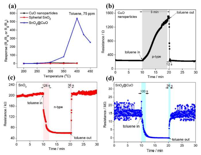
Fig. 5.
(a) The gas sensing response of all samples at different working temperature and response/recovery time of (b) CuO, (c) SnO2 and (d) SnO2@CuO at 400 °C.
To examine the repeatability performance, the CuO decorated-SnO2 based sensor was exposed to different toluene concentrations. Fig. 6(a) displays a transient toluene sensing response of SnO2@CuO to 10-75 ppm toluene gas at its best working temperature (400 °C). It clearly showed that the SnO2@CuO sensor had good remarkable response-recovery property as indicated by recovering of sensor resistance after the ejection of toluene gas even though noise of base resistance was observed.

Fig. 6.
(a) A transient sensing response of SnO2@CuO to different concentrations of toluene gas (b) exponential fitting vs. toluene concentration; y and x-axis represents sensing response and toluene concentration, respectively and R shows quality of fitting, (c) selectivity of SnO2@CuO.
Moreover, the sensor response increased with the increment of toluene gas concentration, as shown in Fig. 6(b). In many cases, the response value had a linear relationship with testing gas concentration using double-logarithmic plot (Y = mX + C, with Y and X were sensing response and concentration, respectively). However, in our study, the sensor response of the SnO2@CuO showed a linear relation with toluene concentration only up to 30 ppm and an exponential improvement of sensing response occurred above 30 ppm which the relationship between response and toluene concentration could be approximately predicted by a exponential function y = exp (-117.25/(x - 10)) where y is sensor response and x is toluene concentration. We pre-suspected that above 30 ppm of toluene gas exposure, the change of physicochemical property of SnO2@CuO sample might be probably occurred which might be caused by phase or surface state alteration. From the standpoint of real implementation, selectivity of sensing material also should be another critical aspect. Thus, gas sensing performance of SnO2@CuO towarded exposure of different reducing gas such as methanol, ethanol and hydrogen was examined. Sensor selectivity is defined as a ratio between response of toluene compared to other gas response (Stoluene/Sothergas). Fig. 6(c) obviously shows the response of SnO2@CuO to 75 ppm of toluene gas is about 5 times higher than during the introduction to ethanol (Stoluene/Sethanol) as compared to n-type SnO2 (1.1) and p-type CuO (2.6), which demonstrates a promise for an excellent and selective toluene gas sensor. The results of the current study were compared to the previous work as listed in Table 1 and it could be seen from the data in Table 1, SnO2@CuO exhibited a comparably high toluene sensing performance, especially for its response and selectivity.
Table 1 Comparison of SnO2-based toluene gas sensing performance.
| Material | T (oC) | Conc. (ppm) | Response (Ra/Rg or Rg/Ra) | Selectivity Rtoluene/Rothergas | Response/ recovery times (s) | Refs. |
|---|---|---|---|---|---|---|
| SnO2-decorated NiO nanostructure | 250 | 100 | 60 | 2 | N/A | [10] |
| NiO -SnO2 composite nanofiber | 330 | 50 | 11 | 3.8 | 11.2 /4 s | [42] |
| SnO2-Fe2O3 Interconnected Nanotubes | 260 | 50 | 25.3 | 7 | 6/10 | [43] |
| Pd-loaded flower-like SnO2 microspheres | 250 | 10 | 17.4 | 1.7 | N/A | [20] |
| Pd- loaded SnO2 cubic nanocages | 230 | 20 | 41.4 | 4.1 | 0.4/16.5 | [18] |
| SnO2-ZnO core-shell nanowires | 300 | 1 | 73 | 2.8 | N/A | [44] |
| CuO-decorated spherical SnO2 | 400 | 75 | 540 | 5 | 100/36 | This work |
After the gas sensing measurement, the samples were recovered from the sensor device and characterized by SEM and XPS to investigate their stability. The SEM images (Fig. S5(a-c)) clearly showed that without CuO loading, the morphology of the spherical SnO2 was damaged. However, after decorating material was loaded, the most of spherical morphology were retained which a significant evidence that the decoration with CuO nanoparticles not only enhanced toluene gas sensing property but also increased thermal stability of the spherical SnO2 base material as it might act as a protective barrier to prevent thermal oxidation. Furthermore, XPS study as displayed in Fig. S6 suggested that surface chemical states (Sn 3d, O 1s and Cu 2p) of SnO2@CuO sample were generally similar with that of fresh sample except for a peak at 932.4 eV attributed to other valence state of Cu which probably Cu (0), indicating good stability of the sensing material even at higher temperature and reducing gas environment.
3.2.2. Effect of amount and particle size of the decorative nanoparticles
We also investigated the effect of the amount of decorative material on toluene sensing response of SnO2@CuO -based sensor. The amount of CuO nanoparticles loaded onto spherical SnO2 was varied from 0.05 to 0.3 mmol. Fig. 7(a) shows the gas sensing response of 0.05, 0.1, 0.2 and 0.3 mmol of CuO loading to 10-50 ppm toluene gas. It was noticed that regardless of the amount of decorating materials, gas sensing response increased as toluene concentration increases. It was also found that the optimum loading amount which exhibited the highest response was 0.1 mmol of CuO. An increase of non p-n junction contact due to an excess amount of p-type CuO had led to the decrement of gas sensing response. In the case of lower amount of CuO, some spherical SnO2 might not be fully decorated by CuO which also reduced sensor response. The relationship between addition of CuO on SnO2@CuO sensor base resistance and their sensor response was further investigated. As presented in Fig. 7(b), without addition of CuO, spherical SnO2 possessed conductive property, as indicated by low resistance during their exposure to ambient air. Addition of 0.05 mmol CuO as decorating particle on spherical SnO2 increased the resistance greatly due to the development of p-n heterojunction and eventually led to increment of sensor response due to the presumably suppressing charge carrier process. Also, we found a good correlation between the sensor resistance and its sensing response i.e., when our sensing material possessed the largest base resistance, it also showed the highest gas sensing response and vice versa. This larger base resistance means more oxygen species adsorbed on the surface of material during the exposure to air and consequently increases more reactions with the target gas leading to higher response [21,22]. Additionally, larger resistance contributed to low concentration of toluene gas. This finding, we believe, is meaningful for the future development of gas sensing materials.

Fig. 7.
(a) Gas sensing response as a function of toluene concentration and (b) relationship between sensor base resistance and toluene sensing response of SnO2@CuO based-sensor with different amount of decorating material.
3.3. Gas sensing mechanism of SnO2@CuO
The toluene gas sensing mechanisms of SnO2@CuO based-sensor should differ from n-type SnO2 based-sensor due to the creation of p-n heterojunction by the decoration with CuO nanoparticles, although SnO2@CuO had shown similar sensing response/recovery charateristics to that n- SnO2. The evidence of p-n heterojunction development at the particle interface had been demonstrated by the HRTEM images as discussed in the earlier section. Moreover, the larger resistance of SnO2@CuO in air (∼15 MΩ) compared to that of pure SnO2 (∼200 kΩ) was another evidence of formation p-n heterojunction [27,29,45]. Therefore, the role of heterojunction structure should be considered for the analysis of sensing mechanism.
The great improvement of gas sensing performance of SnO2@CuO based-sensor might be attributed to the following enhancement factors. (i) Heterostructures of SnO2@CuO with micro-/mesoporosity and large specific surface area could provide better gas diffusion to inner surface of hierarchical structures and more abundant active sites for gas adsorption/desorption reaction during sensing process, respectively. Therefore, they could contribute to faster response/recovery time. (ii) p-n junction formation at the interface between both oxides inhibited charge carrier recombination. In thermal equilibrium, once CuO nanoparticles had attached to the surface of spherical SnO2, electrons in n-type SnO2 would diffuse in reverse direction because of the difference of charge carrier concentration in each oxide, creating an internal electric field at the interface until the balance of carrier concentration is achieved. Consequently, at the depletion layer, energy band bended to develop equal fermi energy level (EF). When the SnO2@CuO-based sensor was exposed to open atmosphere, oxygen molecules were firstly adsorbed on both surface of CuO and SnO2 particles (Eq. (3)). To note, although CuO in TEM images had fully covered SnO2 microsphere, the gas molecules could still be adsorbed on SnO2 surface through the porosity. Then, the adsorbed oxygen was dissociated into ionized-oxygen species (Eq. (4)) by taking charge carrier near the surface of p-type CuO and n-type SnO2 leading to the formation of depletion layer at interface as shown in step (1) of Fig. 8 which increased potential barrier and thus the charge carrier diffusion was blocked. Therefore, compared to pure n-type SnO2 which had only n-n homojunction, the sensor resistance of SnO2@CuO in air was larger due to the thicker depleted-layer and p-n junction potential barrier. During the sensor exposure to toluene gas, the oxygen species was removed from the surface of SnO2@CuO, giving the charge carrier back to respective oxide. This also led to the depleted-layer narrowing which resulted in the decrement of sensor resistance (step (2) of Fig. 8). The whole process would be repeated once the flow of toluene was stopped and air atmosphere was flown.

Fig. 8.
Gas sensing mechanism of CuO nanoparticles-decorated SnO2 microsphere. EDLs = Electron Depletion Layers. HALs = Hole Accumulation Layers.
However, as we observed in Fig. 6(b) that the sensor response was not linear with toluene concentration, especially above 40 ppm. Thus, we proposed more detail sensing mechanism to explain this phenomenon. In the case of high toluene concentration (∼40 ppm), i.e., when all oxygen ions species were removed in step 2, the process proceeded to the partial reduction of CuO nanoparticles to form Cu metal by excess toluene gas (Eq. (6)), destroying the p-n heterocontact and charge depletion layer. This process would create another heterocontact between metallic Cu nanoparticles and n-type SnO2 (step 3) so-called by ohmic-contact (non-rectifying contact) where this type of heterocontact possessed very low resistance junction. The same phenomenon was also found in H2S exposing environment [46,47]. The SnO2 band bent downward due to the work function of the metallic phase Cu was lower than that of SnO2 [48,49]. As a result, the sensor resistance would further decrease. In the final step, the flow of air at high temperatures caused oxidation of Cu metal to CuO nanoparticles and the depletion region at the interface was rebuilt at the latter process (step 4).
The existence of Cu metal was confirmed by the XPS study. The sample for XPS characterization was taken after the gas sensing test. However, after exposing the sensor device to 75 ppm of toluene gas for 10 min, instead of ambient airflow, pure nitrogen was used to remove toluene gas until the measurement system cooled down to room temperature in order to prevent oxidation. As displayed in Fig. 9(a), the XPS confirmed the presence of Sn, O and Cu elements. Specifically, as seen in Fig. 9(b), Cu 2p core-level spectra (Cu 2p1/2 and Cu 2p3/2) was slightly shifted to lower binding energy than that of the fresh sample in Fig. 3(d) which might be contributed by Cu metal (Cu (0)) since the peak of Cu metal located at lower binding energy (932.4 and 952.2 eV) than Cu with the oxidation state of +2 in CuO (935.7 eV). Our XPS study result was very close to the past study [50]. They suggested that Cu (0) binding energy was located at 932.6 eV which had a similar value in case of our recent study. Additionally, disappearance of satellite peaks (∼942 eV and ∼962 eV) further confirmed the presence of Cu metal, although the binding energy at 935.7 eV confirmed a small fraction of CuO phase. These facts strongly suggested the partial formation of Cu metal during the exposure of high concentration of toluene. The partial reduction of CuO might become a reason for why pure CuO still exhibiting p-type property, where the resistance increased under the high ppm of toluene gas.

Fig. 9.
(a) Full spectra and (b) Cu 2p core spectra of SnO2@CuO after exposure to 75 ppm of toluene gas and cooled down in nitrogen atmosphere.
The sensor device containing SnO2@CuO sample was re-evaluated to investigate the thermal stability since we found a small fraction of Cu (0) phase might still present. The gas sensing reevaluation was performed at 400 °C under exposure of 75 ppm of toluene gas. As shown in Fig. S7, the sensor device still showed a transient response/recovery curve similar to the first investigation. However, a slight change in the base resistance of sensor device as well as its responsivity (S = 604) could be observed. The existence of Cu (0) in the SnO2@CuO sample might induce the ohmic contact and thus altering the base sensor resistance and toluene sensing response. Lastly, we performed toluene gas sensing response of SnO2@CuO under different relative humidity (RH) and as shown in Fig. S8, it could be found that the response of SnO2@CuO samples decreased as RH increased which was probably attributed to the competition between water vapor and toluene gas to react with the adsorbed oxygen ion [14,39,51].
4. Conclusions
In conclusion, CuO nanoparticles and spherical SnO2 with high specific surface area (over 90 m2/g) was successfully synthesized by non-hydrolytic approach. Using a facile decoration process, we were able to decorate spherical SnO2 with CuO nanoparticles with good uniformity which caused by electrostatic interaction. Owing to (i) p-n heterojunction structure in combination with a high specific surface area and porous property, CuO nanoparticles decorated-spherical SnO2 showed a significant improvement to toluene gas sensing responsivity (Ra/Rg = 540, 75 ppm) as well as excellent gas selectivity. Moreover, (ii) the formation of Cu metal during the exposure of high concentration toluene which destroying p-n junction and created ohmic contact with n-type further improved the gas sensing properties. The SnO2@CuO based sensor also demonstrated very high chemical and morphological stability at harsh environment that might meet the requirement for high temperature toluene gas sensor applications.
Reference

 WeChat