Search for articles:
Song Jiang , Hui-Ming Cheng
Corresponding authors:
Received: 2019-03-7
Revised: 2019-04-24
Accepted: 2019-06-12
Online: 2019-11-05
Copyright: 2019 Editorial board of Journal of Materials Science & Technology Copyright reserved, Editorial board of Journal of Materials Science & Technology
More
Abstract
A single-wall carbon nanotube (SWCNT) has superior optical, electrical, and mechanical properties due to its unique structure and is therefore expected to be able to form flexible high-performance transparent conductive films (TCFs). However, the optoelectronic performance of these films needs to be improved to meet the requirements of many devices. The electrical resistivity of SWCNT TCFs is mainly determined by the intrinsic resistivity of individual SWCNTs and their junction resistance in networks. We analyze these key factors and focus on the optimization of SWCNTs and their networks, which include the diameter, length, crystallinity and electrical type of the SWCNTs, and the bundle size and interconnects in networks, as well as chemical doping and microgrid design. We conclude that isolated/small-bundle, heavily doped metallic or semiconducting SWCNTs with a large diameter, long length and high crystallinity are necessary to fabricate high-performance SWCNT TCFs. A simple, controllable way to construct macroscopic SWCNT networks with Y-type connections, welded junctions or microgrid design is important in achieving a low resistivity. Finally, some insights into the key challenges in the manufacture and use of SWCNT TCFs and their prospects are presented, hoping to shed light on promoting the practical application of SWCNT TCFs in future flexible and stretchable optoelectronics.
Keywords:
Transparent conductive films (TCFs) are thin films that are optically transparent and electrically conductive. They are an important component in many optoelectronic devices including touch screens, liquid crystal displays (LCDs), organic light-emitting diodes (OLEDs), and photovoltaics (PVs), all of which have different performance requirements [[1], [2], [3]] (Table 1). Indium tin oxide (ITO) is currently the most widely used commercial TCF material because of its superior optoelectronic performance. The sheet resistance (Rs) of an ITO TCF reaches ∼10 Ω/sq. (ohms per square) at 90% transmittance (T) for 550-nm light [[3], [4], [5]]. However, the limited reserves of indium and the brittleness of ITO are drawbacks for its use in flexible and stretchable optoelectronics that has developed rapidly in recent years. Alternative transparent conductive materials with good flexibility have been intensively investigated, such as carbon nanotubes (CNTs) [[6], [7], [8], [9]], graphene [10], metal nanowires [11], metal meshes [12], conducting polymers [13], and various hybrids [[14], [15], [16]]. Among them, CNTs are considered a very promising candidate because of their unique structure which gives them excellent flexibility, low intrinsic electrical resistivity, high structural stability, and the desired optical properties of a wide spectral transmittance range, low refractive index, little coloration, and low haze, especially when composed of single-wall carbon nanotubes (SWCNTs) [2,3,[17], [18], [19]]. Therefore, CNT-based TCFs have attracted considerable research interest in recent years because of their wide-range of potential applications [[20], [21], [22], [23]].
Table 1 Performance requirements for the practical applications of TCFs [
| Application | Minimum T (%) | Maximum Rs (Ω/sq.) |
|---|---|---|
| Touch screens | 85 | 500 |
| LCDs | 85 | 100 |
| OLEDs | 90 | 50 |
| PVs | 90 | 10 |
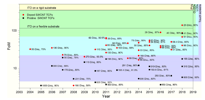
In 2004, Rinzler et al. [6] first fabricated a SWCNT TCF by a vacuum filtering method. It showed a Rs of 30 Ω/sq. at over 70% T in the visible spectral range. The methods of fabricating SWCNT TCFs can be classified into wet processes (including vacuum filtering) and dry processes. A detailed introduction to the fabrication of the films will be given in the next section. Table 2 [[6], [7], [8], [9],[24], [25], [26], [27], [28], [29], [30], [31], [32], [33], [34], [35], [36], [37], [38], [39], [40], [41], [42], [43], [44], [45], [46], [47], [48], [49], [50], [51], [52], [53], [54]] shows the optoelectronic performance of typical films reported since 2004 that have been fabricated by these two methods. It can be seen that the performance of those films fabricated by dry processes is much higher. However, most pristine films had Rs values of over 150 Ω/sq. at 90% T for 550-nm light (FoM = 23.2), which are much higher than the values for ITO on rigid and flexible substrates which are respectively ∼10 Ω/sq. (FoM = 348.5) [5] and ∼30 Ω/sq. (FoM = 116.2) [55]. Chemical doping is effective in lowering the Rs of the films, however, the performance is usually unstable and cannot compete with ITO TCFs. We summarize the representative optoelectronic performance of SWCNT TCFs reported since 2004 in Fig. 1, from which it can be seen that their performance has gradually improved. However, the performance of most pristine and doped films can only meet the requirements of low-end TCFs for use in touch screens and LCDs, and is far from the requirements of high-end OLEDs and PVs. Further investigations on the optimization of the structure and performance of SWCNT TCFs are therefore important.
Table 2 Representative SWCNT TCFs fabricated by wet and dry processes.
| Year | Preparation method | Rs (pristine) (Ω/sq.) | Dopant | Rs (doped) (Ω/sq.) | T (%) | FoM (pristine) | FoM (doped) | Ref. |
|---|---|---|---|---|---|---|---|---|
| 2004 | Wet process | HNO3 | 30 | 70 | 32.2 | [6] | ||
| 2005 | Wet process | 1000 | 90 | 3.5 | [24] | |||
| 2006 | Wet process | 300 | NO2 | 100 | 90 | 11.6 | 34.8 | [25] |
| 2007 | Wet process | 175 | HNO3 | 70 | 80 | 9.1 | 22.8 | [26] |
| 2007 | Dry process | 50 | 70 | 19.3 | [27] | |||
| 2008 | Wet process | 1560 | SOCl2 | 180 | 59 | 0.4 | 3.5 | [28] |
| 2008 | Wet process | 231 | 75 | 5.3 | [29] | |||
| 2009 | Wet process | 110 | 80 | 14.5 | [30] | |||
| 2009 | Wet process | HNO3+ H2SO4 or HCl | 270 | 93.5 | 20.4 | [31] | ||
| 2010 | Wet process | 187 | 80 | 8.5 | [33] | |||
| 2010 | Dry process | 820 | HNO3 | 110 | 90 | 4.2 | 31.7 | [32] |
| 2011 | Wet process | CSA | 60 | 90.9 | 64.3 | [7] | ||
| 2011 | Wet process | 600 | AuCl3 | 36 | 85 | 3.7 | 61.9 | [35] |
| 2011 | Wet process | HNO3+ H2SO4 | 133 | 90 | 26.2 | [36] | ||
| 2011 | Wet process | 198 | AuCl3 | 85 | 90 | 17.6 | 41.0 | [34] |
| 2012 | Wet process | 198.4 | 81.8 | 9.0 | [38] | |||
| 2012 | Wet process | H2SO4 | 100 | 90 | 34.8 | [37] | ||
| 2013 | Wet process | HNO3+ SOCl2 | 86 | 80 | 18.6 | [39] | ||
| 2013 | Wet process | HNO3 | 68 | 89 | 46.2 | [40] | ||
| 2014 | Dry process | HNO3 | 160 | 90 | 21.8 | [42] | ||
| 2014 | Dry process | 95 | 80 | 16.8 | [41] | |||
| 2014 | Dry process (patterning) | 300 | HNO3 | 53 | 80 | 5.3 | 30.1 | [41] |
| 2014 | Dry process | 291 | AuCl3 | 73 | 90 | 12.0 | 47.7 | [54] |
| 2015 | Dry process | HNO3 | 63 | 90 | 55.3 | [8] | ||
| 2015 | Wet process | 183.6 | HNO3 | 34 | 81 | 9.2 | 49.9 | [44] |
| 2015 | Wet process | CuI | 55 | 85 | 40.5 | [45] | ||
| 2015 | Dry process | 310 | 90 | 11.2 | [43] | |||
| 2016 | Dry process | 950 | HNO3 | 89 | 90 | 3.7 | 39.2 | [46] |
| 2016 | Dry process (patterning) | HNO3 | 29 | 87 | 90.1 | [46] | ||
| 2016 | Dry process | CuCl | 98 | 90 | 35.6 | [47] | ||
| 2017 | Dry process | CuCl2/ Cu(OH)2 | 69.4 | 90 | 50.2 | [48] | ||
| 2017 | Dry process | 250 | HNO3 | 51 | 80 | 6.4 | 31.3 | [49] |
| 2018 | Wet process | 310 | 90 | 11.2 | [51] | |||
| 2018 | Dry process | 41 | HNO3 | 25 | 90 | 85.0 | 139.4 | [9] |
| 2018 | Dry process | AuCl3 | 86 | 90 | 40.5 | [52] | ||
| 2018 | Dry process | 195 | HNO3 | 51 | 90 | 17.9 | 68.3 | [50] |
| 2018 | Dry process | 600 | HAuCl4 | 40 | 90 | 5.8 | 87.1 | [53] |
Fig. 1. Representative SWCNT TCF performance since 2004 together with those of ITO TCFs on rigid and flexible substrates, as well as the performance requirements for practical applications in touch screens, LCDs, OLEDs, and PVs.
In this review, we first introduce the methods of fabricating SWCNT TCFs and the working mechanisms. This is followed by a review of recent research progress on fabricating films with an improved optoelectronic performance and finally we discuss the developing trends and remaining key challenges for their use in flexible and stretchable optoelectronics.
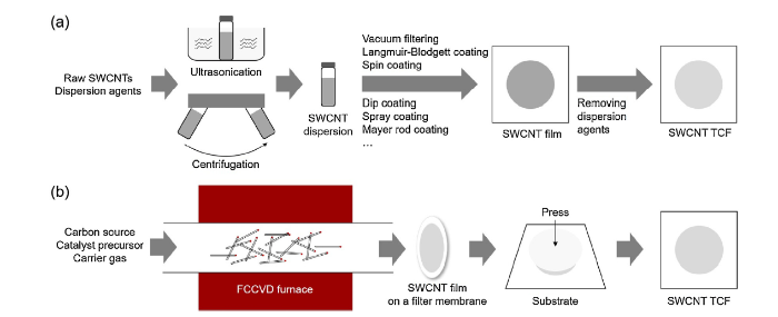
Fig. 2(a) shows details of the fabrication of SWCNT TCFs by a wet process. Raw SWCNTs are usually first dispersed by ultrasonication in a solution with the help of dispersion agents. This is followed by centrifugation which leaves an upper layer of monodispersed SWCNTs without catalysts and big bundles which is decanted to be used to fabricate the films. In recent years, many wet methods including vacuum filtering [6], spin coating [57], Langmuir-Blodgett coating [58], dip coating [59], spray coating [60], and Mayer rod coating [61] have been developed for the fabrication of SWCNT TCFs. An obvious drawback of wet process is that the dispersion of SWCNTs and chemical treatment usually introduce defects in the tubes. It is also difficult to completely remove the dispersion agents from the surface of the SWCNTs, and these degrade the optoelectronic performance of the resulting films. Therefore, many factors including the source of the SWCNTs, the degree of monodispersion, solution stability, coating and drying parameters, and the efficiency of removal of the dispersion agents influence the performance of films prepared by a wet process. These drawbacks can be avoided using a dry process Kauppinen et al. [32] first reported a SWCNT TCF prepared by dry gas filtration, and the details are shown in Fig. 2(b). First, SWCNTs are synthesized by a floating catalyst chemical vapor deposition (FCCVD) method [62]. These floating as-grown SWCNTs are carried by the gas flow to a porous filter membrane at the outlet of CVD furnace where they self-assemble into a film. The thickness of the film is determined by the collection time. It can be transferred to another substrate by simply pressing the filter membrane onto it. The process involves no liquid and the intrinsic properties of the SWCNTs are well preserved. As a result, a dry process has obvious advantages over wet processes in fabricating high-performance SWCNT TCFs. This review mainly focuses on the improvement of the optoelectronic performance of these films by controlling their structure. Some previous reviews [2,18,19] can be referred to for more details about the fabrication.
Fig. 2. Schematic showing the fabrication of SWCNT TCFs by (a) a wet process and (b) a dry process.
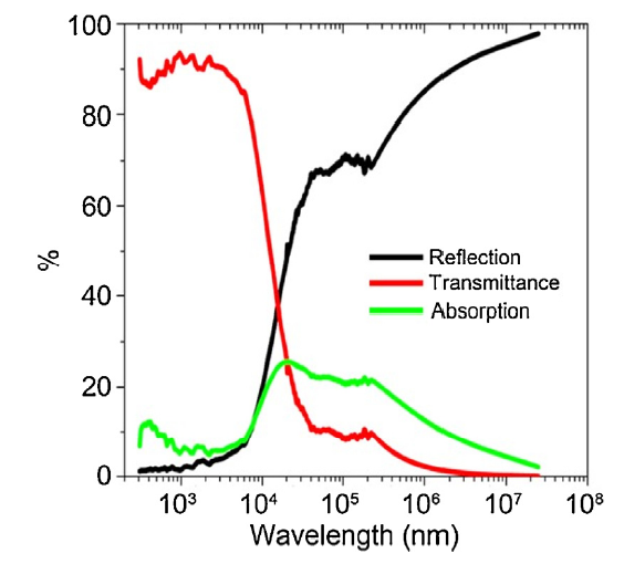
T is a primary performance metric of TCFs. When incident light passes through an object, some will be reflected, some absorbed and some transmitted. For SWCNT TCFs, the reflection and absorption of light are mainly determined by the interaction between light and free carriers. The plasma wavelength (λp) is an important index of light reflection, and indicates that incident light will be mostly reflected by the film if its wavelength is longer than λp. Classical Drude theory shows λp ∝ n-1/2 where n is the carrier concentration, from which we can see that λp increases with a decrease of n. At room temperature, SWCNTs have an n value of the order of 1017 cm-3, which is much lower than those of metals (∼1022 cm-3), ITO (∼1021 cm-3) and graphene (∼1020 cm-3) [3,63]. The corresponding λp of the nanotubes is >10 μm, which means that its reflection is very low when the light wavelength is <10 μm. By contrast, the λp values of metals, ITO, and graphene are ∼200 nm, ∼800 nm, and several microns, respectively. Therefore, SWCNTs have an obvious advantage over other TCF materials for this optical property, especially in the near-infrared and middle-infrared spectral ranges. Light absorption of SWCNT TCFs results from electron transitions from valence band to conduction band. SWCNTs with different chiralities absorb light of different energies, and the main absorption peaks are in the visible and near-infrared spectral range. Because of the low value of n, electron transitions are limited, which suppresses light absorption. Another important feature of a SWCNT network is its open areas that are not covered by SWCNTs. These areas help light transmission which is different from normal ITO and graphene TCFs. Therefore, SWCNT TCFs have an excellent T for wavelengths shorter than λp (Fig. 3) [63]. Some of T is forward scattered light, known as haze, and this is undesirable for display applications. Because of their nanoscale diameter and low n value, SWCNTs produce very little haze (<1%) [17,64] and therefore have excellent optical properties for TCF applications.
Fig. 3. Calculated reflection, transmittance, and absorption of a SWCNT TCF in the broad spectral range from 400 nm to 2 cm [
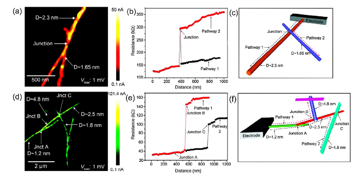
Rs is another primary performance metric of TCFs. Because the value of n for SWCNTs is as low as ∼1017 cm-3 [63] and the intrinsic carrier mobility is as high as 105 cm2/(V s) [65] at room temperature, SWCNT TCFs are expected to have a very low Rs at a specific T. However, the highest measured carrier mobility of a SWCNT network is only 1027 cm2/(V s) [66], which indicates that some important factors limit the performance of SWCNT networks. When a voltage is applied to a SWCNT network, free carriers inside a tube will move along the wall and hop or tunnel into the second tube at junctions. Thus, the Rs of the whole network can be divided into two parts: the intrinsic resistance of SWCNTs and the resistance of intertube junctions. Many studies [56,[67], [68], [69]] have showed that the resistance of intertube junctions dominates the Rs value of a SWCNT network. Boland et al. [67] investigated the electrical resistance of sparse SWCNT networks by conductive atomic force microscopy, and found that the junction resistance was much higher than the intrinsic resistance (Fig. 4). This is attributed to two factors. First, intertube contacts in the network are mostly point-contact, and the local intertube structure of SWCNTs is somewhat similar to the layer structure of graphite. It is well-known that the resistivity of graphite along the c-axis is much higher than in plane [70]. Second, almost all the junctions are heterojunctions because different SWCNTs have different chiralities and diameters, which means that they can be of different electrical types and have different band gaps. As a consequence, the junction resistance is much higher than the intrinsic resistance of the SWCNTs, especially for junctions between metallic (m-) SWCNTs and semiconducting (s-) SWCNTs, which are Schottky contacts (not ohmic contacts). Such contacts are common because of p-doping by ambient oxygen (O2) when the films are exposed to air [[71], [72], [73]]. By contrast, the contacts between tubes of the same type are (near-) ohmic. The junction resistance between m- and s-SWCNTs is as large as 100-20,000 kΩ, much higher than those at junctions between similar types (20-400 kΩ) [71,74]. In addition, these junction resistances are much higher than the intrinsic resistance of SWCNTs of 6-20 kΩ/μm [67,75]. Furthermore, SWCNTs synthesized by conventional methods are usually a mixture of ∼1/3 m- and ∼2/3 s-SWCNTs so that ∼4/9 of intertube junctions are Schottky contacts, which greatly increase Rs. Actually, the number of contacts along carrier paths will be reduced if the lengths of the SWCNTs are increased, so that the growth of longer SWCNTs is another way to reduce the electrical resistivity of SWCNT networks.
Fig. 4. Conductive atomic force microscopy results on pristine sparse SWCNT networks. (a) Current map of a bundle ∼2.3-nm diameter, which overlaps an individual tube of ∼1.65-nm diameter. The electrode is positioned on the top of the image (not shown). (b) Local resistance analysis through a bundle and an individual tube depicted as pathways 1 and 2 in the schematic (c). (d) Current map of interconnected tubes of different diameters showing the formation of junctions with different resistances. (e) Local resistance analyzed along an individual tube connected to a sparse configuration of nanotubes highlighted as pathways 1 and 2 in the schematic (f). The electrode is positioned on the left side of the image (not shown) [
Because of their small size and the strong van der Waals interactions between them, SWCNTs usually aggregate into bundles with diameters of several to tens of nanometers or even larger. These bundles generally decrease the optoelectronic performance of the films. On one hand, the SWCNTs in a bundle are densely packed, and the radial resistivity is much higher than the axial resistivity [70]. In consequence, the carrier transport between different tubes is severely suppressed, which results in high junction resistance between the tubes in a bundle and interbundles (Fig. 4) [67]. On the other hand, carrier transport mainly occurs along the outermost layer of a bundle, leaving the bundle core as “dead mass” that only contributes to optical absorption [76]. Thus, bundling of SWCNTs leads to a higher Rs and a lower T. For the tube itself, defects in the tube formed during synthesis or post-treatment reduce the mean free paths of carriers and decrease carrier mobility. They therefore can be a serious factor that increases the electrical resistivity of SWCNT networks. Finally, SWCNTs with large diameters have smaller bandgaps, much high carrier concentrations [77,78], and larger contact areas at intertube junctions, which can reduce the intrinsic tube resistance and the junction resistance. Therefore, films composed of SWCNTs with large diameters are more electrically conductive. The above discussion indicates that the electrical resistivity of SWCNT networks is determined by many factors including the junction resistance, bundle size, and SWCNT quality (crystallinity), diameter, electrical type and length. In the following section, we will elucidate the progress in improving the performance of SWCNT TCFs by controlling the SWCNT structure and the configuration of the networks.
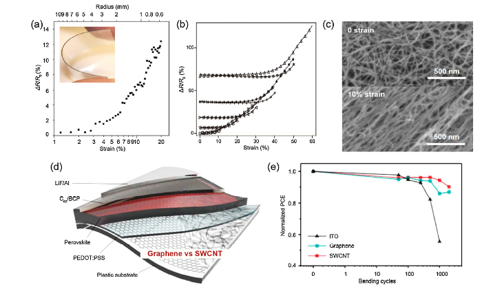
For flexible electronics, the flexibility of SWCNT TCFs is an important metric. SWCNTs are intrinsically flexible and elastic because of their large aspect ratio and strong atomic bonding [79,80]. When flexible SWCNTs are assembled into a thin film on a flexible polymer substrate, the low-frictional forces between tubes and bundles [81,82], the large % void volume [19], and the strong molecular coupling between polymer molecules and SWCNTs [83] give the film excellent flexibility, stretchability, and even foldability. Fig. 5(a) [84] shows the electrical resistance (R) change of a SWCNT TCF on a polystyrene substrate fabricated by a wet process under different bending radii (strains). We see that the film shows less than a 10% change in R when bent to a radius of curvature of 1 mm (∼10% strain), which satisfies the demands of commercial TCFs and is far better than an ITO TCF on a flexible substrate. Fig. 5(b) [83] shows the R change of a SWCNT TCF fabricated by a dry process on a poly(dimethylsiloxane) substrate when it was subjected to repeated stretch and release cycles. At the first loading stage (10% strain), R increased by 5%, which is similar to that of the film fabricated by a wet process shown in Fig. 5(a). When the strain was released, the R change decreased and remained almost constant (about 1%). This reversible phenomenon was attributed to the elastic elongation of the SWCNTs and interbundle junctions. In addition, the film did not crack until loaded to a 60% strain (critical strain), which is much higher than a free-standing SWCNT TCF [27]. Therefore, the strong interaction between the flexible polymer substrate and the SWCNTs can increase the critical strain of the film and enhance its flexibility. Fig. 5(c) [83] shows scanning electron microscopy (SEM) images of a SWCNT TCF under different strains. It can be seen that a tensile strain of 10% aligns the SWCNTs in the tensile direction, which is mainly accommodated by the SWCNT elastic elongation and sliding between bundles. Maruyama et al. [49] used SWCNT and graphene TCFs on plastic substrates as the anodes of inverted perovskite solar cells (Fig. 5d) and tested their mechanical reliability. They found that after 1000 bending cycles the performance of the SWCNT-based cell decreased by only ∼5%, which means that the film has excellent cyclic bending performance. In contrast, the performance of graphene and ITO-based cells decreased by ∼15% and ∼45%, respectively (Fig. 5(e)). Therefore, SWCNT TCFs have excellent mechanical properties in terms of good flexibility and stability during deformation.
Fig. 5. Mechanical properties of SWCNT TCFs. (a) Change of R for a SWCNT TCF on a polystyrene substrate fabricated by a wet process under different bending radii (strains). Inset is an optical image of the SWCNT TCF [
In recent years, many strategies including control of the structure of the SWCNTs, optimizing of the network configuration, chemical doping and patterning (microgrid design) have been developed to improve the performance of SWCNT TCFs.
The diameter, length, defect content, and electrical type will greatly influence the optoelectronic performance of SWCNT TCFs.
4.1.1. Diameter, length and quality
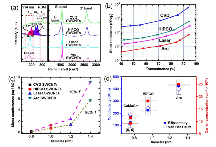
As discussed earlier, large-diameter and long SWCNTs with high quality are preferable for constructing high-performance TCFs. Young et al. [85] have studied the effects of diameter and quality on the optoelectronic performance of SWCNT TCFs. They compared the structures of four SWCNT samples and their TCF performance. As shown in Fig. 6(a), the diameters [86] and the intensity ratios of the G and D bands (IG/ID values, higher IG/ID value means better crystallinity [87]) of the four SWCNT samples are quite different, which will result in distinctly different TCF performance. As shown in Fig. 6(b), the optoelectronic performance of Arc SWCNT and Laser SWCNT TCFs is much better than those of high-pressure carbon monoxide (HiPCO) SWCNT and CVD SWCNT TCFs. The larger diameters of Arc SWCNTs and Laser SWCNTs lead to lower intrinsic and junction resistances and their higher IG/ID values (Fig. 6(a)) indicate their higher crystallinity. Therefore, the larger diameters and fewer defects of Arc and Laser SWCNTs account for their better TCF performance (Fig. 6(b) and (c)). The best result achieved for pristine Arc SWCNT TCFs is ∼390 Ω/sq. at 90% T (FoM = 8.9) for 550-nm light. The advantage of the large-diameter Arc SWCNTs has been also verified by Battie et al. [78] who found that the electrical conductivity of Arc, HiPCO and CoMoCat SWCNTs decreased with the decreasing diameter and carrier (hole) concentration which were characterized by ellipsometry and theoretical simulations (Fig. 6(d)).
Fig. 6. Optical and electrical characterization of CVD, HiPCO, Laser, Arc, and CoMoCat SWCNT samples. (a) Raman spectra (the tube diameters calculated from corresponding radial breathing mode (RBM) peaks are 1.43 nm, 1.35 nm, 1.25 nm, 0.96 nm, and 0.79 nm, respectively) and (b-d) optoelectronic performance [
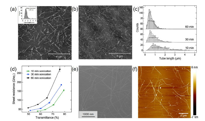
Several studies have been dedicated to understanding the effect of tube length (not bundle length) on SWCNT TCF performance [60,88,89]. Blackburn et al. [60] adopted a new surfactant of sodium carboxymethyl cellulose (CMC) to disperse high-quality Laser SWCNTs [90]. This dispersant [91] is very effective in obtaining a monodispersed and stable SWCNT dispersion. By controlling the dispersion sonication time in the range 10 to 60 min, the mean length of the tubes can be changed from 1.32 μm to 0.55 μm (Fig. 7(a-c)). Atomic force microscopy (AFM) observations indicated that the average diameter of the tubes was ~1.3 nm (Fig. 7(a)). They then fabricated TCFs using a spraying method. Fig. 7(d) shows the performance of SWCNT TCFs with different lengths, from which it can be seen that the 1.32-μm-length film has a ∼2.5 times lower Rs than the 0.55-μm-length film at the same T. Interestingly, the ~2.5 times decrease in Rs is almost the same as the 2.4 times increase in tube length. This suggests that Rs may decrease linearly with increasing tube length over a certain range, which has been proven by Ferreira and Kauppinen et al. [43,92]. Wang et al. [89] also obtained TCFs from monodispersed long SWCNTs. The tube lengths are in the range of 10-25 μm (Fig. 7(e) and (f)), much longer than those reported in other studies (several hundred nanometers to several micrometers) [8,60,88]. Transmission electron microscopy (TEM) observations indicated that the average diameter of the tubes was ~2.4 nm. However, the performance of TCFs based on these large-diameter, long SWCNTs was not as high as expected, and they showed a Rs of 286 Ω/sq. at 92% T (FoM = 15.5) for 550-nm light after HNO3 doping. This may be caused by a residue of the insulating dispersant and the low quality of the SWNCTs with an IG/ID value of $\widetilde{1}$0. The dispersion agent residue causes a higher junction resistance between tubes and a higher Rs. The low IG/ID value suggests that there is a high concentration of defects in the tubes, which scatters carriers and increases the Rs.
Fig. 7. AFM images of CMC-dispersed SWCNTs on a silicon wafer made by (a) 10-minute sonication and (b) 60-minute sonication. (c) Length distribution measured by AFM. (d) Optoelectronic performance of CMC-dispersed SWCNTs [
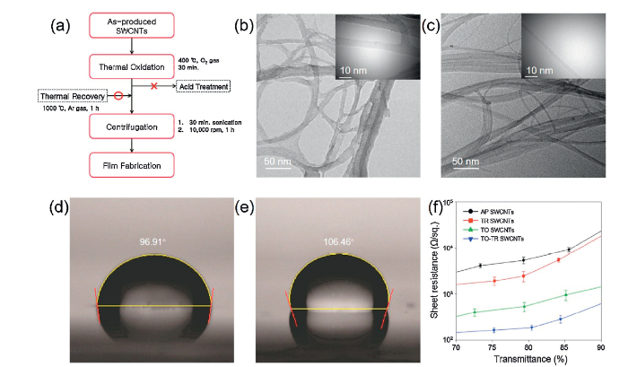
A fast and efficient technique has been developed to purify SWCNTs and to heal tube defects [33] (Fig. 8(a)). Instead of purifying and doping as-prepared SWCNTs by an acid treatment, Han et al. [33] used thermal oxidation (TO) and thermal recovery (TR) to obtain stable, high-performance SWCNT TCFs. The TO removes amorphous carbon surrounding the Arc SWCNTs, and TR in Ar at 1000 °C heals the defects in the tubes (Fig. 8(b) and (c)). TR also eliminates functional groups on the tubes, which was proven by the different contact angles of the samples (Fig. 8(d) and (e)). Fig. 8(f) shows that the TO-TR film has a ~3 times lower Rs than the TO film at the same T. For example, the Rs of the former is 187 Ω/sq. at 80% T (FoM = 8.5) for 550-nm light, whereas the corresponding value of the latter is 540 Ω/sq. at 80% T (FoM = 3.0). Therefore, the TO-TR process is effective in improving the performance of SWCNT TCFs. Some studies [87,93] showed that commercial Laser SWCNTs have a higher quality than commercial Arc SWCNTs, therefore, Laser SWCNTs produced TCFs with the best performance [93]. However, Saito and Kataura et al. [87,94] demonstrated that SWCNTs synthesized by a direct injection pyrolytic synthesis (DIPS) FCCVD method had the highest quality and purity, along with a large diameter. Therefore, SWCNTs synthesized by this method may be the most promising for the fabrication of high-performance SWCNT TCFs.
Fig. 8. SWCNT film fabrication and characterization of TO and TO-TR samples. (a) Schematic of SWCNT film fabrication. TEM images of (b) TO and (c) TO-TR samples. Contact angle tests with water droplets for (d) TO and (e) TO-TR samples. (f) Optoelectronic performance of different samples [
4.1.2. Electrical type
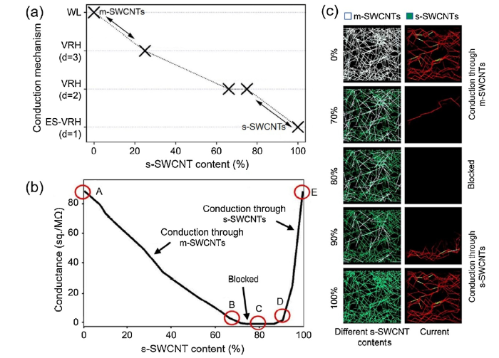
SWCNTs can be either metallic or semiconducting, depending on their chirality. m- and s-SWCNTs show different optoelectronic properties due to their difference in band gap, carrier concentration and doping behavior [78]. Theoretical calculations indicate that the intrinsic resistance of an s-SWCNT is ∼104 times higher than that of an m-SWCNT with the same diameter and length at room temperature [95]. If the semiconducting tube is doped, its conductivity may reach the same order of magnitude as the metallic tube due to the rapid increase of carrier concentration [78,96]. However, normal SWCNT samples are usually comprised of ∼1/3 m- and ∼2/3 s-SWCNTs, which makes it difficult to study the effect of SWCNT electrical type on their TCF performance. Yanagi et al. [97] used a modified density gradient ultracentrifugation (DGU) technique to obtain SWCNTs with different m- to s-SWCNT ratios to study transport mechanisms in mixed SWCNT networks (Fig. 9(a)). When the content of m-SWCNTs was small, Coulomb interactions between electrons of distant m-SWCNTs induced a soft Coulomb gap in the density of states of conduction. Therefore, Efros & Shklovskii-variable range hopping (ES-VRH) conduction occurs. However, when the m-SWCNT content was increased, it increased the screening of the Coulomb potential, resulting in a weakening of Coulomb interactions, and the conduction mechanism changed from ES-VRH to conventional VRH. For a pure m-SWCNT network, boundaries between tubes or bundles acted as weak sources of disorder. As a result, quantum transport was achieved in such a macroscopic network and its conduction mechanism was weak localization (WL). Therefore, different m- to s-SWCNT ratios result in different conduction mechanisms (Fig. 9(a)). Goldhaber-Gordon et al. [96] also studied the electrical transport of thin SWCNT networks with different m- to s-SWCNT ratios by theoretical calculations (Fig. 9(b) and (c)). They found that pure m- or s-SWCNT networks (ambient O2 p-doped) had the highest conductance because of the absence of Schottky barriers between m- and s-SWCNTs. In contrast, the conductance of a normal network with ∼2/3 s-SWCNTs was almost the lowest because the carrier transport in the network was blocked by a large number of Schottky barriers. Therefore, TCFs composed of pure m- or s-SWCNTs are expected to have a much better optoelectronic performance.
Fig. 9. Conduction of SWCNT networks containing a mixture of m- and s- SWCNTs with different s-SWCNT contents. (a) Conduction mechanism in SWCNT networks versus s-SWCNT content as evaluated from absorption spectra [
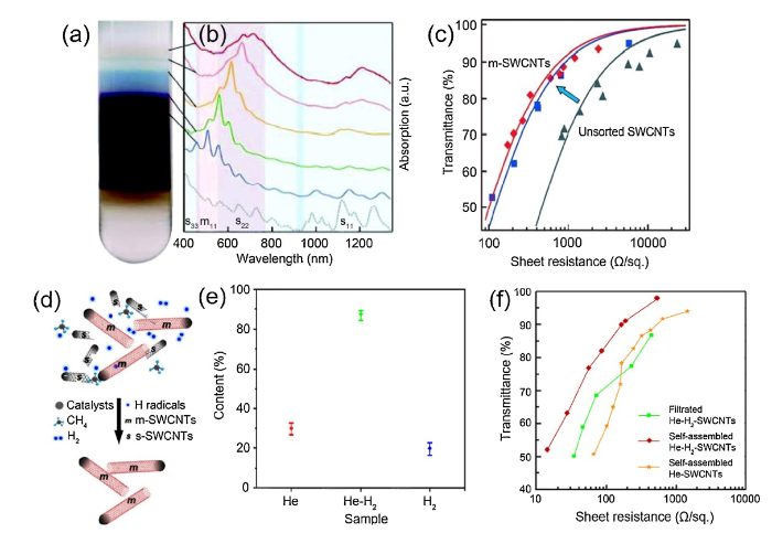
Hersam et al. [29] studied the performance of SWCNT TCFs experimentally enriched with m-type tubes. Double surfactants of sodium dodecyl sulfate (SDS) and sodium cholate were used to obtain monodispersed HiPCO SWCNTs with diameters in the range 0.7-1.3 nm, and DGU was used to separate m-SWCNTs from s-SWCNTs (Fig. 10(a)). Absorption spectra (Fig. 10(b)) show that an upper-middle layer was enriched with m-SWCNTs, even though some s-SWCNTs were present. Fig. 10(c) shows that the TCF enriched with m-SWCNTs exhibits a ∼6 times lower Rs than an unsorted SWCNT TCF at the same T for the visible spectral range. For 1600-nm light in the near-infrared, the performance of TCF enriched with m-SWCNTs was further increased to 10 times. This phenomenon results from the first transition energy of s-SWCNTs which corresponds to the near-infrared range. In the m-SWCNT enriched sample the semiconducting component is greatly decreased which gives a higher T and a higher FoM for the near-infrared range. Our group [42] reported a TCF enriched with m-SWCNTs synthesized by an in-situ etching FCCVD method (Fig. 10(d) and (e)). These SWCNTs were deposited and self-assembled into a thin film on the surface of an aluminum foil, then, press-transferred onto a transparent substrate. The TCFs showed a Rs of ∼650 Ω/sq. at 90% T (FoM = 5.4) for 550-nm light. The FoM value is close to that of the TCFs formed using monodispersed HiPCO SWCNTs enriched with m-type tubes [29]. Actually, the FCCVD SWCNTs should have much longer lengths and larger diameters than the HiPCO ones but their similar FoM values are likely the result of the bundling of the FCCVD SWCNTs. After HNO3 doping, the Rs of the FCCVD films decreased to 160 Ω/sq. at 90% T (FoM = 21.8) for 550-nm light. Blackburn and Kim et al. [28,98] constructed high-performance SWCNT TCFs enriched with s-type tubes and found that HNO3-doped films showed excellent performance with a Rs of 59 Ω/sq. at 80% T (FoM = 27.1) for 550-nm light. These results indicate that isolated and doped m- or s-SWCNTs are excellent for constructing high-performance TCFs. However, a big challenge remains to prepare high-purity, long, and isolated m- or s-SWCNTs with few structural defects.
Fig. 10. Preparation and optoelectronic performance of SWCNT TCFs enriched with m-SWCNTs. (a) Picture of the monodispersed SWCNT solution and (b) corresponding absorption spectra. (c) Performance of metallic and unsorted SWCNTs [
Apart from individual SWCNTs, optimizing the configuration of SWCNT networks including the bundle size and the structure of junctions is equally important for improving their optoelectronic performance.
4.2.1. Bundle size
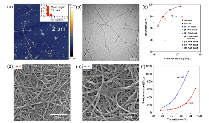
As analyzed above, large-diameter SWCNT bundles in a TCF contribute little to the electrical conductivity but lower the light transmission. Many experimental studies [8,9,32,[99], [100], [101], [102]] have demonstrated that isolated tubes are much better than bundles for constructing high-performance films. Compared to post-treatment methods, it is better to directly synthesize isolated SWCNTs, avoiding the introduction of defects and surfactants [8,9]. In 2015, Kauppinen et al. [8] synthesized an isolated SWCNT network by a FCCVD method. They used a spark discharge generator to generate metal catalysts and controlled their concentration by tuning the discharge voltage. SWCNT networks with over 60% isolated tubes were obtained, as verified by TEM and AFM (Fig. 11(a)). The mean length and diameter of the SWCNTs were 4.0 μm and 1.1 nm, respectively. The SWCNTs were filtered by a porous membrane in the outlet of the reactor and then fabricated into a TCF by a press-transfer method. After HNO3 doping, the TCFs showed a low Rs of ∼63 Ω/sq. at 90% T (FoM = 55.3) for 550-nm light. The high isolation of the SWCNTs in the network is considered to account for this high performance. Recently, our group [9,103] synthesized a carbon-welded isolated SWCNT network by an injection FCCVD method [104]. Networks composed of ∼85% isolated tubes were obtained by tuning the carrier gas, as characterized by TEM observations (Fig. 11(b)). A dry filtration and transfer method was used to fabricate the TCFs. Record low Rs values of 41 Ω/sq. for pristine SWCNT TCFs (FoM = 85.0) and 25 Ω/sq. for HNO3-doped films (FoM = 139.4) at 90% T for 550-nm light were obtained (Fig. 11(c)). The performance of our films is the best to date and rivals ITO on a flexible substrate (Fig. 1, Fig. 11(c)). The high concentration of isolated SWCNTs is an important reason for this ultrahigh performance, because it provides efficient carrier transport paths without “dead mass” leading to extra light absorption.
Fig. 11. Structures and optoelectronic performance of SWCNT samples. (a) AFM image of isolated SWCNTs [
The other method to obtain isolated SWCNTs is to disperse a raw SWCNT sample in a solution, which usually involves ultrasonication and centrifugation processes and the addition of special solvents and dispersants, such as dichloroethane [105], superacid [7], hydrazine [106], ionic and nonionic surfactants [85,107,108], and water soluble polymers [60,109,110]. These chemicals and other treatments can debundle SWCNTs into isolated tubes by shear forces [111]. The isolated SWCNT solution is then used to fabricate TCFs by a wet process [18]. The superacid chlorosulfonic acid (CSA) is a powerful solvent to disperse SWCNTs [7], because it has a high dispersion efficiency without adding any surfactants. Furthermore, the dispersed isolated SWCNTs were simultaneously heavily p-doped. The resulting films showed an excellent performance with a low Rs of 60 Ω/sq. at 90.9% T for 550-nm light, which is the best for SWCNT TCFs obtained by a wet process. However, the CSA-doped SWCNTs are unstable in air and show degraded performance upon prolonged time. Young et al. [85] used SDS to disperse SWCNTs. By using a longer sonication time and a higher centrifugation speed (Arc-I), smaller bundles or isolated tubes were obtained (Fig. 11(d) and (e)). Fig. 11(f) shows that the Arc-I sample has a much better performance than the sample (Arc-II) synthesized using a shorter sonication time and a lower centrifugation speed. As previously mentioned [60], CMC is a water soluble polymer that has shown excellent ability to disperse SWCNTs. TCFs fabricated using SWCNTs dispersed with CMC also had good performance (Fig. 7(d)). Even though wet processes have shown great promise in scaled-up production [2,18], it is hard to obtain high-performance SWCNT TCFs due to the introduction of defects and a shorter tube length caused by the harsh dispersion processes. In addition, further acid treatment was usually needed to remove the insulating dispersants which could simultaneously dope the SWCNTs, although the doping is usually unstable, which means that any effects are not long term.
4.2.2. Tube and bundle connections
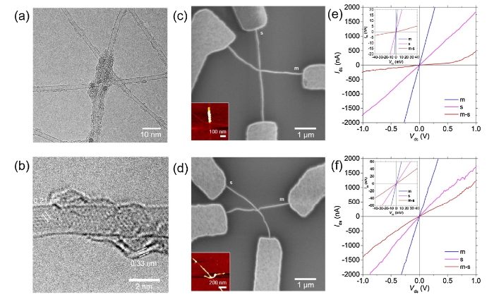
It is well-known that junction resistance is the major contributor to the Rs of SWCNT TCFs, which means that controlling tube or bundle connections may be more important than changing the structure of SWCNTs to improve the performance of SWCNT TCFs. Hassanien et al. [74] studied the effect of the structure of a SWCNT network on the junction resistance between two filaments, which are isolated tubes or small bundles. Fig. 12(a) and (b) shows that the mean resistance of Y-type junctions was ∼58 kΩ, ∼3 times lower than that of X-type junctions. This is because the contact areas of Y-type junctions are much larger than those of X-type ones, which changes the contact from a point to a line. The line contact in Y-type junctions provides much better carrier tunnelling than the point contact of X-type junctions. In addition, all junction resistances >100 kΩ for X-type contacts were found at m- and s-SWCNT junctions (Schottky contacts), which indicated that Schottky contacts were the main contributor for the high junction resistance. Xie et al. [27,83] reported a SWCNT network of mainly Y-type contacts synthesized by an FCCVD method. Fig. 12(c) and (d) show that the bundles in the network are not randomly distributed but preferentially aligned to form Y-type bundles, which is attributed to the gas flow when they grow in the reactor. The Y-type bundled SWCNT TCFs showed excellent performance with a Rs of 50 Ω/sq. at 70% T (FoM = 19.3) for 550-nm light. In addition, mechanical tests showed that the Y-type contacts in the SWCNT network were very strong. Ohno et al. [22] reported high-performance SWCNT thin-film transistors with a carrier mobility of 35 cm2/(V s) and an on/off ratio of 6 × 10⁶. The SWCNT network was composed of Y-type bundled SWCNTs synthesized by a FCCVD method (Fig. 12(e)). They believed that there was strong coupling of carrier wavefunctions at Y-type contacts due to the large contact areas. Thus, the Y-type contacts have a lower junction resistance than the X-type contacts and are therefore preferred for fabricating high-performance SWCNT TCFs. However, controlling the preferential formation of Y-type junctions during SWCNT synthesis is still challenging.
Fig. 12. Junction resistance statistics of (a) X-type and (b) Y-type contacts [
Recently, our group [9] proposed forming a carbon-welded structure at tube junctions to decrease junction resistance, especially for m-/s-SWCNT junctions. We used a high-flux carrier gas to decrease the catalyst concentration and nucleated SWCNTs in a FCCVD reactor, to shorten the growth time. Surplus carbon atoms pyrolyzed from the hydrocarbons preferentially deposited as graphitic carbon, just like the growth of vapor phase-grown carbon fibers [112], at tube junctions to form carbon welds and simultaneously prevent the bundling of SWCNTs by van der Waals forces. Fig. 13(a) shows that at the junctions the tubes are tightly welded by graphitic carbon, and based on TEM observations of >400 intertube junctions the percentage of carbon-welded junctions is estimated to be ∼98%. The graphitic structure of the carbon welds was verified by high-resolution TEM examination (Fig. 13(b)), where a typical graphitic layer structure was observed. In order to verify the effect of carbon welding on the electrical resistivity of the SWCNT networks, isolated SWCNT-based field effect transistors (FETs) were fabricated. Fig. 13(c) and (e) show that the curve of m-s drain current (Ids) versus drain voltage (Vds) behaves nonlinearly for FETs without carbon welding whereas it is almost linear for FETs with carbon welding (Fig. 13(d) and (f)). It is therefore reasonable to conclude that carbon welding between tubes converts Schottky contacts between m- and s-SWCNTs into near-ohmic ones, and therefore greatly lower the Rs of the network. Fig. 11(c) shows that this carbon-welded isolated SWCNT thin film had a superior TCF performance, indicating that this carbon welding is a good way to decrease the junction resistance between tubes in SWCNT networks.
Fig. 13. Structural and electrical characterization of carbon weld. (a) Low- and (b) high-resolution TEM images of isolated SWCNTs with carbon welds. Isolated SWCNT-based FETs (c) without and (d) with carbon weld. (e, f) Ids versus Vds of devices (c) and (d), respectively. Gate voltage Vgs = -10 V [
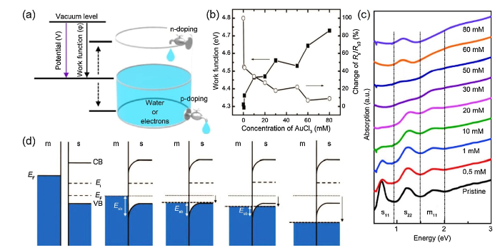
Owing to the unsatisfactory optoelectronic performance of pristine SWCNT TCFs, chemical doping is often used to improve their performance. It is easy to dope SWCNTs because all the carbon atoms are exposed. Actually, as-prepared SWCNT thin films are usually p-doped due to ambient O2 adsorption on the tubes. Many dopants including HNO3, AuCl3, SOCl2, and CSA have been studied, a majority of which are p-dopants as electron-acceptors. In general, chemical doping can lower Rs by a factor of >3, but has little effect on T. Young et al. [26,35,113,114] systematically studied the effects of dopants on the Rs of SWNCT thin films. The doping effect is illustrated as a simple water bucket model (Fig. 14(a)). It can be seen that if the level of the molecule (electrochemical potential) is higher than the surface (Fermi level or work function), electrons will flow into the material (SWCNTs), which corresponds to donating electrons (n-doping) to the SWCNTs. On the contrary, if the electrochemical potential of the molecule is lower than that of the surface, electrons will be drawn out of the material (SWCNTs), which corresponds to accepting electrons (p-doping) from SWCNTs, i.e., placing holes in SWCNTs. As a result, the Fermi level or work function of the SWCNTs will be changed by n- or p-dopants. AuCl3 is a commonly used p-dopant for SWCNTs. Because the reduction potential of Au3+ (1.52 V) is higher than that of SWCNTs, charge transfer from SWCNTs to Au3+ is expected to occur. Fig. 14(b) shows that when a SWCNT thin film is spin-coated with an AuCl3 solution, its work function increases along with the increase of AuCl3 concentration, i.e., the increase of p-doping, which is proven by Raman spectra and absorption spectra (Fig. 14(c)). The Rs value of the SWCNT thin film rapidly decreases when a low concentration of AuCl3 is used, which means that the Fermi level of SWCNTs is very sensitive to the amount of p-doping by AuCl3. When the concentration of AuCl3 is increased, there is little further change in Rs and the final Rs value is ∼1/10 of that of pristine SWCNTs. Some studies [67,74] have argued that p-doping leads to a much larger decrease in junction resistance than the resistance of the tubes. Because the resistance for Schottky contacts in a normal SWCNT network is much higher than those of other-type contacts, the dramatic decrease in Rs for the thin film must be ascribed to the decreased resistance of Schottky contacts. Fig. 14(d) shows that AuCl3 doping gradually lowers the Schottky barrier (Esb) at junctions between m- and s-SWCNTs until Esb is totally eliminated along by the increased AuCl3 concentration. Therefore, the change of the resistance of Schottky contact is consistent with the result shown in Fig. 14(b). The SWCNT TCF after AuCl3 doping had a Rs of 36 Ω/sq. at 85% T (FoM = 61.9) for 550-nm light, which is at the top of SWCNT TCF performance (Fig. 1). The effect of other dopants on the performance of the films is similar to that produced by AuCl3. Representative FoM values for high-performance SWCNT TCFs doped using the following dopants are as follows: HAuCl4 [53] (FoM = 87.1), HNO3 [50] (FoM = 68.3), CSA [7] (FoM = 64.3), and CuI [45] (FoM = 40.5). However, chemical doping is usually unstable. For example, a 15% increase in Rs was observed over the first two days in ambient atmosphere after CSA doping SWCNT TCFs [7]. After accelerated ageing tests (24 h at 85% relative humidity and 85 °C for industrial applications), Rs increased by 220%. Because gaseous or liquid dopants are weakly adsorbed on the surface of SWCNTs and are inherently unstable. They can desorb and evaporate in the air, especially under thermal loading, which leads to the recovered electrochemical potential of the SWCNTs. Furthermore, moisture or other species in the air may react with the strongly oxidizing dopants, which also makes them less effective [18].
Fig. 14. Effects of chemical doping on SWCNTs. (a) Water bucket model for changing the work function (Fermi level) of SWCNTs by n-doping or p-doping [
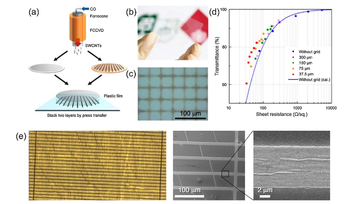
Patterning has also proven to be an effective method of improving the optoelectronic performance of SWCNT TCFs. Ohno et al. [41,46] prepared a micropatterned SWCNT network by putting a micropatterned membrane filter in a FCCVD system (Fig. 15(a-c)). The special network was characterized by its transmittance: T = (A-W)2/A2 + W (2A-W)/(eαtgA2), where A is the period of the grid, W is the width of the grid wire, tg is the thickness (height) of the grid, α is a constant (absorption coefficient), and the left term is the aperture ratio meaning the open area of the microgrid. The equation shows that if the SWCNT grid wire is thick enough (for example 200-nm), the right term will be negligible. Thus, T is simply determined by the aperture ratio. The authors demonstrated that an aperture ratio (T) of >0.95 can be obtained for the micropatterned SWCNT network. They then fabricated a SWCNT TCF which consisted of two layers of a uniform SWCNT thin film and a SWCNT microgrid (Fig. 15(a-c)) [41]. The microgrid decreased the Rs of the TCF while keeping a high T. Fig. 15(d) shows the performance of this special SWCNT TCF after HNO3 doping. It can be seen that Rs of the SWCNT TCF without the microgrid at 80% T for 550-nm light decreases from 95 to 53 Ω/sq. (FoM = 30.1) by adding the microgrid with an A value of 37.5 μm. This work demonstrated the positive effect of patterning SWCNTs on their TCF performance. Later, they replaced the two layers of the SWCNT film with a wire grid of isolated SWCNTs synthesized using improved growth conditions to obtain high-performance SWCNT TCFs (Fig. 15(e)) [46]. After HNO3 doping, the collected patterned TCFs demonstrated excellent TCF performance with a Rs of 29 Ω/sq. at 87% T (FoM = 90.1) for 550-nm light. It is necessary to point out that the Rs was measured by a 2-terminal method. As shown in the left part of Fig. 15(e), the current is supplied in a direction parallel to the horizontal wires. In other words, the resistance along the direction perpendicular to the horizontal wires should be much larger than the measured one. Thus, the Rs of this microgrid patterned SWCNT TCF is anisotropic. In addition, the holes in the pattern may be a problem for future high-resolution display applications.
Fig. 15. Fabrication and characterization of patterned SWCNT TCFs. (a) Schematic of the SWCNT TCF fabrication process with a microgrid. (b) Photograph of a SWCNT TCF with a microgrid. (c) Micrograph of the TCF with a microgrid with a period of 37.5 μm. (d) Optoelectronic performance of SWCNT TCFs with the microgrid for various A values of the grid [
In the past fifteen years, various strategies have been developed to improve the optoelectronic performance of SWCNT TCFs by controlling the SWCNT structure (diameter, length, quality, and electrical type), network configuration optimization (bundle size, and tube and bundle connections), chemical doping, and network patterning. From the above discussion, it is concluded that isolated/small-bundle, heavily doped m- or s-SWCNTs with a large diameter, long length, and high quality are desired for the fabrication of high-performance TCFs. Y-type or welded tube/bundle junctions can greatly decrease the contact resistance at junctions in a SWCNT network. A patterned structure can decrease the Rs of the TCF while maintaining a high T if the aperture ratio is high. Although notable progress has been made, there are still many challenges remaining.
SWCNTs with large diameters have small bandgaps, much high carrier concentrations, and large contact areas at intertube junctions, which give them lower intrinsic and junction resistances. However, it is difficult to obtain high-quality SWCNTs with diameters >2.5 nm. To date, most SWCNTs used for TCF fabrication have diameters in the range of 1-2 nm. Therefore, the preparation large-diameter SWCNTs with high quality is urgently needed. Choosing suitable and novel carbon sources (n-propylbenzene [94], methanol and ethanol [115]), catalysts (gold [116]), growth promoters (thiophene [117]), etchants (water [118]), or higher growth temperature [119] may be effective ways of achieving this. The use of longer SWCNTs can reduce the number of contacts along the carrier transport paths in the networks, however, TCFs composed of ultralong (>100 μm) SWCNTs have not yet been reported. To obtain longer SWCNTs, it is essential to use highly active catalysts with a long catalytic life. At the same time, the residence time of the catalyst in the reaction zone should be as long as possible. In this sense, the use of bimetallic catalysts [120], binary carbon sources [9,54,104], new growth promoters [120], a high growth temperature, and a longer reaction zone may be helpful. Finally, m-SWCNTs are preferred for fabricating high-performance TCFs because of their intrinsically low resistance and the elimination of Schottky contacts in a network. However, the direct synthesis of high-purity m-SWCNTs is still a big challenge because of the lack of a clear growth mechanism and an effective synthesis method [121]. Based on our current understanding, the use of bimetallic (tungsten-cobalt) [122] or metal carbide (molybdenum carbide) [123] catalysts may help to obtain the TCFs enriched with m-SWCNTs.
Large bundles contribute little to the electrical conductivity but lower the light transmission. However, the gathering of SWCNTs into bundles to decrease surface energy is a spontaneous and common phenomenon in their formation. Even though isolated-SWCNT enriched samples have been synthesized, the percentage of isolated tubes needs to be further improved. Y-type SWCNT contacts have a much lower junction resistance than X-type contacts because of their much larger contact areas. However, controlling the types of contacts in SWCNT networks is still challenging, even though gas flow is considered as an important influence [27]. For this reason, the development of new techniques to control junction types based on an understanding of X- and Y-type formation mechanisms is highly desired. Patterning is a good way to decrease the Rs of the TCF while keeping its T almost unchanged. However, the Rs of a microgrid patterned SWCNT TCF may be anisotropic and the large holes (tens of micrometers) in the pattern may be a problem for high-resolution display applications. In future, the development of techniques to construct microgrid patterned SWCNTs with small square holes and highly conductive wires is anticipated.
Chemical doping is widely used to lower the electrical resistivity and change the work function of SWCNT TCFs by injecting holes or electrons into them. However, gaseous or liquid dopants (HNO3, AuCl3, SOCl2, CSA, etc.) are weakly adsorbed on the surface and are inherently unstable. In particular, when SWCNT TCFs are used as transparent electrodes in OLEDs or PVs, exposure to elevated temperatures is inevitable [19], which results in accelerated desorption of dopants from the SWCNTs. More seriously, the desorbed dopants may poison other layers (especially organic) of the devices and hence, greatly lower their performance. Therefore, developing methods to realize the efficient and stable doping of SWCNT TCFs is a challenging and urgent task. CuI particles (∼100-nm diameter) [45] have been reported to be a heavy p-dopant that is stable for over one month in the air. Molybdenum oxide (MoOx)-doped SWCNT TCFs after argon annealing [124] also showed good doping stability for >20 days in the air. However, the particle sizes of the CuI and MoOx need to be made smaller in order to improve the optoelectronic performance of SWCNT TCFs. In addition, a longer working time (months or years) and higher temperature stability are required in real applications. N-doped SWCNTs [125] have shown stable metallic behavior because of the incorporation of N atoms into the graphitic structure of SWCNTs, so that this material may be another solution to improve the performance of SWCNT TCFs.
Although ultrahigh-performance SWCNT TCFs [9] can be obtained by directly welding isolated nanotubes into a network, the efficiency and yield of this synthesis technique are still unsatisfactory. Apart from efficiency and yield, the synthesis of large-area uniform SWCNT TCFs in a continuous manner is equally important for their future commercial applications. Recently, a continuous FCCVD synthesis, gas deposition, and press transfer technique has been reported by our group for fabricating large-area SWCNT thin films [126], yielding meter-scale uniform TCFs. This work has advanced the future industrialization of SWCNT TCFs fabricated by a dry process. The flexibility of SWCNT TCFs is proven to be excellent, however, studies of their stretchability have been less reported in literature and this requires more attention. In sum, SWCNT TCFs have shown promising optoelectronic, mechanical, and chemical properties, and notable progress has been made in recent years. However, there are still challenges remaining from technical and economical viewpoints. Considerably more effort is needed to further advance the development of SWCNT TCFs for their use in flexible and stretchable optoelectronics.
This work was financially supported by the Ministry of Science and Technology of China (Grant No. 2016YFA0200101), the National Natural Science Foundation of China (Grant Nos. 51625203, 51532008, 51572264, 51772303, 51761135122, 51872293), and the Chinese Academy of Sciences (Grant No. 174321KYSB20160011).

 WeChat
/
| 〈 |
|
〉 |
