


Different Diffusion Behavior of Cu and Ni Undergoing Liquid-solid Electromigration
[M.L. Huang1  , Z.J. Zhang
1 , H.T. Ma1 , L.D. Chen2 ]
, Z.J. Zhang|
|


The diffusion behavior of Cu and Ni atoms undergoing liquid-solid electromigration (L-S EM) was investigated using Cu/Sn/Ni interconnects under a current density of 5.0 × 10³ A/cm2 at 250 °C. The flowing direction of electrons significantly influences the cross-solder interaction of Cu and Ni atoms, i.e., under downwind diffusion, both Cu and Ni atoms can diffuse to the opposite interfaces; while under upwind diffusion, Cu atoms but not Ni atoms can diffuse to the opposite interface. When electrons flow from the Cu to the Ni, only Cu atoms diffuse to the opposite anode Ni interface, resulting in the transformation of interfacial intermetallic compound (IMC) from Ni3Sn4 into (Cu,Ni)6Sn5 and further into [(Cu,Ni)6Sn5 + Cu6Sn5], while no Ni atoms diffuse to the opposite cathode Cu interface and thus the interfacial Cu6Sn5 remained. When electrons flow from the Ni to the Cu, both Cu and Ni atoms diffuse to the opposite interfaces, resulting in the interfacial IMC transformation from initial Cu6Sn5 into (Cu,Ni)6Sn5 and further into [(Cu,Ni)6Sn5 + (Ni,Cu)3Sn4] at the anode Cu interface while that from initial Ni3Sn4 into (Cu,Ni)6Sn5 and further into (Ni,Cu)3Sn4 at the cathode Ni interface. It is more damaging with electrons flowing from the Cu to the Ni than the other way.
With the continuous miniaturization of electronic devices, the diameter of solder joints has been downsized to less than 100 μ m, which is known as micro bumps. Meanwhile, the current density through each solder bump is increasing even up to 104 A/cm2, which causes a more serious Joule heating effect during electromigration (EM)[1], [2] and [3]. The solder bumps with low melting point might locally melt under such a serious Joule heating effect and consequently cause early failure of solder joints. The solder melting phenomenon induced by solid-solid electromigration (S-S EM) has become one of the main failure modes[4] and [5]. Due to surface tension, the solder joint maintains its initial shape even after melting, resulting in the transformation of S-S EM into liquid-solid electromigration (L-S EM).
Since the diffusivity of atoms in liquid is several orders of magnitude larger than that in solid[6], the interfacial reaction and failure mechanism induced by L-S EM are greatly different from those induced by S-S EM. For instance, Huang et al.[7], [8] and [9] reported that an abnormal diffusion behavior of Zn atoms was observed in Cu/Sn-9Zn/Cu and Cu/Sn-9Zn/Ni interconnects undergoing L-S EM; Gu and Chan[10] reported that two separate Bi-rich layers formed at the anode when undergoing L-S EM at 140 ° C, but only one Bi-rich layer formed when undergoing S-S EM at 75 ° C; Liao et al.[11] characterized the preferential Pb migration toward the anode in eutectic Sn-Pb molten solder undergoing L-S EM, and the effective charge number of Pb was calculated to be 2.7, which is one order of magnitude lower than the reported value of 47 for self-electromigration in bulk Pb; Huang et al.[12] investigated the interfacial reaction in Cu/Sn-3.5Ag/Cu interconnects undergoing L-S EM, and found that the dissolution rate of the cathode Cu was one order of magnitude faster than that undergoing S-S EM. Since the damage of solder interconnects induced by L-S EM is more serious than that induced by S-S EM, it is critical to understand the fundamental aspects of L-S EM.
The Cu/solder/Ni structure is widely applied in chip interconnects, and previous studies have shown that the Cu-Ni cross-solder interaction occurred and thus affected the interfacial reaction during wetting reaction, solid-solid reaction and S-S EM[5], [13], [14] and [15]. Lin et al.[5] investigated the cross-solder interaction between Cu and Ni in Cu/Sn-37Pb/Ni flip chip solder joints and found that when electrons flowed from the Cu to the Ni, EM-induced failure occurred at the cathode Cu interface, while there was no evidence of microstructure change when the electrons flowed from the Ni to the Cu. Wu et al.[15] reported that EM effects significantly enhance the diffusion rate of Cu when the electrons flowed from the Cu to the Ni, promoting the cross-solder interaction between Cu and Ni in Cu/Sn/Ni interconnects. It is indicated that the EM-induced failure mechanism of Cu/solder/Ni flip chip joints strongly depended on the current direction. However, there is no literature on the Cu-Ni interaction undergoing L-S EM. In the present work, the different diffusion behavior of Cu and Ni atoms as well as Cu-Ni cross-solder interaction in Cu/Sn/Ni interconnects undergoing L-S EM was investigated.
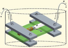
Line-type Cu/Sn/Ni interconnects were prepared by immersion soldering at 250 ° C for 10 s. The EM specimens were prepared in the same way as described in the previous study[16]. The cross-section of EM specimens was 300 μ m × 300 μ m, and the Sn solder between the Cu and Ni substrates was 200 μ m thick. Fig. 1 shows the schematic of the experimental configuration. The EM experiments were conducted in silicone oil under a current density of 5.0 × 10³ A/cm2, and the temperature of EM specimens was maintained at 250 ± 2 ° C, which was monitored by a thermocouple. The EM duration ranged from 10 min to 4 h. Reference experiments without electron current stressing were conducted at the same temperature for comparison.
 | Fig. 1 Schematic of experimental configuration. |
he microstructural evolutions of line-type Cu/Sn/Ni interconnects undergoing L-S EM and L-S reaction were examined by scanning electron microscopy (SEM, JSM-5600LV) operated at 15 keV. Electron probe microanalysis (EPMA, EPMA-1600) was used to identify the compositions of the phases. The area of the interfacial intermetallic compound (IMC) layer was measured using image processing software, and the average thickness was determined by dividing the area by the line length of the interface.
Fig. 2 shows the cross-sectional microstructure of an as-soldered Cu/Sn/Ni interconnect. A Cu6Sn5 layer of 0.30 μ m in thickness formed at the Cu interface, while a Ni3Sn4 layer of 0.25 μ m in thickness formed at the Ni interface. Obviously, no Cu and Ni atoms diffused to the opposite interfaces in the as-soldered Cu/Sn/Ni interconnect, i.e., no Cu-Ni cross-solder interaction occurred during immersion soldering.
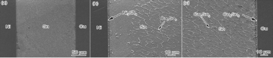 | Fig. 2 Microstructure of as-soldered Cu/Sn/Ni interconnect: (a) macrograph; (b) Ni/Sn interface and (c) Sn/Cu interface. |
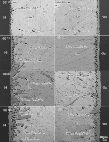
Fig. 3 shows the microstructural evolution of the interfacial IMCs undergoing L-S reaction (without electron current) at 250 ° C for various times. The interfacial IMCs gradually grew thicker with increasing time. After L-S reaction for 10 min (Fig. 3(a) and (b)), Cu atoms dissolved into the solder from the Cu substrate and diffused to the opposite Ni interface, resulting in the interfacial IMC transformation from initial Ni3Sn4 into (Cu0.83Ni0.17)6Sn5. Similar dissolution and diffusion process of Ni atoms also occurred, resulting in the formation of (Cu0.92Ni0.08)6Sn5 instead of Cu6Sn5 at the Cu interface. The average thicknesses of IMCs at the Ni and Cu interfaces were 2.59 μ m and 4.88 μ m, respectively. Additionally, some large IMC particles were observed in the Sn matrix, which precipitated during solidification. After L-S reaction for 1 h (Fig. 3(c) and (d)), the average thicknesses of (Cu0.85Ni0.15)6Sn5 IMC at the Ni interface and (Cu0.90Ni0.10)6Sn5 IMC at the Cu interface grew to 6.89 μ m and 8.26 μ m, respectively. After L-S reaction for 2 h (Fig. 3(e) and (f)), the thicknesses of (Cu0.87Ni0.13)6Sn5 IMC at the Ni interface and (Cu0.92Ni0.08)6Sn5 IMC at the Cu interface continuously increased to 10.33 μ m and 11.31 μ m, respectively. With increasing reaction time to 4 h (Fig. 3(g) and (h)), the average thicknesses of (Cu0.73Ni0.27)6Sn5 at the Ni interface and (Cu0.91Ni0.09)6Sn5 at the Cu interface reached 17.54 μ m and 12.22 μ m, respectively. There was no obvious Cu3Sn layer formed at the Cu interface. Wang et al.[13] investigated the Cu-Ni cross-solder interaction in Cu/Sn/Ni interconnect at 250 ° C and found that the growth of Cu3Sn at the Cu interface was inhibited, which agrees with the results in the present work.
 | Fig. 3 SEM images of Cu/Sn/Ni interconnects after L-S interfacial reaction at 250 ° C without electron current for various times: (a) and (b) 10 min; (c) and (d) 1 h; (e) and (f) 2 h; (g) and (h) 4 h. |
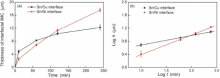
Fig. 4 shows the growth kinetics of IMCs at the Ni and Cu interfaces during reaction at 250 ° C. Fig. 4(a) shows the growth kinetics in linear scale. It is clear that the IMC at the Ni interface was thinner than that at the Cu interface at the beginning, but became thicker after a period of reaction time (about 2 h). Fig. 4(b) shows the growth kinetics in logarithmic scale. The growth kinetics of the IMC at the Cu interface followed a t0.29 relationship with time and that at the Ni interface followed a t0.60 relationship with time. The higher growth rate of IMC at the Ni interface was attributed to that a large amount of Cu atoms dissolved from the opposite Cu substrate and diffused to the Ni interface to form (Cu, Ni)6Sn5.
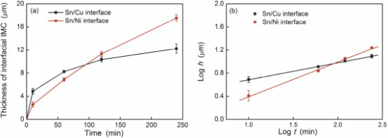 | Fig. 4 Growth kinetics of interfacial IMCs during liquid-solid interfacial reaction at 250 ° C: (a) in linear scale; (b) in logarithmic scale, where h is the thickness of interfacial IMC and t is time. |
According to the Sn-Cu-Ni ternary phase diagram[17], the solubility limits of Cu and Ni in Sn are estimated to be about 1.2 wt% and 0.2 wt%, respectively. It is noted that the solubility limit of Cu is greatly reduced to 0.6 wt% with a small addition of Ni in Sn, while the solubility limit of Ni is little changed even with a addition of 0.6 wt% Cu in Sn but then decreases rapidly if the addition of Cu in Sn is higher than 0.6 wt%. Therefore, if the Cu concentration is higher than 0.6 wt% at the Ni interface, the excessive Cu atoms will instantaneously precipitate as the interfacial Cu-Sn IMC. Consequently, a constant Cu concentration gradient is established across the solder, which generates a Cu atomic flux from the Cu interface to the Ni interface. As long as the dissolution of Ni from the substrate is sufficient at the interface, the Cu atomic flux will exist and the Cu-Sn IMC layer continuously grows at the Ni interface. Similarly, there is a Ni concentration gradient across the solder, which induces a Ni atomic flux from the Ni interface to the Cu interface. Since the concentration gradient of Cu is significantly higher than that of Ni, the Cu atomic flux across the solder is larger than that of Ni across the solder. After diffusing to the opposite sides, both Cu and Ni atoms precipitate in the form of interfacial IMCs. As a result, the IMC at the Ni interface grew thicker than that at the Cu interface with increasing reaction time.
Fig. 5 shows the microstructural evolution of the Cu/Sn/Ni interconnect undergoing EM with electrons flowing from the Cu to the Ni (the diffusion of Cu atoms is called “ downwind diffusion” while that of Ni atoms is called “ upwind diffusion” ).
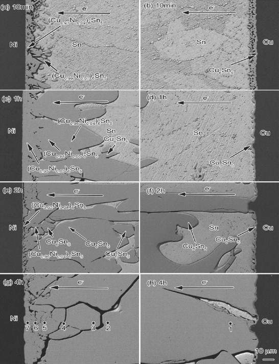 | Fig. 5 SEM images of Cu/Sn/Ni interconnects after EM (electrons flowing from Cu to Ni) for various time: (a) and (b) 10 min; (c) and (d) 1 h; (e) and (f) 2 h; (g) and (h) 4 h. |
At the anode Ni interface, an uneven IMC layer of 8.38 μ m in thickness formed after L-S EM for 10 min (Fig. 5(a)). The composition of the interfacial IMC was identified as (Cu0.91Ni0.09)6Sn5. After L-S EM for 1 h (Fig. 5(c)), some large block interfacial IMC was still (Cu, Ni)6Sn5 with a thickness of 67.51 μ m. After L-S EM for 2 h and 4 h (Fig. 5(e) and (g)), the IMC continuously grew and even protruded across the solder to the cathode Cu. Table 1 shows the compositions of the IMCs across the interconnect. (Cu1-xNix)6Sn5 formed close to the Ni interface and the Cu6Sn5 formed close to the Cu interface. The closer the distance to the anode Ni interface was, the higher the Ni content in (Cu1-xNix)6Sn5 was.
| Table 1 EPMA analysis of the anode interfacial IMCs at different locations in Fig. 5(g) and (h) |
At the cathode Cu interface, short rod-like Cu6Sn5 IMC of 4.41 μ m in thickness formed after L-S EM for 10 min (Fig. 5(b)). Compared with the L-S interfacial reaction case, no Ni atoms could diffuse to the cathode Cu interface since Cu6Sn5 without solid solution of Ni atoms formed. After L-S EM for 1 h and 2 h (Fig. 5(d) and (f)), the thin scalloped interfacial IMCs were still Cu6Sn5 but their thicknesses decreased to 2.05 μ m and 2.04 μ m, respectively. Since no Ni atoms diffused across the liquid solder to the opposite Cu interface, the diffusion of Ni atoms was retarded when Ni atoms were under upwind diffusion.
It is noted that EM significantly enhanced the diffusion of Cu in Sn when Cu atoms were under downwind diffusion, i.e., more Cu atoms were driven to the opposite Ni interface compared with the L-S interfacial reaction case, resulting in the interfacial IMC transformed from Ni3Sn4 into (Cu, Ni)6Sn5 and further into [(Cu, Ni)6Sn5 + Cu6Sn5]; while the diffusion of Ni atoms was significantly retarded when Ni atoms were under upwind diffusion, i.e., no Ni atoms could diffuse to the opposite Cu interface, thus Cu6Sn5 remained at the Cu interface.
 | Fig. 6 shows the microstructural evolution of the Cu/Sn/Ni interconnect undergoing EM with electrons flowing from the Ni to the Cu (the diffusion of Cu atoms is called “ upwind diffusion” while that of Ni atoms is called “ downwind diffusion” ). |
At the cathode Ni interface, a layer (Cu, Ni)6Sn5 of 4.32 μ m in thickness formed after L-S EM for 10 min (Fig. 6(a)). Chen et al.[18] investigated Sn-xCu/Ni interfacial reaction and found that the Cu concentration greatly affected the type of interfacial IMCs. When the Cu concentration was higher than 0.7 wt%, (Cu, Ni)6Sn5 IMC formed at the Ni interface. Obviously, even under upwind diffusion, Cu atoms still diffused to the opposite cathode Ni interface, resulting in the formation of (Cu, Ni)6Sn5 IMCs. After L-S EM for 1 h ( Fig. 6(c)), the interfacial IMC layer was still (Cu, Ni)6Sn5 with a thickness of 8.32 μ m. After L-S EM for 2 h and 4 h ( Fig. 6(e) and (g)), the initial layer (Cu, Ni)6Sn5 transformed into the short rod-like (Cu, Ni)6Sn5, and the thicknesses of interfacial (Cu, Ni)6Sn5 decreased to 2.25 μ m and 2.08 μ m, respectively.
At the anode Cu interface, short rod-like interfacial (Cu, Ni)6Sn5 with a thickness of 16.37 μ m formed after L-S EM for 10 min (Fig. 6(b)). After L-S EM for 1 h (Fig. 6(d)), the interfacial IMC was still (Cu, Ni)6Sn5 with a thickness of 42.92 μ m. Table 2 shows the compositions of the IMCs, and their contents of Cu increased with decreasing distance from the Cu interface. After L-S EM for 2 h (Fig. 6(f)), a new (Ni, Cu)3Sn4 IMC layer formed above (Cu, Ni)6Sn5 IMC. Table 3 shows the composition of the interfacial IMCs, and the total thickness of them increased to 84.97 μ m. After L-S EM for 4 h (Fig. 6(h)), both (Ni, Cu)3Sn4 and (Cu, Ni)6Sn5 significantly grew, and the total thickness of the interfacial IMCs increased to 166.67 μ m. Table 4 shows the compositions of the IMCs. Due to the thickening interfacial IMC at the anode inhibited the diffusion of Cu atoms, few Cu atoms diffused to the anode (Cu, Ni)6Sn5/Sn interface and finally induced the reduction of Cu concentration near the (Cu, Ni)6Sn5/Sn interface. When the Cu concentration was lower than the critical Cu concentration (< 0.3 wt%[18]), (Ni, Cu)3Sn4 IMC instead of (Cu, Ni)6Sn5 IMC formed at the (Cu, Ni)6Sn5/Sn interface. It is interesting to note that an extra Sn layer formed between the interfacial IMC layers at the anode, as shown in between the locations 3 and 4 in Fig. 6(d). Similar results were also observed in Fig. 6(f) and (h). The farther away from the anode Cu was, the higher the Ni content in interfacial (Cu1-xNix)6Sn5 IMCs was, as shown in Table 2, Table 3 and Table 4. The morphology of (Cu1-xNix)6Sn5 IMCs was related to the Ni content, i.e., high Ni content (Cu, Ni)6Sn5 IMCs show a dense short rod-like morphology while low Ni content (Cu, Ni)6Sn5 IMCs show a loose porous morphology. The outer high Ni content (Cu, Ni)6Sn5 layer spalled off and thus a Sn layer formed between them.
| Table 2 EPMA analysis of the anode interfacial IMCs at different locations in Fig. 6(d) |
It is noted that when electrons flowed from the Ni to the Cu, both Cu atoms and Ni atoms could diffuse to the opposite interfaces and participate in the interfacial reaction. The interfacial IMC at the cathode Ni transformed from initial Ni3Sn4 into (Cu, Ni)6Sn5 and further into (Ni, Cu)3Sn4 while the interfacial IMC at the anode Cu transformed from initial Cu6Sn5 into (Cu, Ni)6Sn5 and then into [(Cu, Ni)6Sn5 + (Ni, Cu)3Sn4]. Regardless of the flowing direction of electrons, the growth of interfacial IMCs at the anode was promoted while that at the cathode was restrained. In addition, the growth rate of interfacial IMCs at the anode was one order of magnitude higher than that undergoing L-S interfacial reaction.
| Table 3 EPMA analysis of the anode interfacial IMCs at different locations in Fig. 6(f) |
| Table 4 EPMA analysis of the anode interfacial IMCs at different locations in Fig. 6(g) and (h) |
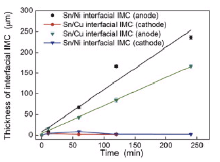
Fig. 7 shows the growth kinetics of interfacial IMCs undergoing EM at 250 ° C. The growth kinetics of the total interfacial IMCs at the anode followed a linear relationship with time undergoing EM, indicating that the growth of interfacial IMCs at the anode was dominated by the reaction process[19]. While the growth behavior of interfacial IMCs at the cathode was different from that at the anode, i.e., the thickness of interfacial IMCs at the cathode increased at the beginning but then decreased with further increasing EM time, which is in agreement with the result of the Cu/Sn/Cu interconnects undergoing S-S EM in previous study[16].
 | Fig. 7 Growth kinetics of interfacial IMCs undergoing EM at 250 ° C under 5.0 × 10³ A/cm2 |
The atomic diffusion flux undergoing EM can be written as follows[20]:
equation(1)
J=Jem+Jchem=-D(∂ C/∂ x)+(CD/kT)ρ jZ* eJ=Jem+Jchem=-D(∂ C/∂ x)+(CD/kT)ρ jZ* e 
where Jem is the flux caused by the electron wind force, Jchem is the flux caused by the chemical potential gradient, C is the atomic density, D is the diffusivity, k is Boltzmann's constant, T is temperature, ρ is the resistivity of liquid Sn, j is the current density, Z* is the effective charge number, and e is the electron charge.
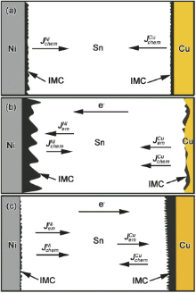
Fig. 8(a) shows the fluxes of Cu and Ni atoms in the Sn matrix during interfacial reaction without electron current. There was only the chemical potential gradient, and thus the atomic fluxes for both Cu and Ni atoms in the liquid Sn can be written as and
, respectively, where
JCuchem and
JNichem are the Cu and Ni atomic fluxes induced by the chemical potential gradient.
 | Fig. 8 Schematic of atomic fluxes in the Cu/Sn/Ni interconnect: (a) L-S interfacial reaction; (b) EM with electrons from Cu to Ni; (c) EM with electrons from Ni to Cu. |
As shown in Fig. 8(b), when electrons flow from the Cu to the Ni, the Cu atomic flux in Sn can be written as


As shown in Fig. 8(c), the Cu atomic flux in the Sn can be written as


1)The flowing direction of electrons significantly influences the Cu-Ni cross-solder interaction undergoing L-S EM, i.e., under downwind diffusion, both Cu atoms and Ni atoms can diffuse to the opposite interfaces; while under upwind diffusion, it is Cu atoms but not Ni atoms that can diffuse to the opposite interface.
2)When electrons flowed from the Cu to the Ni, the interfacial IMC transformed from initial Ni3Sn4 into (Cu, Ni)6Sn5 and further into [(Cu, Ni)6Sn5 + Cu6Sn5] at the anode Ni interface, while no Ni atoms could diffuse to the cathode Cu interface and the interfacial IMC remained as Cu6Sn5. When electrons flowed from the Ni to the Cu, the interfacial IMC transformed from initial Cu6Sn5 into (Cu, Ni)6Sn5 and further into [(Cu, Ni)6Sn5 + (Ni, Cu)3Sn4] at the anode Cu, while the interfacial IMC transformed from Ni3Sn4 into (Cu, Ni)6Sn5 and further into (Ni, Cu)3Sn4 at the cathode Ni.
3)When under downwind diffusion, Ni and Cu substrates seriously dissolved into the liquid solder and the IMCs occupied the whole interconnect after L-S EM for 4 h, since a thin interfacial IMC layer at the cathode cannot serve as an effective barrier. Moreover, it is more damaging with electrons flowing from the Cu to the Ni than that from the Ni to the Cu.
The authors have declared that no competing interests exist.
| [1] |
|
| [2] |
|
| [3] |
|
| [4] |
|
| [5] |
|
| [6] |
|
| [7] |
|
| [8] |
|
| [9] |
|
| [10] |
|
| [11] |
|
| [12] |
|
| [13] |
|
| [14] |
|
| [15] |
|
| [16] |
|
| [17] |
|
| [18] |
|
| [19] |
|
| [20] |
|