

1. Introduction
The demand of energy is increasing day by day. To sustain the energy and also to get rid from the environmental issues, it is necessary to develop a green energy sources such as photovoltaics (PV), hydropower, wind, biomass and geothermal. Among them, photovoltaics is one of the most promising technologies which converts sustainable and clean solar energy directly into electricity. A dye-sensitized solar cell (DSSC) have easy process method and excellent power conversion efficiency which makes them very attractive for low-cost photovoltaic application and flexible device [[1], [2], [3], [4]]. DSSC has achieved certified power conversion efficiency over 14.3% [1]. A classical DSSC's comprises dye absorbed photoanode, electrolyte and counter electrode. Till date, Pt-based catalysts were widely used for the reduction of electrolyte in DSSC owing to excellent electrocatalytic activity. In addition, it acts as mediator in regenerating the sensitizers. The fast carrier transport from CE to the electrolyte (quick reduction reaction of oxidized iodine molecules) will suppress the recombination of electrons in DSSCs which leads to higher power conversion efficiency [[5], [6], [7]]. Industrial applications of Pt based solar cells were hindered because of their cost and the scarcity [[8], [9], [10]]. Previous studies have revealed that the MoS2 based counter electrodes (CE) are suitable for DSSC application due to excellent catalytic property [[11], [12], [13]]. In general, the unit cell of two-dimensional MoS2 molded metal atom (Mo) is sandwiched by two chalcogen atoms (S), where the monolayers of MoS2 is stacked in basal planes (along c-axis) by week van der Waals interactions in hexagonally packed structure. The van der Waals interaction between two layers can be easily fragmented when small ions are interacted with MoS2. Nanostructure MoS2 has more active sites at the edges of the layers, while these sites are catalytically inert. Many experimental and theoretical results have concluded the above statements. In basic, MoS2 was differentiated in three different phases such as 1 T-octahedral metallic phase, 2H and 3R-trigonal prismatic semiconducting phase, the more possible phase of MoS2 was 2H and 1 T [14,15]. The 1 T phase MoS2 exhibits high electrochemical property compared to 2H owing to more active sites in 1 T phase and metallic nature. In practical, numerous studies demonstrate that the catalytically properties are directly related to the conductive property of the catalysts. The basic concept of electrochemical activity, 1 T phase of MoS2 showed good electrochemical property compared to 2H (has high resistivity) [[16], [17], [18]].
Different strategies were employed to synthesis 1 T and 2H phase of MoS2 and they performed two-step with difficult process. For example, the 2H MoS2 phase was changed into 1 T-MoS2 by fast and efficient preparation of exfoliated 2H MoS2 nanosheets by sonication-assisted lithium intercalation method and then exfoliated 2H MoS2 film was treated with Infrared (IR) laser. During IR laser irradiation process, Fan et al. retrained the 2H-MoS2 on the DVD disc [19]. Knirsch et al. obtained 1 T-polytype MoS2 by chemically-exfoliated molybdenum disulfide with diazonium salts [20]. Xu and co-authors studied the reversion process of 2H-MoS2 when microwave irradiated on the Li-ion exfoliated molybdenum disulfide solution (1 T-MoS2) [21]. Geng et al. synthesized pure and stable metallic MoS2 by hydrothermal method. They studied the reaction property of metallic (200 °C) and semiconductor (240 °C) MoS2, at two different reaction temperature [22]. Kang et al. synthesized 1 T phase of MoS2 from the 2H MoS2, when resonant excitation of plasmon modes in Au nanoparticles deposited on a MoS2 monolayer [23]. Eda et al. were synthesized metallic phase of MoS2 by exfoliated process of natural MoS2 with Li atom [24]. Piao et al. synthesized 1 T and 2H phase of WS2 with surfactant associated method for high performance thermoelectric application [25]. In this study, 1 T and 2H phase of MoS2 were synthesized by one-step simple hydrothermal method at same reaction temperature.
Several methods have been approached to fabricate the M-MoS2 and S-MoS2 based CE and their device performance was studied. Such as Geng et al. have synthesized M-MoS2 nanosheets by hydrothermal method at high temperature of 200 °C and S-MoS2 at 240 °C [22]. In another study, Lei et al. have evaluated different morphology of S-MoS2 as CE for DSSCs [26]. Ultrathin S-MoS2 film fabricated by the direct hydrothermal method has reported by Al-Mamun et al. [27]. Patil et al. have prepared S-MoS2 nanosheets on FTO using wet chemical deposition method [28]. Raj et al. developed highly active and reflective vertically aligned S-MoS2 sheets for CE in DSSCs using CVD [29]. Wei et al. studied interesting property of 1 T and 2H phase of MoS2 deposited on FTO glass substrate. In that work, the electrical conductivity of 1 T and 2H phase of MoS2 directly influences the efficiency of DSSC, which can be clearly seen in the efficiency of 1 T and 2H MoS2 [30]. Even though it is a good material, there are some drawbacks in MoS2 based counter electrode. However, the electrical conductivity of semiconductor MoS2 was low. To overcome the above problem, we prepared the different phases of layered MoS2.
In this work, we have synthesized M-MoS2 and S-MoS2 nanosheets by a simple hydrothermal method using CTAB as a surfactant. Further, the samples were characterized by X-ray photoelectron spectroscopy (XPS), Raman, X-ray diffraction (XRD), field emission scanning electron microscopy (FESEM) and high-resolution transmission electron microscope (HRTEM). CE thin film coated by spray coating technique and their catalytic property was studied using cyclic voltammetry analysis. The device was fabricated using M-MoS2 and S-MoS2 based CE and their performance was studied.
2. Experimental procedure
2.1. Materials
Sodium molybdate dehydrate (Na2MoO4∙2H2O, extra pure AR, 99%], thiourea (CH4N2S, extra pure AR, 99%), cetyltrimethylammonium bromide (C19H42BrN, extra pure AR, 99%) and ethanol were purchased from SRL chemicals (India) and Lithium iodide (LiI) (anhydrous, 97.8%), Lithium perchlorate (LiClO4) (anhydrous) and Iodine (I2) (anhydrous, 99.8%) were purchased in Wako Chemicals, Japan. All chemicals were used without further purification.
2.2. Synthesis of layered MoS2 nanosheets
0.01 mol of sodium molybdate dehydrate and 0.06 mol of thiourea was dissolved in 72 mL of deionized water (DI) and continuously stirred for 1 h. Then 0.1 g of CTAB was added to the above solution and stirred for 30 min. The obtained transparent solution was transferred into 100 mL Teflon-lined autoclave and kept at 180 °C for 24 h. The autoclave was cooled down to room temperature; the black precipitate was collected and washed several times with DI water and ethanol. The final product was dried at 60 °C for 12 h. The sample was termed as S-MoS2 respectively. For the synthesis of M-MoS2, the same procedure was repeated without the addition of CTAB. The sample was termed as M-MoS2, respectively.
2.3. Characterization techniques
The obtained products were characterized using an X’pert PRO (PANalytical) advanced X-ray diffractometer with CuKα radiation (λ = 1.5406 Å), with 2θ ranging between 5° and 80°. The morphological and lattice spacing is observed by using a QUANTA FEG field emission scanning electron microscope at an accelerating voltage of 20 kV and a JEOL JEM 2100 F high-resolution transmission electron microscope at an accelerating voltage of 200 kV. Fourier transform infrared (FTIR) spectra were recorded using a JASCO MFT 2000 spectrometer from KBr pellet samples. Raman spectrum was carried out by using a JASCO NR1800 Raman spectrometer equipped with an Nd:YAG laser. XPS was performed by a Shimadzu ESCA 3400. Cyclic voltammetry (CV) was analyzed using the Solartron 1280C electrochemical test system. Current density and voltage (I-V) characteristics were measured at an air mass of AM1.5 (100 mW cm-2 of simulated sunlight) by using a JASCO solar simulator equipped with a Keithley picoammeter.
2.4. Electrocatalytic analysis
The MoS2 film was prepared by spray coating technique. 0.8 g of MoS2 powder was dispersed in 5 mL of ethanol and grained using mortar for 60 min and 3 drops of Triton-X was added and then the above solution make-up into 100 mL solution using ethanol. The solution was ultrasonicated for 30 min and sprayed on FTO (F-doped SnO2) substrate at 150 °C. Finally, MoS2 coated substrate annealed at 200 °C for 3 h under argon atmosphere. Electrochemical studies were measured in three electrode electrochemical work station. As-synthesized MoS2 coated FTO acts as a working electrode. Ag/AgCl and Pt foil as a reference and the anode electrode, respectively. These three electrodes were placed in the electrolyte solution, which contains 1 mM of I2, 10 mM of LiI and 0.1 M of LiClO4 solution. The CV was recorded at different scan rates and 50 consecutive potential sweeps at scan rate 50 mV s-1.
2.5. Cell fabrication
The photoanode (titanium dioxide (TiO2) was coated on fluorine doped tin oxide (FTO) glass by using a spray coating technique and annealed at 500 °C for 2 h. After heat treatment photo anode dipped in a sensitizer di-tetrabutylammonium cis-bis (isothiocyanate) bis (2,2″- bipyridyl-4,4′dicarboxylato) ruthenium II (N719) solution at overnight. M-MoS2 and S-MoS2 based counter electrode were prepared by simple spray coating technique. The detail preparation method of counter electrode was given in electrochemical analysis section. The sensitizer absorbed photoanode and counter electrode was sealed using binding clips. After that iodine-based electrolyte was filled into the cell and the I-V measurement was performed.
3. Result and discussion
Fig. 1 shows the XRD patterns of S-MoS2 and M-MoS2 samples. S-MoS2 and M-MoS2 showed the diffraction peaks at 32.3° and 57.2° corresponded to hexagonal phase and well matched with JCPDS card No. 73-1508. The plane (100) represents the Mo-S edges in vertical planes. It represents the number of S active atoms in the edges site. In addition to that, S-MoS2 showed peaks at 8.7° and 17.27° corresponding to (002) and (004) planes observed due to the expansion of interlayer distance [[31], [32], [33], [34], [35]]. Moreover, the interlayer distance of S-MoS2 increased to 0.95 nm compared to M-MoS2 (0.62 nm) calculated using Bragg’s equation. The expansion of interlayer distance was due to the incorporation of CTA+ ions between the MoS2 layers [[31], [32], [33], [34], [35]]. The plane (002) indicates that MoS2 layers were grown in basal planes. From the XRD results, the interlayer distance of S-MoS2 expansion was confirmed. The long chain CTA+ may be broken during the hydrothermal process and incorporated between the two layers. Compared with experimental data and standard diffraction pattern, the basal plane (c-axis) of S-MoS2 has shifted lower angle side due to the interlayer distance of S-MoS2 (intercalation of CTA+) and in M-MoS2, the basal plane was not observed.
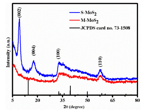
Fig. 1.
XRD pattern of M-MoS2 and S-MoS2.
Fig. 2, Fig. 3 show the XPS spectra of M-MoS2 and S-MoS2 sample. Fig. 2 shows the wide spectra of M-MoS2 and S-MoS2, and the peaks at 161.7, 231.05, 284.8, 394.8 and 531.0 eV corresponds to S, Mo, C, N and O states of the sample, respectively [36]. The high-resolution XPS spectra of Mo 3d is depicted in Fig. 3(a, b), and the two major peaks observed at 227.8 and 231.1 eV are assigned to the Mo 3d5/2 and Mo 3d3/2, respectively. In S-MoS2, the Mo 3d peak was shifted to a higher value of 0.6 eV compared to M-MoS2. It is due to the orientation change of Mo and S atoms in the MoS2 layers. This result indicates that the metallic nature of MoS2 [16,17,[37], [38], [39], [40]]. Fig. 3(c, d) shows that the XPS spectra of S 2p with two broad peaks at 162.1 eV and 160.9 eV corresponds to S 2p3/2 and S 2p1/2 orbital divalent (S2-) sulfur was observed. In the high resolution of S 2p (S-MoS2), the binding energy was shifted to 0.3 eV compared to M-MoS2. The binding energy of the Mo and S atoms have been shifted to higher energy side when M-MoS2 phase changed to S-MoS2 [16,17,[37], [38], [39], [40]]. From the above XPS results, we confirmed the phase transmission in MoS2.
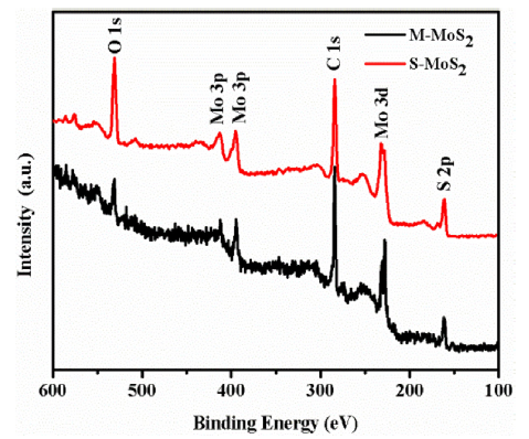
Fig. 2.
XPS survey spectrum of M-MoS2 and S-MoS2.
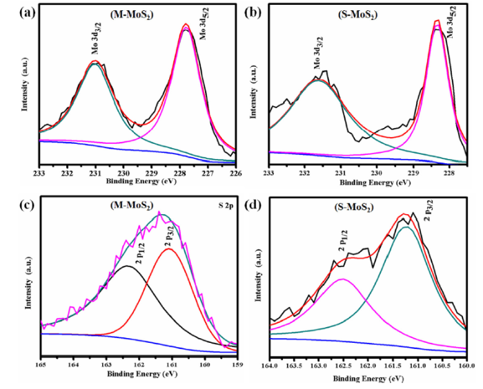
Fig. 3.
(a, c) Core level spectrum of molybdenum and sulphur of M-MoS2 and (b, d) core level spectrum of molybdenum and sulphur of S-MoS2.
Morphology of M-MoS2 and S-MoS2 were investigated by FE-SEM and the results are shown in Fig. 4. From the FE-SEM images, M-MoS2 and S-MoS2 showed sphere-like morphology, where the small MoS2 nanosheets combined together and formed a sphere-like morphology. However, some broken spheres were observed in the M-MoS2 (Fig. 4(a)) with different size from around 0.8 to 1.3 μm. In the case of S-MoS2, the uniform sphere was observed with size of around ∼ 1.1 μm size. Here, surfactant acts as a vital role in the formation of sphere [36]. Fig. 5 shows the TEM and HRTEM images of M-MoS2 and S-MoS2. Fig. 5(a) shows that in M-MoS2, there was no proper formation of a sphere, and the bunch of nanosheets aggregated together to form a broken sphere. The HRTEM image of M-MoS2 revealed that the sample was well crystalline, and the lattice fringes were clearly seen with a d-spacing value of 0.62 nm. Fig. 5(c) shows that in S-MoS2, a sphere was composed of nanosheets with dense interconnected ripples and corrugation was observed. The ripples and corrugation indicates the formation of transparent MoS2 nanosheets on the incorporation of CTAB, as shown in Fig. 5(c). HRTEM image (Fig. 5(d)) shows clear lattice fringes. It confirms the formation of the 2D layered structure of MoS2 with the d-spacing value of 0.95 nm for S-MoS2. HRTEM image confirmed the extension of interlayer distance. The extension value of interlayer distance is 0.33 nm compared to M-MoS2. It equals carbon atom. Here, carbon atom may be intercalated between layers [31]. The obtained FFT pattern indicates the formation of high crystalline nature of the sample (insert image Fig. 4(c, d).
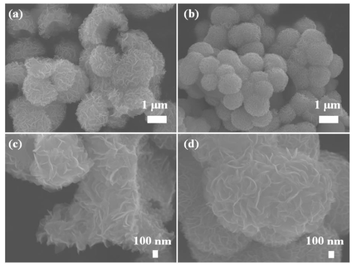
Fig. 4.
(a, c) FE-SEM images of M-MoS2 and (b, d) FE-SEM images of S-MoS2.
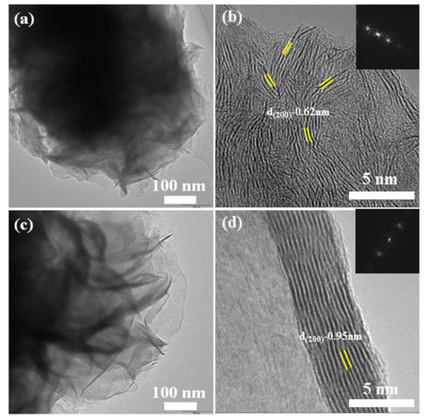
Fig. 5.
(a, b) TEM and HRTEM (insert FFT pattern) images of M-MoS2 and (c, d) TEM and HRTEM (insert FFT pattern) images of S-MoS2.
Fig. 6(a) shows the Raman spectra of M-MoS2 and S-MoS2 samples. The two peaks observed at ∼ 379 and ∼ 405 cm-1 corresponds to the in-plane (E12g) and out-of-plane (A1g) vibration of Mo-S band in the M-MoS2 as shown in Fig. 6(a). In S-MoS2, the position E12g and A1g modes were slightly shifted in lower photon energy. The shift in E12g was due to the absorption of a photon in CTAB molecules and A1g was due to the deceased interlayer van der Waals force [41]. Fig. 6(b) shows the FTIR spectrum of S-MoS2 samples. The peak at 463 and 620 cm-1 was assigned to Mo-S vibration and the peaks indicated the formation of MoS2 [42,43]. The peaks at 2998, 2937 and 1412 cm-1 were attributed to symmetric and anti-symmetric of C-H vibrations. The vibrations at 1568 and 1148 cm-1 indicated the presence of NH and CN band. The absorption band at 3417 cm-1 is due to the OH band vibration. For S-MoS2, the peak at 885 cm-1 was assigned to the CH3 band, which confirmed the incorporation of CTA+ in MoS2 nanosheets [32,41,44].
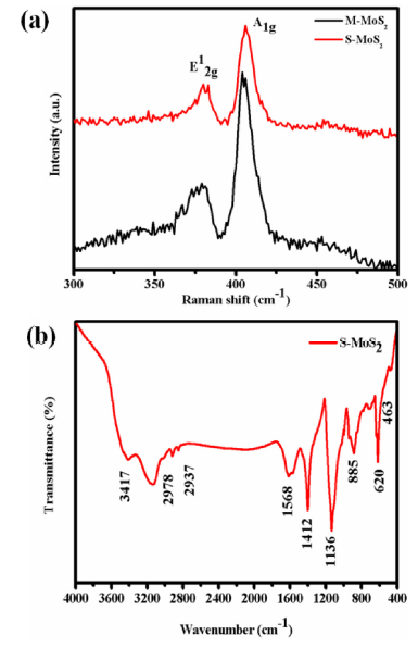
Fig. 6.
(a) Raman spectrum of M-MoS2 and S-MoS2 and (b) FT-IR spectrum of S-MoS2.
Fig. 7 shows the schematic diagram of the catalytic mechanism of the reduction process. The CE was fabricated by spray coat technique and it was briefly described in the experimental section. The electrochemical property of as-fabricated counter electrodes and Pt were evaluated by using three electrode electrochemical work station. In the reduction process, M-MoS2 and S-MoS2 have absorbed the oxidized iodide (I3-). The electron (2e-) was injected from MoS2 layers into oxidized iodide. Finally, it converted into iodide (3I-). The CV analysis is a useful tool to study the catalytic activity of oxidation and reduction reaction of the fabricated electrode. In the CV analysis, the current density and the peak separation between anodic and cathodic (Epp) determine the catalytic property of the materials. M-MoS2, S-MoS2 and Pt counter electrodes were studied for the catalytic property of reduction reaction using CV at a scan rate 50 mV s-1 as shown in the Fig. 8(a). In the CV analysis, all the three electrodes show a similar pair of redox peaks, which correspond to oxidation and reduction process of iodide redox species as shown in Eqs. (1) and (2).
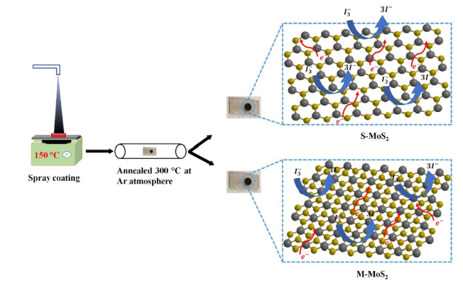
Fig. 7.
Schematic diagram of counter electrode.
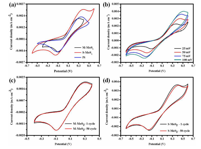
Fig. 8.
(a) CV curves of M-MoS2, S-MoS2, and Pt at scanning rate 50 mV/s, (b) various scanning rates (25, 50, 75 and 100 mV/s) for S-MoS2, (c) CV curves of M-MoS2 at 1st and 50th cycle (scan rate: 50 mV/s) and (d) CV curves of S-MoS2 at 1st and 50th cycle (scan rate: 50 mV/s).
The Epp of the synthesized M-MoS2, S-MoS2 and Pt are 468.28, 540.87 and 467.65 mV, respectively. The M-MoS2 exhibits superior catalytic property than S-MoS2 and similar to Pt counter electrode due to the metallic nature of M-MoS2. The electrocatalytic property of S-MoS2 was lower compared to other CE and the current density was high. This is due to more active sites in the layered structure of sample S-MoS2. Additionally, high catalytic M-MoS2 CE sample was analysed at different CV scanning rates (25, 50, 75 and 100 mV s-1) as shown in Fig. 8(b). The Epp at different scan rate were 466 for 25 mV s-1, 632 for 50 mV s-1, 692 for 75 mV s-1 and 742 for 100 mV s-1, respectively. The Epp and peak current density were linearly increased with incresing scanning rates. The cathodic and anodic peak position and current density was also linearly shifted with increasing scan rate. This linear relationship indicates the redox reaction on M-MoS2 CE and S-MoS2 CE and no specific interaction between I-/I3- redox couples. Fig. 8(c, d) shows the electrochemical stability of synthesized M-MoS2 and S-MoS2 samples. It was measured 50 consecutive cycles at a scanning rate of 50 mV s-1. There is no significant difference in curve shape, Epp and current density value. From the CV analysis, the M-MoS2 exhibits excellent electrochemical property compared to the S-MoS2 electrode. Here, orbital of Mo and S atoms are coupled together due to the hybridization of Mo 3d and S 2p orbitals. When hybridization occurred, the conduction and valence band of the atom was mingled and it could improve the charge transfer kinetics in M-MoS2 [17,18,[45], [46], [47]]. Fig. 9 shows the current density‒voltage (J‒V) characteristic of DSSC with Pt, M-MoS2, S-MoS2 as CE. Photovoltaic parameter such as open circuit voltage (V), short circuit current density (Jsc), fill factor (FF) and power conversion efficiency (η) of solar cells are summarized in Table 1. Efficiency (η) of the DSSCs is 2.52 for Pt, 1.61% for M-MoS2 and 1.29% for S-MoS2, respectively. The results clearly show that the M-MoS2 CE has better performance compared with S-MoS2 owing to metallic nature of M-MoS2. The electrical conductivity was increased in M-MoS2 (6.89 mA cm-2) compared to S-MoS2 CE (5.31 mA cm-2). For comparison, commercial Pt was used as a counter electrode and its electrochemical and photovoltaic performance were performed. Pt CE shows a bit higher electrocatalytic and photovoltaic performance compared to M-MoS2 due to high electrical and electrochemical property. And, the reflective nature of Pt is high compared to MoS2. However, the Pt has a very high cost, and is very rare earth metal. So, we need to go for alternative metal with low cost and high availability. Molybdenum will be a reliable and alternative electrode of Pt CE in DSSCs. The cost of the Pt (27.843 USD/g) is nearly 1000 times higher than molybdenum (0.024 USD/g). Nevertheless, M-MoS2 will be full-filling the new kind of CE for DSSC instead of Pt due to abundant nature, low-cost, and simple fabrication technique.
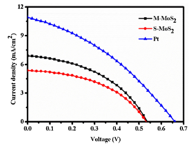
Fig. 9.
IV curve of M-MoS2, S-MoS2, and Pt.
Table 1 Photovoltaic parameters of M-MoS2, S-MoS2, and Pt.
| Counter electrode | Jsc (mA/cm2) | Voc (V) | FF | η (%) |
|---|---|---|---|---|
| M-MoS2 | 6.89 | 0.53 | 0.43 | 1.61 |
| S-MoS2 | 5.31 | 0.53 | 0.45 | 1.29 |
| Pt | 10.98 | 0.65 | 0.50 | 2.51 |
4. Conclusion
In summary, M-MoS2 and S-MoS2 were synthesized by a simple hydrothermal method. The surfactant (CTAB) was used to change phase from M-MoS2 to S-MoS2 during the hydrothermal process and it was verified in XPS spectra. Electrocatalytic activity was investigated in which the anodic and cathodic peak separation (Epp) values of the counter electrode (CE) at 468.28 (M-MoS2) and 540.87 mV (S-MoS2). The electrocatalytic activity and good electrochemical stability were enhanced for M-MoS2 compared to S-MoS2 due to more active sites and electronic conductivity. The power conversion efficiency of M-MoS2 CE (1.61%) based device exhibits higher efficiency compared to S-MoS2 CE (1.29%) based device. The conductivity of M-MoS2 will play the role in enhancing the electrochemical property and as well as device efficiency.
Reference

 WeChat