

1. Introduction
Since the discovery of graphene, 2D materials family has expanded rapidly and inspired extensive attention due to multitudinous fascinating properties of quantum confinement effect, novel excitonic effect and unique electronic transport properties originating from atomic planar structures [[1], [2], [3], [4], [5], [6], [7]]. In past decades, 2D layered materials, such as graphene, MoS2 and Bi2O2Se, perform extremely excellent optoelectronic performance due to high carrier mobility, strong light-matter interactions and adjustable band gap [[8], [9], [10], [11], [12], [13]]. Especially in the field of photoelectric detection, 2D materials have shown a high key device performance of responsivity (R), external quantum efficiency (EQE) and detectivity (D*) due to the special photogating effect in low-dimensional materials [8,11,14]. Recently, 2D ternary materials with a crucial freedom degree of stoichiometry variation have made some excited processes in electronic and optoelectronic devices [[14], [15], [16], [17]]. The bandgap, carrier mobility and other physical or chemical properties can be effectively controlled by adjusting the stoichiometry variation, which can further optimize the device performance [14,15].
BiOBr, as a promising ternary wide-bandgap semiconductor, possesses a huge bandgap of >2 eV and has been reported in photocatalytic field due to the nontoxicity, high light absorption and air stability [18,19]. The wide bandgap put it has great potential for UV applications. However, BiOBr flakes were usually fabricated by liquid methods, exhibiting a poor performance of electronic devices due to the organic contamination, defects, polycrystal and huge thickness [[19], [20], [21], [22], [23]]. In contrast, chemical vapor deposition (CVD) is a valid way to grow high-quality 2D nanostructures by accurately controlling the key growth parameter, and has been widely adopted to obtain 2D semiconducting materials for high-performance optoelectronic devices [8,22,[24], [25], [26], [27], [28], [29]].
In this work, ultrathin 2D BiOBr single-crystalline nanosheets were synthesized by space-confined CVD method. The high crystalline, pure phase were demonstrated by various characterizations of Raman, X-ray photoelectron spectroscopy (XPS) and transmission electron microscopy (TEM). UV photodetectors based on BiOBr nanosheets show excellent device properties of low Idark (1.46 pA) and high R, EQE and D* of 14.96 A W-1, 5460%, and 5.74 × 10¹⁰ Jones, respectively, along with the fast rise time of 80 ms and decay time of 40 ms.
2. Experimental
2.1. CVD growth of 2D BiOBr nanosheets
BiBr3 powder and oxygen were used as the source to synthesize BiOBr nanosheets by a space-limited CVD method. Two mica substrates superimposed on each other were placed on quartz boat in the center of the heating area. And the BiBr3 of 50 mg was placed directly below the mica substrates about 2 cm away. Before growth, the quartz tube was evacuated to 0.1 Pa by vacuum bump. Then, argon gas was aerated into the quartz tube up to atmospheric pressure in order to remove oxygen and water in the quartz tube. After that, 0.1 sccm oxygen and 50 sccm argon were aerated into the quartz tube, and the heating area was heated to 400 ℃ within 10 min and kept growth temperature for 10 min. Finally, the quartz tube was cooled down to room temperature quickly, and the ultrathin BiOBr nanosheets will be obtained on the intercalation of mica substrates.
2.2. Photodetectors fabrication
Firstly, BiOBr nanosheets were transferred from mica substrates to SiO2/Si by a dry transfer process. As-grown BiOBr flakes were spin-coated with poly(methyl methacrylate) (PMMA) at 3500 r s-1 for 1 min and baked at 150 °C for 5 min. After natural cooling, polypropylene carbonate (PPC) (15 wt.%) was covered on the sample at 2000 r s-1 for 60 s and heated at 130 °C for 15 min. Whereafter, the organic film with BiOBr was torn by tweezers and transferred to the SiO2/Si substrate. After that, the organic film adhered to the SiO2/Si substrate was heated at 150 °C for 1 h. Finally, the organic film was removed by acetone at 60 ℃. PMMA and PPC were used as protective layer and transfer layer in the transferred process, respectively. Then, standard EBL process was used to get a patterned PMMA. The Cr/Au electrodes (8/80 nm) were evaporated on the patterned PMMA by thermal evaporation. Finally, acetone was used to remove superfluous organic film with the attached gold to obtain our device.
3. Results and discussion
Fig. 1(a) exhibits the crystal structure of BiOBr which can be indexed to the P4/nmm space group with tetragonal PbFCl-type structure. The typical optical image of 2D square BiOBr nanosheets synthesized by space-confined CVD methods with a high yield is shown in Fig. 1(b). The corresponding atomic force microscope (AFM) image (inset in Fig. 1(b)) shows the atomic level smooth surface of the BiOBr nanosheet with a thickness of 17 nm. As shown in Fig. 1(c), the SEM image of BiOBr nanosheets exhibits the typical 2D square structure. Analogously, smooth surface of the (001) plane can be observed very obviously, demonstrating that the high-quality 2D BiOBr nanosheets are synthesized. Fig. 1(d) shows the typical Raman spectrum from 100 to 180 cm-1 of BiOBr nanoflakes on the SiO2/Si substrate. The obvious two peaks at 110.5 and 155 cm-1 can be observed in Raman spectrum, which are corresponding to the in-plane A1g Bi-Br stretching mode and in-plane Eg Bi-Br stretching mode, respectively. The Raman spectrum is consistent with the previously reported layered BiOBr nanoplates growing along the (001) plane. To further determine the crystallinity and quality of the as-obtained material, the high-resolution transmission electron microscope (HRTEM) image of 2D BiOBr nanosheets is shown in Fig. 1(e). The interplanar spacing of the (001) lattice plane is 0.28 nm, consistent with previous reports. Clear and bright square lattice of corresponding FFT picture (Fig. 1(f)) demonstrates the perfect single crystalline.
Fig. 1.
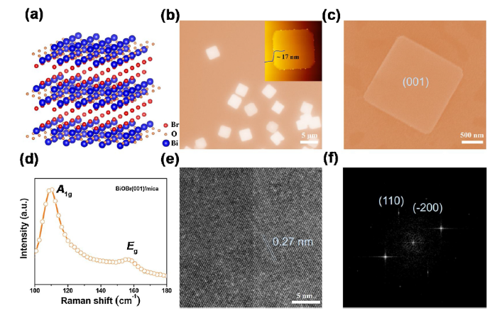
Fig. 1.
(a) Crystal structure of BiOBr. (b) Optical image of 2D BiOBr flakes on mica substrate. The inset figure is the AFM image and height profile of BiOBr flake. (c) SEM, (d) Raman, (e) HRTEM image, and (f) FFT pattern of BiOBr flake.
Fig. 2(a-d) show the composition and bonding types of the as-transferred BiOBr nanosheets on the Si substrates characterized by XPS. The binding energies of Bi 4f5/2 and Bi 4f7/2 peaks are observed at 165 and 160 eV, and the Br 3d peak located at 68.5 eV are attributed to the binding energy of Br 3d5/2 and Br 3d3/2 peaks, respectively. The O1 s spectrum shows two peaks origin from SiO2 and BiOBr, respectively. All the peaks are consistent with the reported values for BiOBr. Full XPS spectrum reveals that the sample has no impurities, indicating the high-quality and high-purified BiOBr crystals fabricated by CVD methods. Fig. 2(e) shows the UV-vis absorption spectrum of 2D BiOBr nanosheets with an apparent absorption peak around 417.71 nm. In order to determine the bandgap of BiOBr, the data can be extracted by using Eq. (1):
Fig. 2.
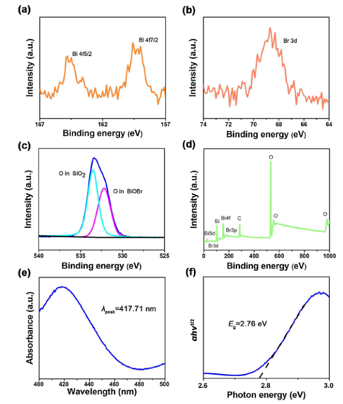
Fig. 2.
XPS spectra of as-transferred BiOBr flakes on SiO2/Si substrate: (a) Bi 4f; (b) Br 3d; (c) O 1s; (d) full spectra; (e) Microscopic UV-vis absorption spectrum; (f) αhv1/2-Eoptical curve of 2D BiOBr nanosheets. The tangent line of the linear region for obtaining the optical bandgap.
where α is the effective absorption coefficient of material, h is the Planck's constant, C is a constant, Eg is the optical bandgap energy of material, k is the index (kindirect = 0.5, kdirect = 2). Based on the above equation, the αhv1/2-Eoptical curve was plotted and shown in Fig. 2(f). We extend tangent line on linear region of Fig. 2(f) and estimated the Eg to be ∼2.76 eV.
Dry-transferred 2D BiOBr-based photodetectors were manufactured on Si substrates by EBL process. Fig. 3(a) shows the schematic diagram of the photodetector under the UV light. The device area is 6.73 μm2. Fig. 3(b) performs a typical current-voltage (I-V) curve under illumination with different wavelengths of 325 and 340 nm, and in the dark. The rectifying-like behavior can be attributed to the Schottky barrier at the contact interfaces due to a huge difference in the work function of Au and BiOBr. And the dark current is 1.46 pA under -10 V bias. To verify the stability of the device, the periodic light (340 nm) with an interval of 20 s was applied on the BiOBr-based photodetector. As shown in Fig. 3(c), the stable current change with incident light on/off operation confirms the long-term cyclability and stability of the BiOBr-based photodetectors. Fig. 3(d) shows a complete current up and down process. The rise time (τrise) and decay time (τdecay) are calculated to be about 80 and 40 ms, respectively, which are much faster than those of other 2D materials-based photodetectors such as MoS2 (9000 ms), [5] ReSe2 (8410 ms) [25], and InSe (4000 ms) [30].
Fig. 3.
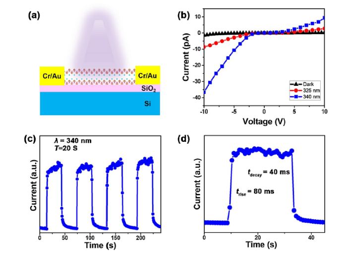
Fig. 3.
(a) Schematic diagram of BiOBr-based UV photodetector. (b) I-V curves in the dark and under illumination with different wavelength irradiation. (c) Time-resolved photoresponse of the device at Vds = 10 V under 340 nm light. (d) A typical photoresponse time curve for rise time and decay time.
In order to further explore the device performance, Fig. 4(a) exhibits the |I|-|V| curves (0 V to -10 V) of the BiOBr-based photodetector under 340 nm light with different intensities ranging from 0 to 225 μw cm-2. As can be seen, the photocurrent increases with the enhanced light power. In addition, the corresponding power and photocurrent at -10 V was fitted with the power law of Iph-Pθ (Fig. 4(b)). The sublinear fitting result (θ = 0.42) indicates the existence of trap states on the surface of the as-synthesized BiOBr flakes ascribed to the defects or vacancies. In order to better compare the performance of different kinds of UV detectors, the critical parameters of R, EQE and D* were calculated to evaluate the photodetecting performance of BiOBr-based photodetector through Eqs. (2), (3), (4):
Fig. 4.
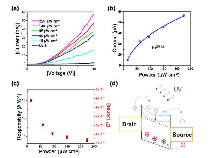
Fig. 4.
(a) Power-dependent |I|-|V| curve under 340 nm light irradiation; (b) Corresponding fitting curve between light power density and photocurrent; (c) The calculated R, D* of BiOBr based photodetectors; (d) Schematic diagram of photogating process by h-trapped states.
where Ilight=Icurrent-Idark is the photocurrent, Icurrent is the total current under the light, Idark is dark current, P is the optical power density, and S is the area of the device, h is the Planck’s constant, c is the velocity of light, λ is the wavelength of incident light and e is the charge of unit electron). The R and D* of the BiOBr-based photodetectors irradiated under 340 nm with different optical power are shown in Fig. 4(c). Apparently, R and D* are improved with the reduced optical power ascribed to the photogating effect by inherent h-trapped states of BiOBr. The h-trapped states can cause an analogous gate voltage to enormously improve the photogain and photoconduction, which can achieve a high device performance of R, EQE and D* (Fig. 4(d)). The max device performance of R, EQE and D* can be calculated to 14.96 A W-1, 5460%, 5.74 × 10¹⁰ Jones, respectively, when the light power is 15 μW cm-2, which is better than those of the other reported 2D UV photodetectors [25,[30], [31], [32]].
4. Conclusion
In summary, high-quality 2D BiOBr nanoflakes were prepared by space-confined CVD method. Contrary to the materials obtained by traditional hydrothermal synthesis method, the space-confined CVD grown BiOBr nanoflakes show an extremely high crystalline quality and excellent UV photodetecting performances. The photodetectors based on the ultrathin BiOBr flakes show ultrahigh R of 14.96 A W-1, EQE of 5460%, and D* of 5.74 × 10¹⁰ Jones, respectively, demonstrating its greatly promising applications in UV optoelectronic devices.
Acknowledgements
This work was financially supported by the National Natural Science Foundation of China (No. U0634002) and the National Basic Research Program of China (No. 2003CB314701).
Reference
DOI
URL
PMID
[Cited within: 1]

The remarkable properties of graphene have renewed interest in inorganic, two-dimensional materials with unique electronic and optical attributes. Transition metal dichalcogenides (TMDCs) are layered materials with strong in-plane bonding and weak out-of-plane interactions enabling exfoliation into two-dimensional layers of single unit cell thickness. Although TMDCs have been studied for decades, recent advances in nanoscale materials characterization and device fabrication have opened up new opportunities for two-dimensional layers of thin TMDCs in nanoelectronics and optoelectronics. TMDCs such as MoS(2), MoSe(2), WS(2) and WSe(2) have sizable bandgaps that change from indirect to direct in single layers, allowing applications such as transistors, photodetectors and electroluminescent devices. We review the historical development of TMDCs, methods for preparing atomically thin layers, their electronic and optical properties, and prospects for future advances in electronics and optoelectronics.
DOI
URL
PMID
[Cited within: 1]
DOI
URL
PMID
[Cited within: 3]
A long-wavelength infrared photodetector based on two-dimensional materials working at room temperature would have wide applications in many aspects in remote sensing, thermal imaging, biomedical optics, and medical imaging. However, sub-bandgap light detection in graphene and black phosphorus has been a long-standing scientific challenge because of their low photoresponsivity, instability in the air, and high dark current. In this study, we report a highly sensitive, air-stable, and operable long-wavelength infrared photodetector at room temperature based on PdSe2 phototransistors and their heterostructure. A high photoresponsivity of approximately 42.1 AW(-1) (at 10.6 mum) was demonstrated, which is an order of magnitude higher than the current record of platinum diselenide. Moreover, the dark current and noise power density were suppressed effectively by fabricating a van der Waals heterostructure. This work fundamentally contributes to establishing long-wavelength infrared detection by PdSe2 at the forefront of long-IR two-dimensional-materials-based photonics.
DOI
URL
PMID
[Cited within: 1]
BiOBr nanosheets with highly reactive {001} facets exposed were selectively synthesized by a facile hydrothermal method. The inner strain in the BiOBr nanosheets has been tuned continuously by the pH value. The photocatalytic performance of BiOBr in dye degradation can be manipulated by the strain effect. The low-strain BiOBr nanosheets show improved photocatalytic activity. Density functional calculations suggest that strain can modify the band structure and symmetry in BiOBr. The enhanced photocatalytic activity in low-strain BiOBr nanosheets is due to improved charge separation attributable to a highly dispersive band structure with an indirect band gap.
DOI
URL
PMID
[Cited within: 2]
Two-dimensional crystals with a wealth of exotic dimensional-dependent properties are promising candidates for next-generation ultrathin and flexible optoelectronic devices. For the first time, we demonstrate that few-layered InSe photodetectors, fabricated on both a rigid SiO2/Si substrate and a flexible polyethylene terephthalate (PET) film, are capable of conducting broadband photodetection from the visible to near-infrared region (450-785 nm) with high photoresponsivities of up to 12.3 AW(-1) at 450 nm (on SiO2/Si) and 3.9 AW(-1) at 633 nm (on PET). These photoresponsivities are superior to those of other recently reported two-dimensional (2D) crystal-based (graphene, MoS2, GaS, and GaSe) photodetectors. The InSe devices fabricated on rigid SiO2/Si substrates possess a response time of approximately 50 ms and exhibit long-term stability in photoswitching. These InSe devices can also operate on a flexible substrate with or without bending and reveal comparable performance to those devices on SiO2/Si. With these excellent optoelectronic merits, we envision that the nanoscale InSe layers will not only find applications in flexible optoelectronics but also act as an active component to configure versatile 2D heterostructure devices.
DOI
URL
PMID
[Cited within: 1]
The first GaS nanosheet-based photodetectors are demonstrated on both mechanically rigid and flexible substrates. Highly crystalline, exfoliated GaS nanosheets are promising for optoelectronics due to strong absorption in the UV-visible wavelength region. Photocurrent measurements of GaS nanosheet photodetectors made on SiO2/Si substrates and flexible polyethylene terephthalate (PET) substrates exhibit a photoresponsivity at 254 nm up to 4.2 AW(-1) and 19.2 AW(-1), respectively, which exceeds that of graphene, MoS2, or other 2D material-based devices. Additionally, the linear dynamic range of the devices on SiO2/Si and PET substrates are 97.7 dB and 78.73 dB, respectively. Both surpass that of currently exploited InGaAs photodetectors (66 dB). Theoretical modeling of the electronic structures indicates that the reduction of the effective mass at the valence band maximum (VBM) with decreasing sheet thickness enhances the carrier mobility of the GaS nanosheets, contributing to the high photocurrents. Double-peak VBMs are theoretically predicted for ultrathin GaS nanosheets (thickness less than five monolayers), which is found to promote photon absorption. These theoretical and experimental results show that GaS nanosheets are promising materials for high-performance photodetectors on both conventional silicon and flexible substrates.

 WeChat