Search for articles:
Wufan Chen, Xin Yan
Corresponding authors:
Received: 2019-09-15
Revised: 2019-10-30
Accepted: 2019-11-17
Online: 2020-04-15
Copyright: 2020 Editorial board of Journal of Materials Science & Technology Copyright reserved, Editorial board of Journal of Materials Science & Technology
More
Abstract
Electronic skin (e-skin) and flexible wearable devices are currently being developed with broad application prospects. Transforming electronic skin (e-skin) into true "skin" is the ultimate goal. Tactile sensing is a fundamental function of skin and the development of high-performance flexible pressure sensors is necessary to realize thus. Many reports on flexible pressure sensors have been published in recent years, including numerous studies on improving sensor performance, and in particular, sensitivity. In addition, a number of studies have investigated self-healing materials, multifunctional sensing, and so on. Here, we review recent developments in flexible pressure sensors. First, working principles of flexible pressure sensors, including piezoresistivity, capacitance, and piezoelectricity, are introduced, as well as working mechanisms such as triboelectricity. Then studies on improving the performance of piezoresistive and capacitive flexible pressure sensors are discussed, in addition to other important aspects of this intriguing research field. Finally, we summarize future challenges in developing novel flexible pressure sensors.
Keywords:
1.Introduction . . . . . . . . . . . . . . . . . . . . . . . . . . . . . . . . . . . . . . . . . . . . . . . . . . . . . . . . . . . . . . . . . 176
2. Flexible pressure sensors . . . . . . . . . . . . . . . . . . . . . . . . . . . . . . . . . . . . . . . . . . . . . . . . . . . . . . . 176
3. Piezoresistive pressure sensors . . . . . . . . . . . . . . . . . . . . . . . . . . . . . . . . . . . . . . . . . . . . . . . . . . 176
3.1. Fabricating of microstructured flexible substrates . . . . . . . . . . . . . . . . . . . . . . . . . . . . . . . . . . 177
3.2. Fabricating of elastic porous conductive materials. . . . . . . . . . . . . . . . . . . . . . . . . . . . . . . . . . 178
3.3. Other designs . . . . . . . . . . . . . . . . . . . . . . . . . . . . . . . . . . . . . . . . . . . . . . . . . . . . . . . . . . . . . 180
4. Capacitive pressure sensors . . . . . . . . . . . . . . . . . . . . . . . . . . . . . . . . . . . . . . . . . . . . . . . . . . . . . 181
4.1. Fabricating of microstructured dielectric layer and electrode . . . . . . . . . . . . . . . . . . . . . . . . . . 182
4.2. Field effect transistors(FETs) type . . . . . . . . . . . . . . . . . . . . . . . . . . . . . . . . . . . . . . . . . . . . . . 183
4.3. Others . . . . . . . . . . . . . . . . . . . . . . . . . . . . . . . . . . . . . . . . . . . . . . . . . . . . . . . . . . . . . . . . . . . 184
5. Piezoelectric pressure sensors . . . . . . . . . . . . . . . . . . . . . . . . . . . . . . . . . . . . . . . . . . . . . . . . . . . 185
6. Further exploration of flexible pressure sensors . . . . . . . . . . . . . . . . . . . . . . . . . . . . . . . . . . . . . 186
7. Conclusions and outlooks . . . . . . . . . . . . . . . . . . . . . . . . . . . . . . . . . . . . . . . . . . . . . . . . . . . . . . 186
Acknowledgments . . . . . . . . . . . . . . . . . . . . . . . . . . . . . . . . . . . . . . . . . . . . . . . . . . . . . . . . . . . . . . 186
References . . . . . . . . . . . . . . . . . . . . . . . . . . . . . . . . . . . . . . . . . . . . . . . . . . . . . . . . . . . . . . . . . . . 187
Electronic skin and flexible wearable devices are two important components of flexible electronic technology [1,2]. Development of electronic skin is motivated by growing interest in artificial intelligence, human-machine interfaces, and prosthetic skin [[3], [4], [5]]. Moreover, flexible wearable devices have great potential for use in health monitoring and nursing applications [6,7]. Electronic skin should mimic sensing capabilities of the skin, and for this reason, realizing electronic skin and flexible wearable devices will depend on the successful development of flexible sensors, including pressure and temperature sensors [8], strain sensors [9], and humidity sensors [10]. Clearly, high-performance flexible sensors will be key to the realization of electronic skin and flexible wearable devices.
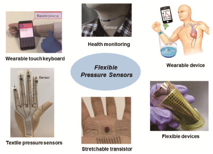
Tactile sensing is one of the fundamental functions of skin, therefore, developing electronic skin that effectively senses touch is key, but will rely on flexible high-performance pressure sensors. Fig. 1 shows flexible pressure sensors and their applications in electronic skin and flexible wearable devices.
Fig. 1. Flexible pressure sensors and their applications in electronic skin and flexible wearable devices. “Wearable touch keyboard”, Reproduced with permission [
Over the past few years, a variety of flexible sensors with excellent performance have been reported. At the same time, flexible sensors have been applied to achieve self-healing [17] and self-powered [18], and can be integrated with several other types of sensor, opening up the possibility of achieving true “skin” in the future. A number of reviews were recently published on flexible electronics, flexible sensors, and their applications in electronic skin and wearable devices [[19], [20], [21], [22], [23], [24], [25], [26]]. However, relatively few studies have focused specifically on the future of flexible pressure sensors.
In this review, we focus on providing an introduction to the flexible pressure sensors in detail, focusing especially on piezoresistive and capacitive pressure sensors. In Section 2, we introduce the kinds of flexible pressure sensors including piezoresistivity, capacitance, piezoelectricity, and triboelectricity. Compared to piezoelectric sensors, the transduction principles and fabrication process of piezoresistive and capacitive sensors are much simpler, potential applications are wide-ranging, and similarities can be easily drawn between studies. Therefore, this review mainly introduces recent developments in piezoresistive and capacitive flexible pressure sensor design from the perspective of improving sensitivity (Section 3,4). And designs based on improving other performance indicators of pressure sensors are also discussed. Then we introduce piezoelectric flexible pressure sensor. Developments in the design of flexible pressure sensors with various aspects are also presented. Finally, we summarize the main aspects presented in this review as well as the future outlook of flexible pressure sensors.
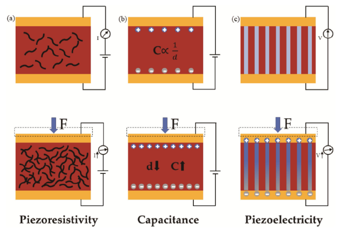
According to working principles, flexible pressure sensors can be divided into piezoresistivity, capacitance, piezoelectricity (Fig.2), or other working mechanism, for example, triboelectricity. Piezoresistive and capacitive flexible pressure sensors have been widely studied owing to their simple working principle and easy fabrication process. Numerous studies have been carried out on piezoresistive and capacitive flexible pressure sensors, and high-performance flexible pressure sensors are often designed, especially high-sensitivity. In Sections 3 and 4 of this review, piezoresistive and capacitive flexible pressure sensors with high sensitivity are discussed in more detail.
Fig. 2. Schematic illustrations of three common transduction methods: (a) piezoresistivity, (b) capacitance, and (c) piezoelectricity.
The working principle of a piezoresistive flexible pressure sensor is based on the change of pressure applied from the outside, which is reflected as a change in the corresponding resistance value. Piezoresistive flexible pressure sensors have been widely studied and applied owing to their simple structure and working mechanism, relatively simple fabrication process, and excellent performance. Therefore, extensive research has been carried out to obtain flexible pressure sensors with excellent performance.
Compared to traditional piezoresistive pressure sensors, piezoresistive flexible pressure sensors need both flexibility and a pressure sensing function. Studies on piezoresistive flexible pressure sensors typically focus on the selection of flexible materials as the most common method of achieving flexibility. Flexible pressure sensors based on this implementation usually consist of two flexible electrodes with a micro to nano-scale structures. At the same time, researchers have proposed several other methods for improving the performance of pressure sensors, especially sensitivity. The use of materials with excellent properties like carbon nanotubes and graphene as an electrode material, and flexible substrates with unique microstructures is reported. In addition, structural design for achieving flexibility and stretchability is common in the study of flexible electronic devices, but reports on the structural design of flexible pressure sensors are relatively rare. To summarize, piezoresistive flexible pressure sensor designs can be divided into three types: fabricating of microstructured flexible substrates by mold, fabricating of elastic porous conductive materials, and other designs.
Common substrates used in flexible electronic devices include PDMS, polyethylene terephthalate (PET), polyimide (PI), and polyethylene naphthalate (PEN). Among these, PDMS is a colorless, transparent, elastic polymer with stable physical and chemical properties that is widely used in flexible pressure sensors. Micro-structured PDMS is commonly used as a substrate and combined with carbon nanotubes, graphene, or some other conductive material as the electrode. This basic approach can be used to fabricate piezoresistive flexible pressure sensors. Uncured PDMS is a transparent colloidal liquid, the PDMS is first spin-coated onto a micro-structured mold, heat-cured, and then peeled off to obtain the final micro-structured substrate. Microstructures create air gaps between the electrodes and when the two electrodes are pressed together, the contact area increases and sensitivity of the sensor improves.
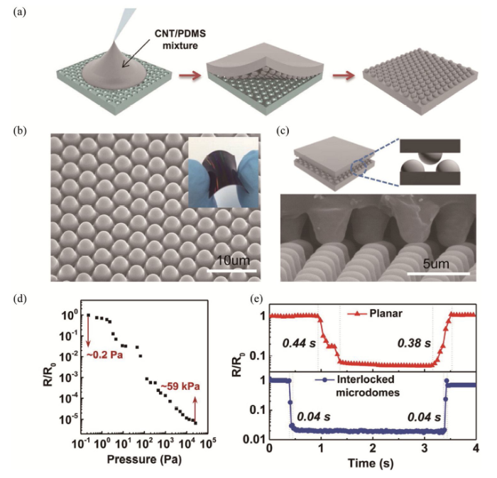
Ko et al. [27] used a silicon mold with periodic spherical holes to cast a mixture of carbon nanotubes and PDMS. After heating and curing, a conductive PDMS film with spherical microstructures was obtained (Fig. 3 (a-c)). Conductive films with spherical microstructures can also be prepared and two identical films are placed side by side to assemble the device and the resulting pressure sensor demonstrated high sensitivity of up to 15.1 kPa-1 and a minimum pressure of 0.2 Pa can be detected with a response time of only 0.04 s (Fig. 3(d and e)). Microcone arrays are another classical microstructure used for micro-structured PDMS films [28].
Fig. 3. (a) Procedure for fabricating microdome arrays; (b, c) SEM images of microdome arrays; (d) Pressure-response curve for an interlocked microdome array (8 wt % CNTs) with a minimum detection limit of ∼0.2 Pa; (e) Response/relaxation curve. Reproduced with permission [
Technologies such as photolithography and etching can also be used to obtain rigid microstructured silicon molds. These microstructured films can be combined with electrode materials such as carbon nanotubes and graphene to obtain sensors with high sensitivity [[29], [30], [31], [32], [33]]. In this way, Ha et al. [34] used photolithography to fabricate micropores of a certain depth on silicon wafers, and then poured PDMS on the module to obtain the films with cylindrical microstructures, and the final sensor offered a sensitivity of 2.0 kPa-1 in the pressure range below 0.22 kPa-1. However, these methods also have some shortcomings.
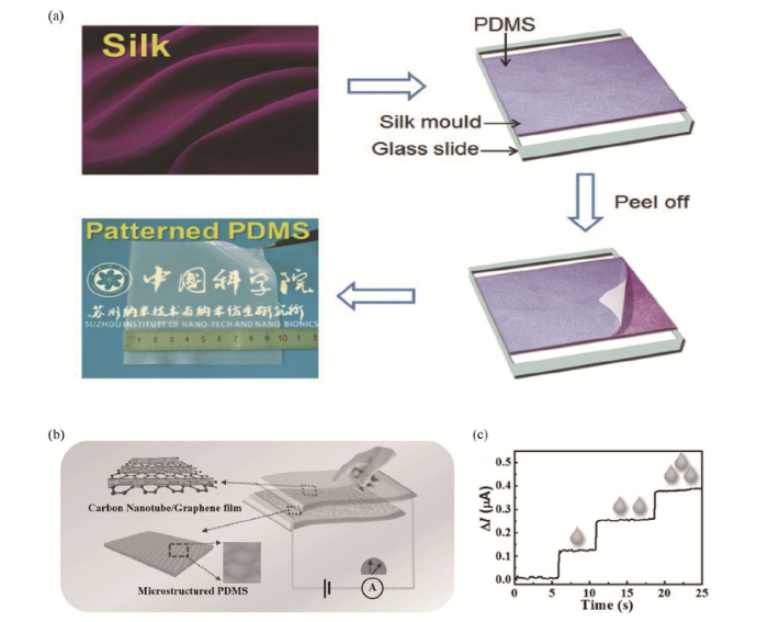
Although microstructured PDMS films fabricated using microstructured silicon molds can create highly sensitive pressure sensors and high-performance devices, fabrication costs are relatively high owing to the mold requirements, photolithography process, and other aspects of the process. Therefore, researchers have, instead, turned their attention towards nature. Zhang et al. [35] used the silk as a mold to obtain an ultra-sensitive pressure sensor. Silk is made up of silk and silk, and the pattern is dense and regular. The silk was fixed on glass, then PDMS was poured on top and heat-cured to obtain micro-structured films with a dense and regular silk pattern (Fig. 4(a)). Next, carbon nanotube films were transferred onto the micro-structured surface to obtain conductive films with a silk microstructure. Sensors fabricated using this method exhibit high performance and with a sensitivity of 1.8 kPa-1, can detect weak pressures of around 0.6 Pa with a response time of less than 10 ms and high stability. Moreover, the sensors are cheaper to fabricate compared to silicon molds and enable the preparation of large electronic skins. Apart from textiles such as silk, biomimetic structures have been investigated for preparing microstructured PDMS films [36,37]. For example, Zhang et al. [38] used the natural leaf pattern as molds for obtain microstructured PDMS films, and fabricated composite films of carbon nanotubes with graphene as the electrode (Fig. 4(b and c)). The prepared sensors offer excellent performance and can work at an ultra-low voltage of around 0.03 V.
Fig. 4. (a) Schematic illustration of fabrication process for flexible patterned PDMS films. Reproduced with permission [
Structural designs such as cracks, interlocks and wrinkles can make sensors more stretchable [[39], [40], [41], [42]]. Inspired by crack-shaped slit organs of spiders, Choi et al. designed a multifunctional sensor based on nanoscale crack junctions (a ‘nanoscale crack sensor’) and demonstrated its ultrahigh sensitivity to physiological signals (speech patterns and heart rates) and external forces (pressure, strain and vibration) [12]. And the device is durable and mechanically flexible. Inspired by the hair interlocking structure, Suh et al. [43] produced a flexible pressure sensors with platinum-coated nanofibers that not only detect pressure, but also torsion and shear.
Nanopillars are commonly fabricated using self-assembled polystyrene microspheres and other structures as a template. Recently, researchers used this type of mold to fabricate microstructured PDMS films for highly sensitive pressure sensors [44]. Wong et al. laid a single layer of polystyrene microsphere arrays on a glass substrate, then poured PDMS on the surface of the substrate, which was then heated and solidified, and finally, the polystyrene microspheres chemically dissolved leaving the microstructured substrate. The method can be used to obtain PDMS films with microsphere structures and has been used to prepare flexible pressure sensors with gold as the electrode, presenting a much simpler and cheaper method of preparing microstructures in contrast to the expensive photolithography process [45].
Elastic porous conductive materials are also widely used in piezoresistive flexible pressure sensors. Owing to the presence of pores, the material is more easily compressed and compared to microstructured PDMS films, the materials have a larger pressing range. Moreover, the fabrication process is simpler and less expensive. Bao et al. [46] invented flexible pressure sensors based on an elastic microstructured conductive polymer. Elastic microstructured films are made of a polypyrrole conductive hydrogel with hollow spherical microstructures and create pressure sensors with high sensitivity of up to 133.1 kPa-1. Preparation of porous conductive materials by combining porous microstructured PDMS with carbon nanotubes has also been reported [47].
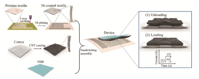
Textiles are everywhere in our daily lives. Compared to airtight PDMS films, comfortable and breathable textiles are better suited for the fabrication of flexible pressure sensors, and pores and textures of the fabric provide excellent microstructures. Flexible pressure sensors with excellent performance can be obtained by combining textiles with conductive materials such as carbon nanotubes to prepare hybrid conductive materials. One advantage is the ability to produce sensors with large areas, which is not always possible with other materials. Wang et al. prepared a device with a sensor consisting of two parts (Fig. 5): conductive cotton on top, obtained by immersing cotton in a single-walled carbon nanotube solution; fabric coated with Ni on the bottom [16]. The elasticity and microstructure of the fabric creates a sensor with excellent performance with a high sensitivity of 14.4 kPa-1, a low detection limit of 2 Pa, fast response time of 24 ms, and low power consumption (<6 μW). Fabrics like nylon are also used to fabricate flexible pressure sensors [48].
Fig. 5. Schematic illustration of fabrication process of textile pressure sensors. Reproduced with permission [
Most studies on flexible sensors focus on increasing the flexibility and sensitivity of the sensor and studies on textile-based flexible pressure sensors are no exception. However, stability and reliability are also important factors to consider for electronic skins and wearable devices. Textile-based sensors can detect physiological information during sleep. However, ensuring the sensor is not damaged when the fabric is washed is an important aspect that must be considered in the design process. Takei et al. [49] designed a textile-based pressure sensor that solves all of the above problems. The washable sensors are highly reliable with good repeatability (≈250,000 cycles, ≈5 kPa).
The two-dimensional layered material, MXene, has excellent electrical conductivity, but is rarely combined with insulating, elastic porous materials. Yu et al. [13] used MXene nanosheets and thin paper with a porous structure to obtain a sensing device with superior performance. The device is made of a thin paper and other biodegradable materials, and is therefore, extremely environmentally friendly. The use of carbon materials, metal nanomaterials, etc., is more common, and the combination of paper-based materials with metal nanomaterials, such as silver nanowires [50] or gold nanowires [51], has also been reported. In addition, traditional animal leather has been combined with different functional materials, including carbon nanotubes, to provide a new platform for multi-functional electronic skins [52].
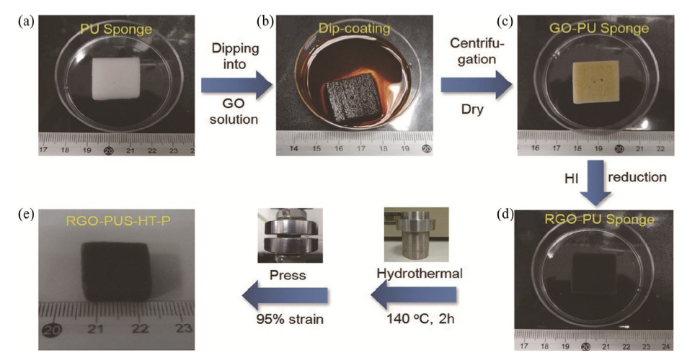
Conductive porous sponges with excellent electrical conductivity and mechanical flexibility are widely used in piezoresistive flexible pressure sensors. To improve sensitivity of the pressure sensors, Yu et al. [53] created conductive sponges with fractured microstructures (Fig. 6). First, the polyurethane (PU) sponge is immersed in graphene oxide solution to obtain a reduced graphene oxide (RGO) conductive sponge, and hot hydrogen iodide reduces the graphene oxide, and the RGO-PU conductive sponge is pressed and undergoes other processes to obtain the final fractured microstructure. The sensor has high stability as well as improved sensitivity.
Fig. 6. Fabrication of graphene-wrapped polyurethane (PU) sponge with fractured microstructure: (a-e) Schematic of fabrication process. Reproduced with permission [
Similarly, traditional pressure-sensitive rubber (PSR) has poor sensitivity, but introducing a porous structure can effectively increase the shape variable of the rubber and improve the sensitivity of rubber-based sensors [54]. Two-dimensional MXene has a wide interlayer distance and can be used to fabricate high-sensitivity pressure sensors [55]. Numerous reports have been published on immersing sponges, foams, etc. in graphene oxide solutions, followed by other processing steps to obtain elastic conductive materials [[56], [57], [58]]. Qu et al. [59] reported an ultra-sensitive pressure sensor based on foamed graphene blocks. Sensitivity of the sensor is as high as 229.8 kPa-1 and extremely small pressures such those produced by the weight of dandelion flowers, feathers, and hair can be detected. Graphene foams produce by 3D printing have also been reported [60]. Furthermore wearable sensors based on silk carbonization [61] and three-dimensional (3D) conductive films [62], and so on exist.
Without a doubt, flexible pressure sensors with high sensitivity are the primary aim and a lot of research has been carried out with this goal in mind, including studies on microstructure design, porous elastic materials, and so forth. However, pressure sensors with only high sensitivity are not ideal since stability, power consumption, resolution, etc. should also be considered. Generally, the electrode of piezoresistive flexible pressure sensors is always switched on, even in the initial state, producing a contact resistance. Power consumption under standby conditions is wasteful but can be reduced if the electrodes are designed to be non-conducting in the initial state.
In this way, Tang et al. [63] reported an energy-saving piezoresistive flexible pressure sensor composed of a sandwich structure: identical upper and lower parts comprised of a layer of wrinkled graphene on a PDMS surface and a porous anodized aluminum film in the middle. When no pressure is applied, the porous anodized aluminum film separates the upper and lower layers of wrinkled graphene, and no current flows; when pressure is applied, current flows because the two graphene layers is conducted through pores of the film. Since no current is generated when no pressure is applied, energy is saved. At the same time, the sensor offers high sensitivity. The electrode material is comprised of carbon nanotube films and the isolation layer is SU8 photoresist with a microporous structure. Microvia were obtained by a conventional photolithography technique. In another study, Gui et al. [64] reported a similar pressure sensor design.
Many large-area pressure sensor arrays have been fabricated by combining flexible pressure sensors with field effect transistors (FETs). Compared to the piezoresistive flexible pressure sensors introduced earlier in this paper, pressure sensors based on field effect transistors have a clear advantage in terms of resolution. These high-resolution devices can be applied in fingerprint recognition and similar applications. Moreover, FET-based devices are more integrated than other combined devices. Pressure sensing is achieved by connecting a varistor to the source/drain electrode of the field effect transistors [65,14]. In earlier research, Someya et al. [66] reported a large-area flexible pressure sensor matrix based on organic field effect transistors. The drain of the transistor is connected to the varistor and changes in pressure alter the resistance of the load side, such that the output current varies depending on the magnitude change of pressure. Deformable source-drain electrodes have also been studied to achieve a change of contact resistance with pressure [67].
In Section 3.1, in order to improve the sensitivity of pressure sensors, researchers fabricated micro-structured flexible substrates by molds (silicon, silk, leaf, etc.). When the pressure is constant, the contact area between micro-structured substrates is larger as well as the change of resistance. Combined with the active material (graphene, carbon nanotube, etc.), the sensitivity can be improved significantly. In Section 3.2, owing to the presence of pores, elastic porous conductive materials are more easily compressed. So the change of resistance is larger when pressure is constant, and sensitivity is improved. In Section 3.3, the electrodes are designed to be non-conducting in the initial state, and power consumption can be reduced. The area can be reduced significantly by using the transistor as the sensor unit. Pressure sensors based on the field effect transistors have a clear advantage in terms of the resolution.
Capacitive flexible pressure sensors are another widely investigated type of pressure sensor and exhibit many similarities to piezoresistive sensors. Compared to pressure sensors with other working principles, capacitive flexible pressure sensors offer the advantages of faster response times and lower power consumption. The capacitance of a parallel plate capacitor can be calculated by formula (1):
C = εA /d (1)
where ε represents the dielectric constant, A is the area of overlap of the upper and lower plates, and d is the spacing between plates [68]. In theory, changing ε, A, and d can change the capacitance.
Capacitive sensors can be divided into three types: variable area, variable dielectric, and variable pole distance. To obtain a highly sensitive resistive flexible pressure sensor, researchers have increased the sensitivity by reducing the elastic resistance of the dielectric layer. The sensitivity of a capacitive sensor is defined as formula (2):
S = (ΔC / C0) / ΔP (2)
where S represents sensitivity, ΔC is the change in capacitance, C0 is the initial capacitance when no pressure is applied, and ΔP represents the applied pressure. Therefore, to improve sensitivity, the ratio ΔC/C0 must be increase when ΔP is constant. Additional studies focused on improving other performance indicators of capacitive sensors, such as the measurement range.
In terms of design, capacitive and resistive sensors have many similarities. For example, the micro-structured PDMS films used in resistive pressure sensors can also be used as the dielectric layer of capacitive sensors or alternatively, an insulating elastic material can be selected as the dielectric layer. Of course, the fabrication processes of the two sensing mechanisms will have some differences. Similar to piezoresistive pressure sensors, the research of capacitive flexible pressure sensors can be divided into three categories: sensors based on micro-structured dielectric layer and electrode, field effect transistor types, and others.
An effective method of improving the sensitivity of capacitive flexible pressure sensors is fabricating microstructured dielectric layers. The presence of microstructures increases the air gap between the two electrodes and the dielectric layer more susceptible to deformation. From the sensitivity calculation formula, capacitance of sensors with microstructures is lower than without microstructures for the same substrate thickness because the dielectric constant of air is smaller. When pressure is applied, the air gap is reduced. Thus, under the same pressure and for the same dielectric layer thickness, the sensor with microstructured dielectric layer and electrode has smaller initial capacitance and larger capacitance change, and the sensitivity is therefore higher.
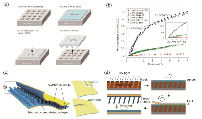
As early as 2010, Bao et al. [69] reported a capacitive flexible pressure sensor based on pyramid microstructures (Fig. 7(a and b)). The electrode of the sensor uses indium oxide (ITO) on the PET substrate and microstructured PDMS films as the dielectric layer to form a sandwich-structured device. The micro-structured mold was obtained by wet etching of silicon and liquid PDMS was poured onto the silicon to obtain a PDMS film with pyramid microstructures. The same team used finite element modeling to investigate the effect of different microstructures on reducing the effective mechanical modulus, and ultimately, found pyramid structures to be the optimal shape for reducing the effective mechanical modulus of an elastomer about an order of magnitude [70]. The presence of microstructures results in high sensitivity and fast response. Similarly, Lu et al. [71] fabricated a device with a tilted microcolumn structure (Fig. 7(c and d)). In contrast, the study did not etch silicon to obtain the mold but instead, used a 30-μm-thick photoresist with a pattern formed by photolithography. In addition, Shen et al. [11] improved the dielectric layer material by incorporating silver nanowires into polydimethylsiloxane (PDMS), and then poured the mixed liquid onto the silicon mold with pyramid microstructures. The combined micro-structured dielectric layer and silver nanowires produced a sensor with high sensitivity (0.831 kPa-1, <0.5 kPa).
Fig. 7. (a) Schematic illustration of microstructured PDMS film fabrication process; (b) Pressure-response curves for different types of microstructured PDMS films. Reproduced with permission [
In addition to the design of pyramid microstructures [72], bionics has also been incorporated into the design capacitive pressure sensors. Guo et al. [73] reported a high sensitivity (1.2 kPa-1) flexible capacitive pressure sensor with a high aspect ratio (≈2) that used a lotus leaf as a mold for obtain a PDMS film with surface microstructures. In contrast to PDMS films produced by the conventional methods as the dielectric layer, the researchers coated the surface of the PDMS film with an ultra-thin nano-silver layer to create the lotus leaf microstructure. The technique was applied to the bottom electrode of the sensor instead of the dielectric layer.
Fabricating of microstructured electrode has also been researched widely [[74], [75], [76]]. Hong et al. [77] reported a low-cost and facile fabrication strategy to obtain multiscale-structured elastomeric electrodes. The capacitive pressure sensor with the multiscale-structured elastomeric electrode shows high sensitivity (>3.8 kPa-1). Similarly, Zhang et al. [78] reported a capacitive sensor with a lotus leaf micropattern as an electrode template, and a dielectric layer of polystyrene microspheres. Compared to PDMS films without microstructure, the micropores increase the plate area when pressure is applied, and microspheres inside holes are squeezed out, both of which increase the change in capacitance change and improve sensitivity of the sensor. Inspired by micro-hair structures of skin found in nature, Bao et al. [79] reported a super-compliant capacitive sensor. The area of the sensor attached to the skin is made of PDMS with a micro-hair structure.
By combining transistors and sensors, each transistor is a sensor unit, which has the clear advantages of improving integration of the device and obtaining a high-resolution sensor. One of the major goals of flexible sensors is the development of electronic skin, however, high resolution is necessary to achieve this. Unlike field-effect transistor-based piezoresistive pressure sensors, field-effect transistor-based capacitive pressure sensors detect changes gate capacitance when pressure is applied. The drain current of the transistor is related to the gate capacitance: the larger the capacitance, the larger the output drain current.
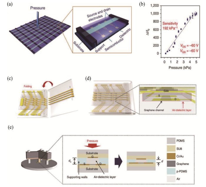
Based on a sensor comprised of pyramid micro-structured PDMS films, Bao et al. [69] used the microstructured PDMS films as an insulating layer to fabricate a top-gate transistor. The presence of the microstructured PDMS enables high sensitivity and fast response times. Further, the team implemented a flexible pressure-sensitive organic thin film transistor [80] that is 15 times more sensitive than the previously presented transistor [69]. Furthermore, Zhu et al. [81] reported a suspended gate organic thin-film transistor (SGOTFTs) with a sensitivity of up to 192 kPa-1, which has not been reported previously (Fig. 8(a,b)). The presence of a support layer creates a large air gap between the flexible floating gate and the source and drain electrodes of the transistors. The device offers high sensitivity since only a tiny pressure is needed change the gate capacitance.
Fig. 8. (a) Structure of pressure sensor device; (b) Pressure response of the source-drain current with a pressure sensitivity of up to 192 kPa-1. Reproduced with permission [
Most research on flexible pressure sensors has focused on obtaining sensors with high sensitivity. This particular performance parameter is critical, nonetheless, other parameters such as measurement range are also important. A narrow measurement range will greatly limit the range of applications. In view of this, Park et al. [82] reported an air dielectric-based transistor array for pressure sensing with an extremely large pressure sensing range (250-3 MPa) (Fig. 8(c-e)). The transistor array is composed of two plastic plates and a foldable elastic joint. The source and drain electrodes and the channel are on a single substrate, and the gate is on another. The patterned photo-patternable PDMS (p-PDMS) layer causes the two substrates to fold into a metal-air-graphene structure, and also ensures alignment of the device. Thicker p-PDMS increases the height of the air dielectric layer, which increases the measurement range. Furthermore, another group proposed a flexible low-voltage organic thin-film transistor with a new type of polyelectrolyte dielectric to achieve high-sensitivity pressure detection [83].
Microstructured dielectric layer and electrode have been fabricated to obtain high-sensitivity pressure sensors and field-effect transistor-based pressure sensing are the two main directions of study capacitive flexible pressure sensors. In addition, many reports propose the use of other dielectric materials as the dielectric layer, such as Graphene oxide(GO), air, polyurethane(PU),polymethylmethacrylate(PMMA) and so on. [76,[84], [85], [86], [87]] Bao et al. [88] presented a flexible transparent capacitive pressure sensor based on carbon nanotube films. The dielectric layer of the capacitive sensor is composed of Ecoflex, which is more susceptible to deformation than PDMS. Therefore, capacitance of the sensor changes linearly within a large pressure range. Guo et al. [89] reported a capacitive sensor that applies plant materials including leaves and petals as the dielectric layer. The dried petal or leaf is a foam-like hollow structure and can be highly compressible. So the sensor shows a high sensitivity of 1.54 kPa-1 in a low pressure range.
The use of a porous elastomer as the dielectric layer can also increase sensitivity of the sensor [[90]]. Park et al. [91] reported a flexible wearable capacitive pressure sensor based on a 3D microporous dielectric elastomer. The presence of micropores allows the sensor to be compressed more easily, resulting in higher sensitivity and a larger pressure-sensing range. Pan et al. [92] used the iontronic film for capacitive pressure sensing. Additionally, some studies have focused on designing sensors with other capabilities, such as transparency [93], easy integration with highly deformed areas [94], simultaneously detecting multiple stimuli [95], and so on. Common structures and sensitivity of resistive and capacitive pressure sensors are presented in Table 1.
Table 1 Structure and sensitivity of common resistive and capacitive pressure sensors.
| Type | Structure | Sensitivity | Reference |
|---|---|---|---|
| piezoresistivity | microdome | 15.1kPa-1 | [27] |
| piezoresistivity | micropyramid | 10.3 kPa-1 | [28] |
| piezoresistivity | micropillar | 2.0 kPa-1 | [34] |
| piezoresistivity | silk-molded | 1.80 kPa-1 | [35] |
| piezoresistivity | bionic hierarchical | 19.8 kPa-1 | [38] |
| piezoresistivity | hollow sphere | 133.1kPa-1 | [46] |
| piezoresistivity | textile | 14.4 kPa-1 | [16] |
| capacitance | pyramid | 0.55 kPa-1 | [69] |
| capacitance | lotus leaf-mold | 1.2 kPa-1 | [73] |
| capacitance | Transistor | 192 kPa-1 | [81] |
| capacitance | tilted micropillar | 0.42 kPa-1 | [71] |
| capacitance | nanoparticles | 1.0 kPa-1 | [93] |
In Section 4.1, the presence of microstructures increases the air gap between the two electrodes and the dielectric layer more susceptible to deformation. When the pressure is applied, the air gap is reduced. Thus, with the same pressure and dielectric layer thickness, the sensor with micro-structured dielectric layer has smaller initial capacitance and larger capacitance variation, therefore the sensitivity is higher. In Section 4.2, each transistor is a sensor unit, which has the clear advantages of improving the device integration and obtaining a high-resolution sensor. In Section 4.3, the dielectric layers with porous structures and low effective elastic modulus have larger capacitance variation under the same pressure, so the sensitivity is higher.
Certain dielectric materials exhibit the so-called piezoelectric effect under pressure. Piezoelectric sensors make use of this effect. The piezoelectric effect occurs when a dielectric material undergoes deformation due to external forces acting in a certain direction, such as bending or telescopic deformation. Owing to the polarization of internal charges, they will be sized on opposite surfaces of the material and emerge the opposite bound electric charge. When the external force is removed, the material returns to its uncharged state. Piezoelectric sensors have high sensitivity and fast response times to applied dynamic pressure; however, static responses are unreliable.
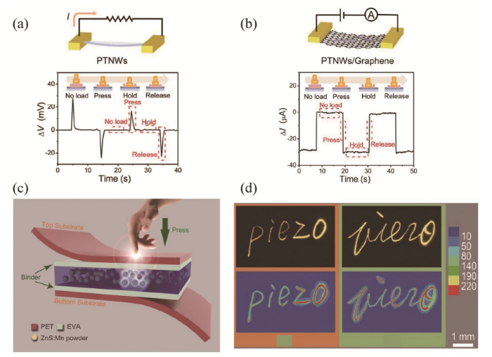
Both polymer and inorganic materials, such as ZnO, are widely used in flexible piezoelectric pressure sensors. Wang et al. [96] has performed a lot of notable work in this area. Other researchers have also studied flexible piezoelectric pressure sensors. Rogers et al. [97] used PVDF, a flexible piezoelectric material, to fabricate high-performance piezoelectric devices. Earlier reports include the use of a vertical zinc oxide nanowire-based piezoelectric transistor integrated circuit by Wang and co-workers, which can be used as a pressure sensor array for tactile imaging [98]. Further to this, Wang et al. [99] reported a pressure sensor array based on nanowire-emitting light-emitting diodes (LEDs). Sensor arrays are capable of measuring two-dimensional pressure distributions with high spatial resolution of up to 2.7 μm and a corresponding pixel density of 6350 dpi. Each pixel consists of a single n-ZnO nanowire/p-GaN light emitting diode. It takes only 90 ms to create the measured pressure map. Usually, piezoelectric pressure sensors can only be used to detect dynamic pressure and due to the piezoelectric effect, the output voltage is a pulse signal that can only be detected at the moment the sensor switches between the on and off mode. To solve this problem, Xu et al. [100] fabricated a nanowire/graphene heterojunction-based sensor with a sensitivity of 9.4 × 10⁻³ kPa-1 when the pressure is static and a response time of only 5∼7 ms (Fig.9(a,b)). In addition, the triboelectric mechanism has also been studied [101].
Fig. 9. (a) Pressure response of a pure PTNW-based pressure sensor under a pressure pulse; (b) Pressure response of a PTNWs/G transistor under a pressure pulse. Reproduced with permission [
Wang's group found that the piezopotential created in ZnO nanowires had a positive influence on the strong trapping electrons in vacancy or surface states. And it was pointed out that the strain-induced piezopotential might make these trapped charges drop to the valence band, leading to photon emission, which is also called piezophotonic effect [102]. The piezophotonic effect widely exists in many piezoelectric materials, such as transition metal doped ZnS, CaZnOS, SrAl2O4, and LiNbO3. And these materials have excellent mechanoluminescent properties. Piezophotonic effect based on mechanoluminescent materials have widely applications in flexible optoelectronic devices [[103], [104], [105]]. Wang et al. [106] reported a wafer-scale, flexible pressure sensor matrix (PSM) for securer signature collections (Fig. 9(c and d)). The implementations of these features are based on the mechanoluminescence (ML) of ZnS:Mn particles (ZMPs) for instantaneous mapping of pressure of both a single point and a 2D planar distributions ranging from 0.6 to 50 MPa through a conversion process between mechanical stress and visible light emissions. This device has a high-definition two-dimensional (2D) pressure mapping of the dynamic signing process with time response of 10 ms and spatial-resolution of less than 100 μm (254 dpi). Furthermore, this PSM device is self-powered and requires no external electric power for operations. Similarly, Song et al. [107] reported a flexible sensitive mechanoluminescence device. Different from those mechanoluminescence devices needs strong stimuli. This device can achieve weak stimuli driving.
A great deal of research has been performed on improving the performance of flexible pressure sensors, and in particular, sensitivity. In addition, many studies propose flexible pressure sensors with other capabilities, such as multi-sensing abilities, self-healing properties, and more. Flexible pressure sensors based on the above-mentioned high-performance criteria and other functions are also used as electronic skin and a flexible wearable device, and have been widely used for monitoring physiological information such as breath, pulse, and human-machine interfaces. Fig. 1 shows flexible pressure sensors and their applications in electronic skin and flexible wearable devices.
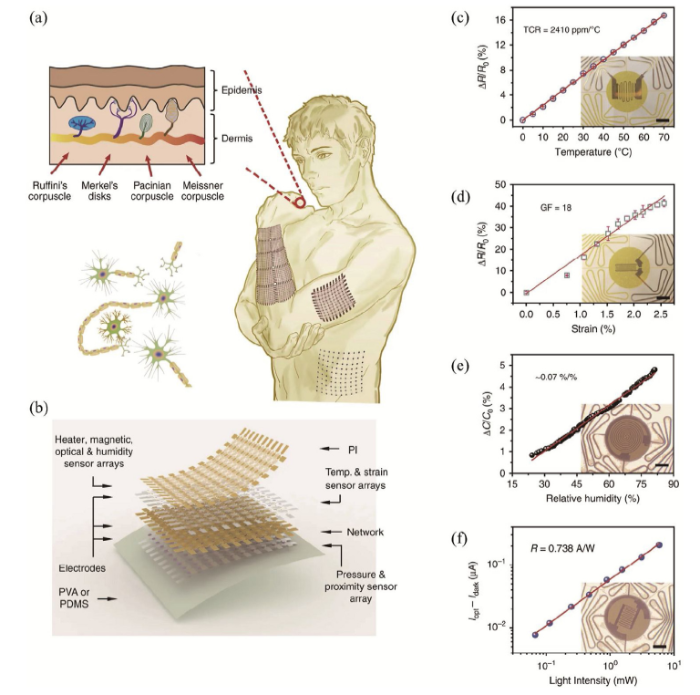
Electronic skin with multiple detection functions have been reported [[108], [109], [110]]. These electronic skins are, in fact, sensor arrays capable of detecting multiple variables, whereas pressure sensors only make up a small part of electronic skin systems. Recently, Wang et al. [111] reported a skin-inspired highly stretchable and conformable matrix network (SCMN) with high scalability and compliance. The integrated sensor arrays offer a variety of detection functions including, but not limited to, temperature, in-plane strain, humidity, light, magnetic field, pressure, and proximity, as well as simultaneous multi-stimulation sensing with an adjustable sensing range and large area, and may be suitable for high-density 3D integration solutions. Fig. 10 shows a schematic illustration of an SCMN an integrated sensor array with eight different functions.
Fig. 10. (a) Schematic illustration of skin-inspired matrix network (SCMN) conforming to the surface of a human arm; (b) An integrated sensor array with eight functions; (c) Temperature sensing, (d) strain sensing, (e) humidity sensing, (f) light intensity detection. Reproduced with permission [
Self-healing is an important property of electronic skin. The skin of humans and other organisms constantly self-renews. When skin is damaged, it can repair itself. Therefore, developing a flexible pressure sensor with self-healing capabilities would be extremely meaningful in terms of practical applications such as robotic skin. Two strategies are typically used to achieve self-healing function of materials: loading the material with self-healing properties; providing energy in the form of heat, illumination, etc., to trigger crystallization, film formation, or cross-linking and thus, “self-healing” effects [3]. In recent years, there have been many reports on electronic skin composed of materials with self-healing capabilities [112,113]. Tee et al. [114] introduced a transparent conductive self-healing material in a dry or humid environment that can be used as a flexible pressure sensor or strain sensor that has demonstrated considerable potential in the field of electronic skin.
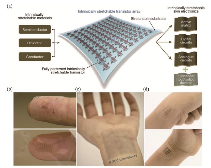
Flexible pressure sensors are used in electronic skin systems and flexible wearable devices to make them stretchable. Stretchability of the flexible pressure sensors enables the device to bond better to non-planar surfaces and protects sensors from damage due to continuous deformation. In general, stretchability is achieved in two ways: developing stretchable materials; structured design [1]. Both strain sensors and flexible sensors with stress and strain detection capabilities have been reported. As shown in Fig. 11, Bao et al. [15] reported a fabrication process for creating a fully stretchable transistor array, not previously repored. The intrinsically stretchable transistor array consists of stretchable material and is capable of accurately detecting the position of ladybug feet, thereby achieving high-resolution touch perception.
Fig. 11. (a) Intrinsically stretchable transistor array; (b) An array of 108 stretchable transistors on a fingertip; (c) 6300 transistors in an area of around 4.4 × 4.4 cm2; (d) Electronic skin conforms perfectly to skin. Reproduced with permission [
In this review, we introduced flexible pressure sensors, both piezoresistive and capacitance, from the perspective of improving the primary performance index, sensitivity. To obtain highly sensitive pressure sensors, researchers have proposed a number of designs involving various microstructures and porous elastic materials. Many researchers are now moving in the direction of electronic skin with multiple functions, self-healing properties, and other capabilities, enabled by high-performance pressure sensors.
The true meaning of "skin" is a complete system that combines multiple detection functions, self-healing and self-powering abilities, biocompatibility, and biodegradability. Wearable devices do not necessarily need to function like human skin, but should be capable of performing required functions and should also have a suitable power source. The development of large-area flexible pressure sensors is another important area of research, and could be particularly relevant to patients with large skin burns requiring skin grafts or robotic skin. Most pressure sensors are sandwich-like structures that create a sensor array with low resolution and are not suitable for high-resolution applications such as precision fingerprinting. Although FET-based sensor arrays have higher resolution, their stretchability is poor. Recent reports of fully stretchable transistors may offer potential solutions to this problem.
A sensor is a detection device that senses information from the external environment and transforms data into an electrical signal or another desired form of output according to certain rules. The detected signal must be processed by a subsequent circuit (such as analog signal to digital signal conversion) to meet demands of the particular application. In addition, signal transmission systems (such as wireless transmission technology), stability of the device, and the cost of fabricating electronic skin and flexible wearable devices are all problems that need to be solved to transition from the laboratory to daily life. Sensor technologies are the key to realizing the IoT, and only by solving these problems can we truly enter a fully interconnected era.
This work is supported by the National Natural Science Foundation of China (Nos.61775032, 61475134 and 11604042), the Fundamental Research Funds for the Central Universities (N170405007, N180406002, N180408018 and N160404009), and the 111 Project (B16009).

 WeChat
/
| 〈 |
|
〉 |