Search for articles:
Ji-Ye Baek
Corresponding authors:
Received: 2019-07-15
Revised: 2019-09-22
Accepted: 2019-10-27
Online: 2020-04-01
Copyright: 2020 Editorial board of Journal of Materials Science & Technology Copyright reserved, Editorial board of Journal of Materials Science & Technology
More
Abstract
An ultrathin SrTiO3 dielectric layer is optimized through Al doping to solve the problems existing in development of ultra-high-k oxide MOS capacitors. Through post-deposition annealing, Al doping induces changes in the electronic structure of SrTiO3, thereby effectively reducing leakage current to <10-8 A/cm2 at 0.5 MV/cm but maintains good capacitance values (ε > 80) of ultrathin SrTiO3 MOS capacitors.
Strontium titanate (SrTiO3) is a high-k material but its bandgap is smaller than that of other oxide dielectrics (e.g., SiO2, Al2O3). Consequently, an ultrathin SrTiO3 film may have a high tunneling leakage current, which is not suitable for capacitor-based applications. To improve the performance of metal-oxide-semiconductor (MOS) capacitors using SrTiO3, an approach based on homogenous and uniform aluminum doping to SrTiO3 through co-sputtering is introduced. The bandgap of a pristine SrTiO3 film showed an increase of 0.5 eV after Al doping. Furthermore, Al doping decreased the leakage current of SrTiO3/Si-based MOS capacitors by more than five orders of magnitude (at the level of nanoampere per square centimeter). Importantly, a dielectric constant of 81.3 and equivalent oxide thickness less than 5 Å were achieved in an 8-nm-thick Al-doped SrTiO3 film owing to changes in its crystal structure and conduction band edge electronic structure. Thus, the obtained data show the effectiveness of the proposed approach for solving the problems existing in the development of ultra-high-k oxide MOS capacitors.
Keywords:
So far, the development of integrated circuits has involved an increase in the density of transistors by reducing their size in order to incorporate more transistors into a limited area. As devices become finer, the thickness of the gate insulator becomes extremely thin, resulting in a sudden increase in gate leakage current owing to the quantum mechanical tunneling phenomenon. Therefore, researchers have focused on developing and scaling-down oxide thin films having a high dielectric constant (k) and suppressing the tunneling effect, which are commonly achieved in thick films. [1,2]
Strontium titanate (SrTiO3 or STO) is a perovskite-type high-k oxide. Bulk STO has a theoretical k value of 300 owing to the high ionic polarizability of Ti4+ ions, which travel a large distance within the TiO6 octahedra of the cubic crystal structure of SrTiO3. Furthermore, the k value of ternary metal oxides such as SrTiO3 is several times higher than that of binary metal oxides. [3] Moreover, SrTiO3 has good thermal stability. Therefore, it can maintain a high capacitance performance over a wide temperature range, including at room temperature. [4] Consequently, SrTiO3 is a candidate for not only high-performance capacitors but also insulators for dynamic random-access memory (DRAM) applications—specifically for metal-insulator-metal (MIM) charge storage capacitor applications. Here, DRAM is an integrated circuit containing thousands of cells; each cell consists of a transistor and a capacitor. To improve device performance and accelerate signal processing, more cells must be added into DRAM with an aggressively reduced MIM capacitor but it is necessary to prevent leakage current effectively and secure the capacitance of the insulating layers owing to cell miniaturization as mentioned above. Based on an international technology roadmap for semiconductors, the future requirements of a DRAM MIM capacitor are ultralow leakage current density (10-7 A/cm2 at the operating voltage) and a small equivalent oxide thickness (EOT) <0.5 nm at a small physical thickness <5 nm. [5] To fulfill these challenging requirements, it is necessary to replace the insulator with a higher-k dielectric such as SrTiO3 or current dielectrics such as a ZrO2-Al2O3-ZrO2 layer. However, SrTiO3 has critical disadvantages for DRAM applications at nanoscale as it exhibits an intolerable tunneling leakage current.
As in the case of DRAM, a gate dielectric with higher k than that of HfO2, which is currently used in the gate stack in metal-oxide-semiconductor (MOS) field-effect transistors for integrated circuits, is favorable for the improvement of driving current at a low operating voltage. However, this is challenging as the bandgap of a dielectric inversely scales with its k value, and thus, implementation of an ultra-high-k dielectric significantly reduces the conduction band offset between Si and gate dielectric conduction band edges, resulting in an exponential increase in the tunneling-induced gate leakage current; this physical rule imposes several critical issues upon the implementation of SrTiO3 as a MOS gate dielectric. SrTiO3 has an indirect band gap of 3.25 eV and a direct band gap of 3.75 eV. At the interface of SrTiO3/Si, conduction band offset is nearly zero for the application of a MOS capacitor, and thus, a large and intolerable leakage current is induced. [6] Furthermore, the crystallinity of perovskite-type materials decreases with a decrease in the physical thickness [7]. Thus, the above issues lead to a significant decrease in the dielectric constant and an increase in the leakage current of ultrathin SrTiO3 dielectric layers. To overcome the aforementioned issues, more research and technique to improve the band gap and crystallization of SrTiO3 must be studied further. [8]
From the viewpoint of material property, most properties of SrTiO3 are attributed to its electronic structure (i.e., that of the d0 transition metal oxide). In the structure of TiO6 octahedron, Ti can travel a large distance from the center of a cubic crystal unit. This relocation causes an ultra-high k value but also a low bandgap owing to the influence of Ti 3d orbital. [9] Furthermore, a BO6 structure can be modified with a change in the size of B (i.e., cations) and the distortion of the crystal symmetry. This is the key concept for improving the electronic structure and electrical characteristics of this material. Studies have been conducted to increase the conduction band offset between SrTiO3 and a semiconductor (active channel, such as Si) to reduce leakage current. Some methods have been developed for this purpose, such as inserting high-band-offset buffer layers, [10,11] adjusting the interface oxygen stoichiometry [12,13], and adjusting the doping level to twist the BO6 structure. In the case of inserting buffer layers, the thickness of the buffer layer can affect the total capacitance of capacitors and the field effect of transistors, leading to more device-to device variation. [14] In regard to adjusting the interface oxygen stoichiometry, it is difficult to control the stoichiometry as well as the structures and electrical properties of these materials quantitatively [15]. For doping, the electronic structure of SrTiO3 is changed in this study because it is an effective method for doping ultrathin films without causing damage to other materials present on samples. In this regard, co-sputtering using radio frequency (RF) magnetron sputtering allows uniform doping and easy control of the doping amount, and is advantageous for application to actual industrial processes. [16] Particularly, RF magnetron sputtering can produce highly crystalline SrTiO3 layers at an early stage whereas atomic layer deposition (ALD) may form amorphous or defective layers owing to a nonequivalent mixture of introduced Ti and Sr precursors and residual precursors. [17,18] Furthermore, co-sputtering allows uniform and controllable doping, rendering it suitable to application in actual industrial processes.
As well known, the bandgap of SrTiO3 can be adjusted by changing the orbital energy level of ions. Since the orbital energy level is determined by the type of elements, an element having an orbital higher than the Ti 3d orbital is required to increase the bandgap. Here, our choice is the substitution of Ti with Al, which can increase the conduction band offset because the energy level of Al4s is higher than that of Ti3d. However, Ti is essential for maintaining a high k value owing to the high travel distance of Ti as mentioned above. Hence, the replacement of Ti with Al will lead to a decrease in the k value of the doped SrTiO3 [19]. Consequently, our target is to control the concentration of Ti in Al-doped SrTiO3 to optimize the balance between increasing the band gap and reduction in the k values. Co-sputtering (Al and SrTiO3 targets) was utilized in this regard to control Al doping and the thickness of SrTiO3. The crystal structure and bandgap of the materials were further explored for MOS capacitor applications. Although Al-doped STO has been applied to MIM capacitor [20], there was no report about Al-STO utilization as gate dielectric to Si MOS capacitor because of low conduction band offset and highly defective transitional interface silicate. Therefore, these findings paved the way for developing nanoscale MOS gate capacitors using SrTiO3, an ultra-high-k MOS gate oxide.
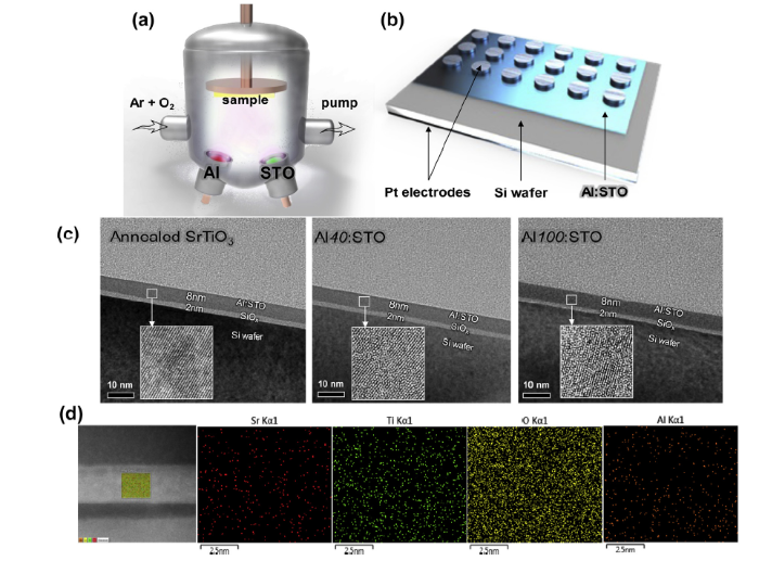
The MOS capacitors were fabricated on p-type Si substrates as demonstrated in Fig. 1. First, the wafer was prepared using modified RCA cleaning. The rear side of the wafer was then coated with a 100-nm-thick Pt layer as a bottom electrode using an electron beam evaporator (UEE, ULTEC). Subsequently, the dielectric layer of Al-doped SrTiO3 was deposited on the cleaned wafer using co-sputtering method, which facilitates the control of doping and composition. Here, an RF magnetron sputter was used with an Al target on the left side and a SrTiO3 target on the right side as shown in Fig. 1(a). The sputtering power of SrTiO3 was fixed at 100 W, and that of Al was varied to control the doping amount of Al (0, 20, 40, 60, 80, and 100 W). The working pressure was 10 mTorr with the mixture ratio of Ar:O2 = 40:10 (in sccm). The samples were heated to 600 °C before the deposition of the SrTiO3 thin film. To crystallize the SrTiO3 films, a rapid thermal annealing (RTA) system was used for PDA in an oxygen atmosphere (∼100 Torr). The post-annealing temperature and time were varied (700-850 °C and 5-60 min, respectively) to optimize the SrTiO3 crystallization. Finally, Pt as a top gate electrode was deposited using the electron beam evaporator through a hole-array shadow mask. The thickness and radius of the top Pt electrodes in Fig. 1(b) were 50 nm and 100 μm, respectively. After electrode deposition, a forming gas annealing process was performed for 30 min using the same RTA equipment to minimize interfacial defects between Pt and Al-doped SrTiO3. The process temperature was 400 °C in a reducing environment of 5% H2 in N2 gas (pressure of 0.1 Torr).
Fig. 1. Schematic diagrams of (a) co-sputtering Al and SrTiO3 via RF magnetron sputtering and (b) MOS capacitor structure with top and bottom Pt electrodes, Al-doped SrTiO3 insulator, and Si semiconductor. (c) TEM images of SrTiO3 and Al-doped SrTiO3 (sp = 40 and 100 W); inset images are captured at a magnification of 600,000 times. (d) TEM-EDS elemental mapping image of Al40:STO layer.
The structural information of Al-doped SrTiO3 thin films was investigated using X-ray diffraction (XRD, Rigaku Ultima III), field emission scanning electron microscopy (FE-SEM, Hitachi S-4800), and atomic force microscopy (AFM, PSIA XE150). The electrical properties of these capacitive films were analyzed from current density-voltage (J-V) and capacitance-voltage (C-V) characterizations using a probe station (Keithley 4200-SCS). Their capacitance maximum, flat band voltage (Vfb), and threshold voltage (Vth) were obtained from C-V curves in order to calculate their dielectric constant, EOT, and trapped charges at the oxide interface. The correlation of Al doping amount with Al sputtering power was examined through Auger electron spectroscopy (AES, PHI 700Xi) and transmission electron microscopy (TEM, JEM-2100 F, Cs corrector). The shift of electrical bandgap was measured using spectroscopic ellipsometry (VASE model; J.A. Woollam Co.). X-ray photoelectron spectroscopy (XPS, Thermo Fisher Scientific Co., Theta probe, using Al Kα (1486.6 eV) and helium (I) UV radiations) was used for identifying changes in the chemical bonding states of each constituent element as the Al doping amount increased. Also, secondary ion mass spectrometry, SIMS analysis for interfacial analysis was added.
Fig. 1(a and b) demonstrates the co-sputtering method and the device structure of capacitors based on Al-doped SrTiO3, respectively. The primary focus of this study is the control of Al doping concentration by adjusting the sputtering power for the Al target. The ratio of sputtering power for the Al and SrTiO3 targets was varied from 0:100 to 100:100 corresponding to the increase in the Al sputtering power in the order of 0, 20, 40, 60, 80, and 100 W. For convenience, the Al-doped SrTiO3 samples are denoted as Alsp:STO where sp is the Al sputtering power (W).
Fig. 1(c) shows TEM images of SrTiO3 and Al:STO layers (sp = 40 and 100 W) on Si substrates. An ultrathin SiOx layer (∼2 nm thick) was formed during sputtering; it is a mixed oxide layer with Sr, Ti, and Al cations. More interestingly, the physical thickness of SrTiO3 of all the samples is approximately 8 nm, which was used for calculating their capacitance density and dielectric constant. A similar phenomenon was observed with SrTiO3 and Al:STO samples deposited for longer periods (20-120 min) as shown in Fig. S1 (Supporting Information, SI). Their similar thickness is probably due to the higher elastic properties of Al (120 GPa) against argon bombardment than those of cubic SrTiO3 (6-14 GPa). [21] Consequently, it was confirmed through TEM with EDS measurement that the amount of Al in the Al:STO layers was small. The EDS data of Al:STO samples (sp = 40 and 100 W) are presented in Fig. S2 (SI). Fig. 1(d) shows the result of elemental mapping analysis of Al40:STO in which Al doping is uniform. Here, the average atomic percentages of Al with sp = 40 and 100 W are 5.33% and 10.26%, respectively. For confirmation, AES measurements were obtained as shown in Fig. 5(a-c). From Table 1, it can be verified that the atomic percentage of Al doped into Al40: STO and Al100:STO layers was approximately 5% and 10%, respectively.
Table 1 Atomic percentage of Al in STO layers.
| Sputtering power (W) | Al content (%) | |
|---|---|---|
| TEM-EDS | AES | |
| 40 | 5.33 | 4.8 |
| 100 | 10.26 | 9.5 |
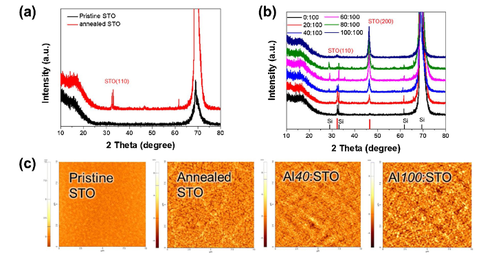
Interestingly, despite the similar thickness of SrTiO3 and Al:STO samples, there was a difference in their crystallinity, as shown in the inset images of Fig. 1(c). XRD and AFM measurements were obtained for exploring this difference. Fig. 2 (a) shows the XRD result of a pristine SrTiO3 layer. After post-deposition annealing (PDA), the layer was crystallized well, showing a peak at 2θ = 32.4° corresponding to the plane (110) of SrTiO3 (JCPDS card no. 05-0634). Al doping significantly changed the crystal orientation of SrTiO3 as shown in Fig. 2(b). Here, all the Al:STO samples had undergone post annealing at 750 °C for 30 min under oxygen conditions before XRD measurements. With sp = 20 W, a peak at 2θ = 46.5° appeared, which corresponds to the crystal plane (200) of SrTiO3. The intensity of the (200) peak increased for higher Al sputtering power whereas that of the (110) peak decreased. With sp = 100 W, SrTiO3 was almost grown only in the (200) direction. Owing to the change in crystal orientation caused by Al doping, the morphology of SrTiO3 and Al:STO layers was different as shown in Fig. 2(c). The roughness values obtained from the AFM images were 0.29, 1.17, 1.18, and 1.57 for as-deposited SrTiO3, annealed SrTiO3, Al40:STO, and Al100:STO, respectively. It was observed that the surface roughness increased with an increase in the crystallinity of SrTiO3 after annealing and Al doping. However, the layer surface was damaged, and the uniformity was lowered when sp increased (≥ 40 W). This could cause a higher leakage current in the capacitor.
Fig. 2. (a) XRD result of pristine SrTiO3: as-deposited and after PDA. (b) XRD patterns of annealed Al:STO samples (sp = 0, 20, 40, 60, 80, and 100 W). (c) AFM image of SrTiO3 layers (before and after PDA and Al:STO layers (sp = 40 and 100 W)).
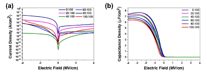
To understand the electrical properties of SrTiO3 layers with Al doping, J-V and C-V measurements were carried out as shown in Fig. 3(a and b). To obtain the current density values of the MOS capacitors based on SrTiO3 and Al:STO, reverse and forward bias voltages were applied to the Pt electrodes (see Fig. 1 (b)). In Fig. 3(a), the leakage current of the annealed SrTiO3 layer was very high (∼10-2 A/cm2) and it was significantly improved by Al doping. However, the leakage current did not decrease in proportion to the Al sputtering power or Al doping amount. The sample with the Al40:STO layer shows the greatest decrease in leakage by approximately five orders of magnitude at -1 MV/cm and four orders of magnitude at 1 MV/cm compared with that of SrTiO3. In Fig. 3(b), C-V hysteresis curves were obtained to determine the capacitance values by applying a sweeping voltage to the top Pt electrode (gate) at a high frequency of 1 MHz. Fig. S5 (SI) presents the capacitance values, which show an insignificant variation for different frequencies (10 kHz - 1 MHz). At 1 MHz, the maximum capacitance density of the annealed SrTiO3 sample was determined to be approximately 7.67 μF/cm2. As Al doping increased, the capacitance density of SrTiO3 decreased to ∼ 1 μF/cm2. Furthermore, shifts of its flat band voltage (VFB) in the negative direction with Al doping were observed. However, these shifts and capacitance decreases of Al:STO were not in a directly proportional relationship with the Al doping amount (Table S1 (SI)).
Fig. 3. (a) J-V curves of MOS capacitors with Al:STO layers (sp = 0-100 W) of thickness 8 nm. (b) C-V curves of these samples.
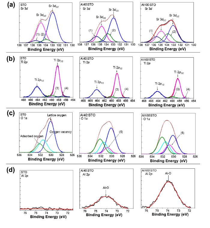
XPS was used to observe changes in the composition and binding states of SrTiO3 with and without Al doping (sp = 40 and 100 W) for determining the reason for such nonlinear relationships with Al doping levels. The core energy levels of SrTiO3 and Al:STO, such as Sr 3d, Ti 2p, O 1s, and Al 2p, are presented in Fig. 4(a-d), respectively. The Sr 3d spectrum of the SrTiO3 sample (Fig. 4(a)) showed two main peaks of Sr 3d5/2 and Sr 3d3/2 components at 132.9 and 134.7 eV, respectively. They are attributed to the bonds of Sr atoms in the perovskite structure of SrTiO3. There are two other minor peaks at 133.8 and 135.5 eV, which originate from Sr atoms in non-perovskite structure areas of the SrTiO3 film, such as Sr-OH, Sr-CO3, Sr-Sr, and Sr-O bonds at the surface. [[22], [23], [24], [25], [26], [27]] In Fig. 4(b), two major binding components of Ti4+ in the perovskite structure SrTiO3 are observed, which are Ti 2p3/2 and Ti 2p1/2 at 458.5 and 464.2 eV, respectively. There were two small peaks at 460.0 and 456.5 eV corresponding to the presence of Ti-OOH and reduced Ti-O (Ti3+), respectively. [[28], [29], [30], [31], [32], [33]] In general, the SrTiO3 structure after PDA still had some defects. The major defects could be oxygen vacancy, which is shown in the O 1s spectrum (Fig. 4(c)). As shown in this figure, the intensity of the oxygen vacancy peak (at 321.6 eV) is the second highest and is equal to ∼28% of intensity of the main peak of lattice oxygen (at 530.1 eV). The lattice oxygen peak is attributed to the Sr-O and Ti-O bonds in the perovskite structures of SrTiO3. [[34], [35], [36], [37]] Regarding Al:STO samples, with an increase in the Al doping amount, the peak intensity of Al-O bonds at 73.6 eV in Fig. 4(d) and at 530.8 eV in Fig. 4(c) increased whereas the main peaks of Sr 3d, Ti 2p, and O 1s spectra decreased. [38,39] Thus, it is confirmed that Al atoms led to the change in the crystallization of SrTiO3 as shown in Fig. 2(b). Moreover, the changes in the peak intensity in Fig. 4(a,b) suggest a replacement of Ti lattice atoms by Al dopants. In Fig. 4(a), the intensity of the main components Sr 3d3/2 and Sr 3d5/2 of the Al:STO samples decreased whereas that of their defect components increased complementally. In Fig. (4 b), although the intensity of the main components Ti 2p1/2 and Ti 2p3/2 decreased, the intensity of the defect peaks did not increase clearly. Therefore, it can be deduced that Ti4+ atoms in the perovskite lattice were substituted by Al dopants (Al3+) whereas Sr atoms in the lattice were pushed out; this resulted in the changes in the morphology of the Al:STO samples in Fig. 2(c). Owing to this substitution, the displaced Ti atoms can become Ti institutional defects, which can block charge hopping between Ti-Ti atoms. Furthermore, in STO, the maximum conduction band increases with the substitution of the center metal Ti by Al, leading to an increased bandgap in the Al:STO samples. Here, the substitution of Ti by Al dopant is confirmed through AES analysis as presented in Fig. 5(a-c). Similarly, increasing the appearance of surficial Sr atoms increased the intensity of the absorbed-oxygen peak of the Al:STO sample in Fig. 4(c).
Fig. 4. XPS spectra of (a) Sr 3d, (b) Ti 2p, (c) O 1s, and (d) Al 2p of SrTiO3 and Al:STO samples (sp = 40 and 100 W). Here, peaks (1) and (2) represent the Sr-O bonds on the surface; peak (3) represents Ti-OOH (Ti4+δ), peak (4) represents Ti-O (Ti3+), and peak (5) represents Al-O bond (in SrAl2O4).
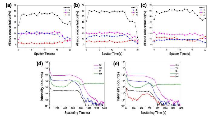
Fig. 5. AES depth profiles of O, Ti, Sr, and Al content as a function of depth in (a) STO layer, (b) Al40:STO layer, and (c) Al100:STO layer respectively. TOF-SIMS depth profiles near interfacial silicate region in (d) STO layer and (e) Al40:STO layer.
Overall, through XPS analysis, it is determined that the nonlinear relationships with the degree of Al incorporation (i.e., controlled by the RF power of Al source sputtering) are related to the changes in crystallization. When Al dopants were lightly introduced into the perovskite lattice of SrTiO3, the substitution and displacement of Ti lattice atoms increased the conduction band offset because of Al-doping-induced removal of the lattice distortion and increased charge trapping sites. This was also confirmed through UV-vis measurement in Fig. S4 (SI). The optical bandgap of SrTiO3 was considerably increased from 3.75 to 4.22 eV by Al doping with sp = 40 W. When the Al doping amount was higher (sp from 40 to 100 W), the Al:STO bandgap also increased but only slightly—from 4.22 to 4.30 eV. This was consistent with the excessive substitution and immigration of Ti and Sr lattice atoms, respectively; they caused disruptions in the crystallization of the SrTiO3 structure (i.e., short-range crystallization) and thus caused a change in the crystallization orientation (from (110) to (200)) and a high surface roughness of Al:STO in Fig. 2(b and c). Owing to the increase in the grain boundaries and unsaturated bonds of metal ions with oxygen on the sample surface, the insulator layers possessed more positive charges, which caused a risk of leakage current and compensated the bandgap widening. Due to the higher possibility of leakage current, it would be easier for the Al:STO samples with high Al doping amounts to lose their capacitance. From Eq. 1, the reason for the negative shifts of VFB is revealed.
$V_{FB}=\phi_{ms}-\frac{Q_{fixed}}{C_{i}}$ (1)
where Qfixed is the oxide trap charge at the bulk and interface of the insulator; Ci is the capacitance of the insulator layer; ϕms is the work function difference between the metal gate electrode and the semiconductor. As the difference between the ϕms ϕms values of SrTiO3 and Al:STO samples is insignificant, the lower capacitance values (Ci) of the Al:STO samples increased the voltage across the insulator (Vi = Qacc/Ci), resulting in more negative values of VFB. Fig. 5(a-e) shows AES and SIMS depth profiles, which were measured to trace elemental distribution in the bulk and interfacial oxides in MOS gate stack with increasing Al concentration. As Al content was increased, there is no marked change in Sr distribution, but it is observed that Ti decreases gradually toward Si interface and for Al40:STO layer, Al content dominates Ti content in vicinity of the bottom interfacial silicate (more clearly in SIMS data of Fig. 5(e)). It has been considered that Ti-silicate is highly defective because of chemical phase separation upon thermal crystallization (i.e., the mixed phase boundary defect of nanocrystalline transition metal oxide phase and amorphous SiOx phase). [40] However, the proper Al content at the interface replaces Ti and arises amorphous stabilization of Al-rich silicate with a much less defect density. Besides, SIMS results in Fig. 5(e) reveal the nature of interfacial SiOx layer (at about the sputtering time of 700-900 s) which consists of a mixture of multiple oxides with oxygen concentration insufficient to form SiO2. This oxygen-deficient SiOx layer has a negligible contribution to the dielectric properties, particularly leakage current in the gate stack. That is confirmed by J-V result in Fig. S6, where the Al-doping led to a large leakage reduction in both MIM and MOS structures while the leakage current density of the MIM structure without SiOx layer is not much different from that of MOS structure having the SiOx layer. Therefore, Al-doping played a decisive role in the control and optimization of STO dielectric property.
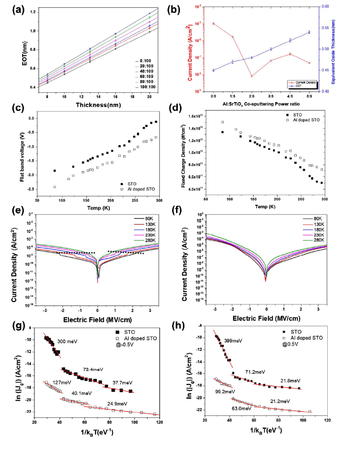
Fig. 6(a) shows the EOT values calculated corresponding to different thicknesses (di) of the insulator layers (8-20 nm). The dielectric constant (ki) of the SrTiO3 and Al:STO layers and the EOT values were calculated based on Eqs. 2 and 3. The results are summarized in Table 2.
$C=k_{i}\varepsilon_{0}\frac{A}{d_{i}}$ (2)
$EOT=d_{i}\frac{K_{SiO_{2}}}{k_{i}}$ (3)
Here, A is the dielectric area ( = 1 mm2) and kSiO2 is the dielectric constant of SiO2. The dielectric constant value of SrTiO3 is calculated to be 86.7, whereas that of Al:STO with sp ranging from 20 to 100 W is 83.6, 81.3, 78.2, 75, and 72.3, respectively. Fig. 6(b) shows a graph comparing the current density (at 1 MV/cm) and the EOT values of 8-nm-thick SrTiO3 and Al:STO samples. These values were extracted from Fig. 3. As shown here, despite the nonlinear shifts of the flat band voltage (VFB) in the negative direction with the Al doping amount, the maximum capacitance density of the Al:STO samples decreased (the EOT values of the Al:STO samples increased) in proportion to the increase in sp because the dopant content was approximately 10% or less in the SrTiO3 host. The leakage current density decreased for sp ≤ 40 W, increased for sp = 40-80 W, and then decreased for sp ≥ 80 W. This nonlinear behavior of the leakage current was explained through XPS analysis. Overall, among all 8-nm-thick samples, Al40:STO is the optimum sample, showing the lowest leakage current but a high capacitance, and thus, its dielectric constant (∼81.3) is maintained well. The obtained results may satisfy the requirements of future logic gate stack and DRAM capacitor applications.
Fig. 6. (a) EOT values of Al:STO layers (corresponding to different thicknesses) measured at a frequency of 1 MHz. (b) Comparison of the current density and EOT values of 8-nm-thick insulating layers. (c) Shift of flat band voltage through C-V measurement of the MOS devices (STO and Al:STO) with temperature variation from 80 to 300 K. (d) Variation of fixed charge density from the C-V measurement of the MOS devices (STO and Al:STO) with temperature variation from 80 to 300 K. Change in the leakage current tunneling model according to the electric field of (e) Al-doped STO film and (f) STO film at low temperature (80-280 K). Leakage current plots as a function of Arrhenius input with an increase in temperature (80-400 K) at (g) -0.5 V and (h) 0.5 V.
Table 2 Summary of the leakage current density, maximum capacitance density, EOT, and dielectric constant of SrTiO3 and Al:STO thin films.
| Sample (8 nm thick) | Leakage Current Density (A/cm2) (@1 MV/cm) | Capacitance Density (μF/cm2) | EOT (nm) | Dielectric constant |
|---|---|---|---|---|
| SrTiO3 | 1.02 × 10⁻⁵ | 7.67 | 0.45 | 86.7 |
| Al20:STO | 1.68 × 10⁻⁶ | 7.40 | 0.47 | 83.6 |
| Al40:STO | 2.53 × 10⁻⁹ | 7.20 | 0.48 | 81.3 |
| Al60:STO | 6.69 × 10⁻⁸ | 6.93 | 0.50 | 78.2 |
| Al80:STO | 1.67 × 10⁻⁷ | 6.64 | 0.52 | 75.0 |
| Al100:STO | 4.84 × 10⁻⁸ | 6.40 | 0.54 | 72.3 |
For physical analysis, C-V measurements of MOS devices were performed over the low-temperature range 80-300 K, which minimized thermal scattering (Fig. 6(c,d)). As a result, a large VFB shift was observed in the C-V graph with the increase in temperature. This can be deduced from the fact that the electrons activated by the increase in temperature interact with VO (oxygen vacancy), causing the VO-induced interface dipoles to change, resulting in the VFB shift. [41] It is also confirmed that the fixed charge density decreases as electrons are injected into VO as compensating positive fixed oxide charges. When the STO dielectric film was compared before and after Al doping, it was confirmed that the above effect was reduced in the case of doping with Al (230-300 K). Fig. 4(c) shows that the oxygen vacancy decreases and the Al-O bond increases after Al doping (Al40:STO); therefore, upon Al doping, the VO-induced effect in C-V analysis is reduced because the sample has a relatively low intrinsic VO density.
The low-temperature measurement was carried out to confirm only the tunneling effect, except for the thermal vibration effect of the current. I-V measurements of the MOS devices were obtained from 80 to 300 K (Fig. 6(e and f)). In the case of STO, the leakage current is developed as a Poole-Frenkel (P-F) model. P-F conduction is affected by trapping from bulk and activation of trapped carriers as expressed in Eq. 4. [41] However, after doping, the current follows a different tunneling model. At lower voltages, direct tunneling (as expressed in Eq. 5) and trap-assisted tunneling (as expressed in Eq. 6) currents flow. Thus, all carrier transport occurs across the defect in the dielectric layer. [42] However, as the voltage increases, the Fowler-Nordheim regime is reached. Therefore, the reduction of leakage current by doping can be effectively explained by the change of the tunneling model. Also, plots for each case are shown in Fig. S3 (SI).
$J_{PF}=E·exp[\frac{-q(\Phi_{t}-\sqrt{\frac{qE}{\varepsilon \pi}})}{kT}]$ (4)
$J_{TAT}=\frac{2C_{t}N_{t}q \Phi_{t}}{3E_{ox}}exp(\frac{8\pi\sqrt{2qm_{ox}}}{3h}\frac{\Phi^{3/2}_{t}}{E})$ (5)
$J_{FN}=AE^{2}exp(-\frac{B}{E})whereA=\frac{q^{3}m_{e}}{8\pi hm\phi_{B}}and\ B=4\sqrt{\frac{2m\phi^{3/2}_{B}}{3q \hslash}} $ (6)
In Fig. 6(g and h), the activation energies in the leakage current characteristics were calculated for the STO and Al40:STO MOS capacitors using Arrhenius plot (ln(J) / T-1) from 80 to 400 K. Because of the asymmetric structure of the MOS capacitor (i.e., carrier injection at Pt/STO interface under the negative bias and at STO/Si interface under the positive bias), the activation energy values were calculated at both ±0.5 V, considering different charge transport mechanisms as a function of temperature. It is observed from Fig. 6(g,h) that the activation energy for both STO and Al:STO in general increased with increasing temperature. However, the relative values of their activation energies are distinguishable. At 80-280 K (40-120 eV-1), the activation energies are slightly higher for STO than for Al:STO. At >280 K (40 eV-1), an outstanding difference in their activation energies is observed. Here, the activation energy of STO is about 3-4 times higher than that of Al40:STO at 0.5 V in Fig. 6(h). Based on the difference in activation energies and levels of Jg as a function of temperature, it is suggested that thermally activated trap states are different between STO and Al:STO. In the low-temperature region, P-F is relatively suppressed whereas trap-assisted tunneling is a dominant mechanism for the leakage current with a weak temperature sensitivity, but as temperature increases above 280 K, P-F becomes dominant, reflecting the strong dependence of oxygen-vacancy-associated shallow trap depth on the conduction band (CB) minimum. This implies that STO has the trap energy depth of 0.3-0.4 eV with high trap density but Al:STO has a much shallower trap energy depth of 0.1-0.15 eV with low trap density.
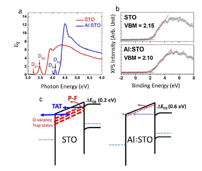
To correlate such electronically resolved trap states to spectroscopically resolved intrinsic defect states, spectroscopic ellipsometry (SE) analysis was performed to show the plot of imaginary dielectric function (ε2) in Fig. 7(a), which revealed spectral features with a better energy precision than the absorption coefficient plot. Three-phase optical modeling [43] was applied to extract the dielectric overlayer from the STO/Si and Al:STO/Si samples. Noticeable differences in ε2 spectra are seen at the absorption onset energies (3.7 eV for STO and 4.2 eV for Al:STO) and conduction band features at the photon energy above each absorption onset energy. Based on the Tauc plot, the direct bandgaps of STO and Al:STO were, respectively, considered 3.8 and 4.3 eV; this confirms the increase in bandgap by 0.5 eV with Al doping. Furthermore, ε2 spectra reveal (i) the defect energy depth at 0.4 (at defect onset, Ds1 level) and 0.2 eV (at defect center, Ds2 level) for STO and (ii) the defect energy depth at 0.15 (at defect onset, DA1 level) and 0.1 eV (at defect center, DA2 level) for Al:STO against the absorption onset energies of each dielectric (i.e., CB minimum energies). In addition, the defect absorption level of STO is higher than that of Al:STO in Fig. 7(a). Therefore, SE identified the intrinsic defect states and their energy levels are consistent with the electronically resolved trap state, indicating that Al doping controls the CB minimum of STO, increases the CB offset between Al:STO and Si, and reduces O-vacancy defect states. The physical origin of band electronic modification of STO with Al doping is considered, as the CB minimum level is raised by the higher-lying Al4s molecular orbital (MO) states than Ti3d, and subsequently, the band gap is increased (i.e., conduction band offset increases). In addition, Al4s states passivate unsaturated Ti3d states (due to O-vacancy defect states), which originally serve as shallow trap states in undoped STO. This idea of modified CB edge with Al doping is also reinforced by XPS valence band (VB) edge spectra (Fig. 7(b)), which show no significant difference between the VB maximum energy with and without Al doping as its orbitals mainly consist of Ti3d and O2p nonbonding MO states with less overlap of Al4s lower-lying bonding MO state. Finally, combining compensating data of ln(Jg) vs. 1/kBT and ε2 vs. photon energy, the schematic band-alignments of STO and Al:STO MOS capacitors under positive bias are constructed in Fig. 7(c). This band alignment shows a leakage current weakened by both P-F and trap-assisted tunneling mechanism for Al-STO owing to increased CB offset and fewer trap states.
Fig. 7. (a) Imaginary dielectric constant plot as a function of photon energy obtained from SE measurement and 3-phase optical modeling, (b) VB edge spectra obtained through XPS analysis for STO and Al:STO dielectric layers. (c) Schematic band alignment model constructed through electrical and spectroscopic analyses for STO and Al:STO MOS capacitors.
In summary, the dielectric thickness of SrTiO3-based-MOS capacitors was successfully reduced to 8 nm but they still maintained good performance values of leakage current (<10-8 A/cm2 at ±0.5 MV/cm), EOT (<5 Å), and dielectric constant (> 81). This was achieved by the introduction of Al dopant through a single-step co-sputtering process with the aid of PDA. The optimum sputtering power ratio of Al to SrTiO3 was determined to be 40:100 W. The co-sputtering method has the advantage of two aspects: it enables the uniform doping of Al to induce efficient reduction of leakage current. In addition, the concentration of Al can be easily controlled by changing the sputtering power. This approach is highly effective to control the leakage current level as it modifies the CB edge states with an increased bandgap and CB offset and reduces O-vacancy-associated shallow trap states, which cause P-F and trap-assisted tunneling as a function of temperature. Both electronic and spectroscopic analyses suggest that the bandgap and CB offset increase by > 0.6 eV and the defect density significantly decreases. Therefore, the possibility of applying our promising Al:STO material to manufacturing practical MOS capacitors well as MOS field-effect transistors is confirmed. Further studies on improving uniformity of doping can be attractive because the uniform insertion of dopants through ALD is more likely to be compatible for a high-aspect-ratio MIM capacitor in DRAM as well. From this viewpoint, there are still possibilities to reduce the level of leakage current and ensure good capacitance values of ultrathin MOS capacitors based on SrTiO3 with dopants through different deposition techniques.
This work was supported by National Research Foundation of Korea [NRF-2019R1A2C2003804 and 2018H1D3A1A02074733] of the Ministry of Science and ICT, Republic of Korea and the technology development program (G21S272158901) funded by the Ministry of SMEs and Startups, Republic of Korea. This work was also supported by Ajou University.
Supplementary material related to this article can be found, inthe online version, at https://doi.org/10.1016/j.jmst.2019.12.006.

 WeChat
/
| 〈 |
|
〉 |