Search for articles:
Edson Cezar Grzebielucka , João Frederico Haas Leandro Monteiro
Corresponding authors:
Received: 2019-07-2
Revised: 2019-08-7
Accepted: 2019-08-20
Online: 2020-03-15
Copyright: 2020 Editorial board of Journal of Materials Science & Technology Copyright reserved, Editorial board of Journal of Materials Science & Technology
More
Abstract
The effect of chromium addition on the structure and electrical properties of CaCu3Ti4O12 is studied. Compositions based on the formula CaCu3Ti4-xCrxO12-δ (x = 0, 0.025, 0.050 and 0.075 mol%) are prepared by solid-state reaction. Pellets sintered at 1070 °C for 12 h are characterised by X-ray diffraction, scanning electron microscopy/energy dispersive spectroscopy and impedance spectroscopy. Current density-electric field, dielectric loss and permittivity measurements are also carried out. Rietveld refinement showed the substitution of Cr(III) on the Ti(IV) site, with the maximum substitution for x = 0.025 mol%. The generation of electrical defects in the grain boundary region by chromium doping is responsible for increasing the electric breakdown field strength and nonlinearity coefficient at room temperature from 1723 V/cm and 5.29 for x = 0 mol% to 3431 V/cm and 8.16 for x = 0.025 mol%. This composition shows the greatest improvement in ceramic varistor parameters.
Keywords:
The increasing use of electronic products has driven the development of devices that electrically protect these appliances from overvoltages caused by fluctuations in the electrical network. Varistors are devices that are used for this purpose and can generate protection against both small and large voltage variations. The parameter of the electric breakdown field strength (Eb) and nonlinearity coefficient (α) determines the material application range as a varistor. Thus, the higher these parameters, the greater the capacity to protect in case of electrical overload [1]. Perovskites formed by the CaCu3Ti4-xCrxO12-δ series have received attention as candidates to be applied as varistors due to the formation of electrical defects as a result of Ti4+ replacement by an M3+ element. This doping tends to highlight even more its high dielectric permittivity (ε'), in addition to modifying the two parameters cited previously [[2], [3], [4]].
As discussed, varistors are electronic ceramic-based devices whose function is to protect electrical systems from overvoltage without being destroyed, unlike fuses that rupture when exposed to an overcurrent. The range of their application varies from a few volts to kilovolts and they can be used in fields of continuous or alternating current from microamperes to kiloamperes. They are also called voltage-dependent resistors due to their nonlinear current-voltage (I-V) characteristic. They show high resistivity in the pre-breakdown region, i.e., the ohmic region, and a large non-linearity coefficient. TiO2, WO3, ZnO, SnO2 and SrTiO3 are some examples of materials that show the varistor effect [5].
Dependence on the nonlinearity coefficient for non-ohmic ceramics is defined by Eq. (1), where I is the current, V is the electric potential and K is a constant related to the microstructure of the material. If α assumes a value equal to 1, the current becomes proportional to the applied voltage. Thus, the greater the value of α, the greater the non-ohmic response. An ideal varistor is one in which the current varies infinitely for small changes in the applied field [5,6].
I=KVα (1)
Electronic species diffusion (dopants, interstitial atoms, vacancies, association of electronic defects and so on) to the region between grain boundaries is responsible for a potential barrier formation. The grain boundary core is a region with a thickness of some lattice parameters, formed by atoms from different crystalline directions with incomplete chemical bonds, which generate an excess of free energy. This in turn leads to depletion or accumulation of ionic and/or electron species at the grain boundary core. The concentration of these species in the grain boundary core increases, leading to the formation of a space charge layer. Oxygen vacancy depletion in the space charge layers occurs because of the positive charge of the grain boundary core. The space charge loads arise from the segregation of trivalent dopants near the grain boundary, generating a space charge potential that blocks vacancy movements [7].
CaCu3Ti4O12 (CCTO) is a ceramic with the perovskite-type structure and has attracted significant interest due to its high dielectric permittivity (up to 105), which is almost frequency-independent up to kHz values and is weakly dependent on the temperature in the range between 100-400 K [8,9]. However, the origin of this unusual dielectric behaviour is still controversial. The widely accepted mechanism is the internal barrier layer capacitor, in which the material is considered as being composed of semiconductor CCTO grains and a very thin copper-rich secondary phase observed between the grains, forming insulating barriers [[10], [11], [12], [13], [14]]. The significant difference between the electrical properties in grains and at grain boundaries leads to electrostatic barriers known as Schottky potential barriers. The Schottky potential barriers inhibit the electronic transport and establish a large boundary polarisation, resulting in a giant dielectric permittivity and characteristic non-ohmic behaviour in the electric conduction [12,15].
The Schottky potential barrier can evaluate the effect of a dopant by the β constant, which is related to the width of the space charge layer (w) by employing Eq. (2), where n is the number of grains per unit length [16].
$β∝1/(n∙w)^{\frac{1}{2}}$ (2)
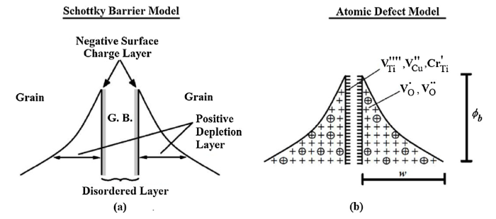
The β constant can be obtained directly by means of the slope of the line obtained by the graph of ln J vs $\sqrt{E}$ for each temperature and composition studied, where J and E are the current density and electrical field, respectively. Taking the ln J values for each measured temperature, when $\sqrt{E}$=0 and plotting it as a function of the inverse of the same temperature (1/T), the slope of the line, the Schottky barrier height (φb) can be obtained by the slope. This Schottky barrier is needed to promote the charge carrier jump from an equilibrium position to another adjacent free position. Fig. 1(a) exemplifies the negative charge distribution pattern on the grain boundary surface while positive charges are concentrated inside in the bulk regions, adjacent to the grain boundary, according to the Schottky barrier model.
Fig. 1. (a) Schottky barrier model for atomic defect model on the grain boundary (G.B.) showing different places with negative and positive charge concentration and (b) the similar atomic defect model proposed for CCTO by Cr2O3 addition on the Schottky barrier height (φb) and the space charge layer, adapted from Gupta and Carlson [
Regarding CCTO, many studies have already investigated the improvement of electrical properties using dopants [[17], [18], [19], [20]], the origin of the colossal permittivity [8,21,22] from different points of view and the results were published including single crystals [9,21,23], thin films [[24], [25], [26]] and polycrystalline samples [9,11,27,28].
The literature has shown some results obtained using different dopants. Wang et al. [17] using 5 mol% of Co (CaCu2.95Co0.05Ti4O12) obtained α = 5.22 and Eb = 300.46 V/cm [17]. When using 20 mol% of Ni (CaCu2.8Ni0.2Ti4O12), they found α = 5.47, Eb = 101.7 V/cm [18]. Liu et al. [19] have studied various dopants and obtained values of α and Eb from NiO (3.66, 316.9 V/cm), SnO2 (3.77, 485.7 V/cm), SiO2 (2.75, 296.6 V/cm), Al2O3 (3.74, 1390.7 V/cm), respectively. Doping with Sr and Ni was studied by Rhouma et al. [20], those authors found α = 5.88, Eb = 0.60 kV/cm and leakage current (IL) of 200 μA/cm2 (Ca0.9Sr0.1Cu3Ti4O12) and α = 8.33, Eb = 0.58 kV/cm and IL =130 μA/cm2 (CaCu2.9Ni0.1Ti4O12).
However, although there is a patent showing the application of CCTO as a varistor candidate due to its non-ohmic characteristics [29], it does not cover the possibility of substitution at the B site, which is the situation proposed in this work. Dielectric behaviour can be manipulated through several modifications in the chemical composition, as well as the preparation of the material.
The substitution of Cu(II) by divalent cations was observed to modify the dielectric properties of CCTO. Using Zn(II), a reduction in the tanδ value was obtained between 0.016 and 0.017 with a dielectric permittivity between 6500 and 7700 at 1 kHz [30]. Using Mg(II) instead of Cu(II) and Sm(III) instead of Ca(II) the dielectric permittivity increased to 1.25 × 10⁴ and the tanδ value was 0.039 at 1 kHz [31]. Choi, Hong and Kim [32] studied the effect of Al-doped CCTO ceramics. They showed that reduced dielectric loss (tanδ below 0.06 over the frequency range 102-104 Hz) while maintaining a high dielectric permittivity lies on the enhancement of grain boundary resistivity. Luo, He, Hu and Lin [33] studied Bi-doped CCTO prepared by solid-state sintering, and they found a new phase (Bi4Ti3O12) and showed that the grain size can be controlled by bismuth content, as well as a decrease in the dielectric loss but deteriorating the dielectric temperature stability simultaneously. Bi-doped CCTO was also studied by Xu et al. [34], but they prepared solid solutions where Bi substituted Ca. Recently, Ren et al. [35] studied CCTO ceramics co-doped with Bi(III) and Al(III) showing an improvement in the varistor properties with respect to CCTO. In this work, the substitution of Ti(IV) by Cr(III) in the CCTO structure was proposed to modify the Schottky barrier and to enhance varistor characteristics.
Based on the previous model, Figs. 1(a) and 1(b) show a distribution scheme of the possible defects with a negative effective charge ($V_{Ti}^{''''}$, $V_{Cu}^{''}$ and $Cr_{Ti}^{'}$) at the grain boundary interfaces, in the case of chromium doping, and defects with positive effective charge ($V_O^∙$ and $V_O^{∙∙}$) in the region adjacent to the grain boundary, adapted from the Gupta model [36]. Thus, the ideal conditions to obtain a material with varistor characteristics with a high value of nonlinearity coefficient is that in the grain boundary region in which the potential barrier is high and narrow [6].
In the present work, different compositions of Cr(III) doped CaCu3Ti4-xCrxO12-δ were prepared by solid-state reaction, in order to analyze the influence of this element on the electric and dielectric properties of this material to be used as a varistor.
The solid-state reaction method was employed to prepare polycrystalline samples of CaCu3Ti4-xCrxO12-δ (x = 0, 0.025, 0.050 and 0.075 mol%). Appropriate amounts of analytical grade CaO (NUCLEAR - 95.0 %), anatase TiO2 (VETEC, 99.5 %), CuO (SYNTH, 99.0 %) and Cr2O3 (Dinâmica, 99 %) powders were mixed for 2 h, by means of ball milling with zirconia balls using isopropyl alcohol as a liquid medium. The milled powders were dried at 100 °C. The powders were calcined at 1000 °C for 12 h twice with intermediate grindings. Powders were dried again and uniaxially pressed into discs with a 13 mm diameter and a ∼1 mm thickness at 74 MPa. The pellets were sintered in air at 1070 °C for 12 h and afterwards were slowly cooled inside the furnace up to room temperature. Table 1 shows the adopted composition and the respective samples identification used in this study.
Table 1 Prepared compositions for xmol% addition of chromium in the CaCu3Ti4- xCrxO12-δ and the respective sample identification adopted.
| x mol% in CaCu3Ti4-xCrxO12-δ | Composition | Sample ID |
|---|---|---|
| 0.000 | CaCu3Ti4-xCrxO12-δ | CCTO |
| 0.025 | CaCu3Ti3.975Cr0.025O12-δ | Cr_025 |
| 0.050 | CaCu3Ti3.950Cr0.050O12-δ | Cr_050 |
| 0.075 | CaCu3Ti3.925Cr0.075O12-δ | Cr_075 |
The phase composition and crystal structure were characterised using X-ray diffraction (XRD) with a Shimadzu diffractometer XRD-6000 with CuKα1 radiation, λ =1.5406 Å. The unit cell parameters were refined using the Rietveld method assisted by FullProf software [37]. The diffraction patterns were collected over the range 5° to 100° in the 2θ range with 0.02° step and a 5 s counting time for the ground sintered samples. The microstructure was observed with scanning electron microscopy (SEM) and with energy dispersive spectroscopy (EDS) in a model Tescan-Mira3 LM.
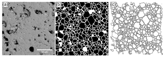
The average grain size was calculated through the statistical analysis of five micrographs obtained by SEM of each sample after being polished and thermally attacked by ImageJ software, according to ASTM E 1382-97 [38]. The Feret parameter was used as the determination criterion, which considers an average between determined sizes in the X and Y axes of a grain and not only the area of the grain. The digital processing of the micrographs followed was similar to that proposed by Marcomini [39], according to the example of Fig. 2.
Fig. 2. Example image processed by ImageJ software for SEM image of polished and thermally attacked CCTO (a), converted image for binary (b), and (c) whole grains counted without considering pores.
For the electrical property measurements, the surfaces of the sintered CaCu3Ti4-xCrxO12-δ ceramics were polished. Then, electrodes were fabricated on opposite pellet faces from Ag paste, which was dried and decomposed by gradually heating at 700 °C for 30 min. Samples with electrodes attached were measured using a Solartron 1260A analyser over the frequency range 10-1 to 107 Hz and at temperatures ranging from 100 to 200 °C. Impedance data were corrected for overall pellet geometry and measurements were carried out in air atmosphere with an AC measuring voltage of 1 V.
Current density-electric field (J-E) characteristics were measured from 20 to 150 °C using a high voltage measurement unit (Keithley 2410) with sweep delay of 100 ms and a rising rate of voltage of 18 V/s. The electric field breakdown value (Eb) was obtained directly from the J-E curves for values of J = 1 mA/cm2, value established in literature [40,41]. Leakage current values (IL) were obtained at 0.7Eb and the nonlinearity coefficient (α) was obtained by means of the angular coefficient from curve ln J vs ln E, according to Eq. (3), where E1 and E2 are the electric fields corresponding to J1 = 1 mA/cm2 and J2 = 10 mA/cm2, respectively [40,41].
α=$\frac{(ln\ J_2-lnJ_1)}{(lnE_2-ln\ E_1)}$ (3)
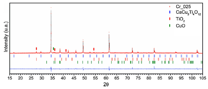
XRD analysis of pure CCTO confirmed CaCu3Ti4O12 phase formation (PDF 75-2188) as the majority phase at a sintering temperature of 1070 °C for 12 h. However, the diffraction pattern also revealed the presence of TiO2 (PDF 65-1118) and CuO (PDF 89-5899) phases. Peaks of CuO could also be found in the samples due to the segregation of CuO at high temperatures (>1000 °C), forming a liquid phase during the sintering treatment, in agreement with previous reports [2,11,35,42]. The segregation of the CuO phase could also justify the presence of TiO2, as we will discuss later. The Rietveld refinement confirmed the presence of CaCu3Ti4O12 (ICSD 32,002) in the cubic symmetry (Im$\bar{3}$, n° 204), as the major phase, with 90.6% in mass, and the other phases, TiO2 (ICSD 88,626) in tetragonal symmetry (P42/mnm, n° 136), and CuO (ICSD 87,122) in the monoclinic symmetry (C2/c, n° 15) with 4.2% and 5.2% by mass, respectively. Fig. 3 shows the final refinement profile obtained for the CCTO sample diffraction pattern, where the reflections for the remaining TiO2 phase corresponded to the planes (110), (101) and (211), respectively, and for CuO (1$\bar{1}$1).
Fig. 3. Rietveld refinement XRD pattern for pure CCTO, sintered at 1070 °C for 12 h, showing Bragg positions for CaCu3Ti4O12 (blue bar), TiO2 (red bar) and CuO (green bar) phases.
Using the Rietveld refinement of CCTO as a reference, the refinements of the other diffraction patterns obtained with the addition of different amounts of chromium in the perovskite CaCu3Ti4-xCrxO12-δ were carried out for the same sintering condition as that used with CCTO. The final refinement profile obtained for the sample Cr_025 is shown in Fig. 4, which is representative of all other refined compositions. In the same way as the CCTO sample, the same residual TiO2 and CuO phases were also observed for all compositions, but the least segregation occurred for the Cr_025 sample. The main parameters measured for the CaCu3Ti4-xCrxO12-δ series are grouped in Table 2. Refinement quality is evaluated by a series of indexes, with the index Rp being the profile factor, Rwp the weighted-profile factor, Rexp the statistically expected factor and RB the quality of the proposed structure for the diffraction profile obtained for the Bragg reflection. A relation between the quality of fit, χ2, and the reliability index, S, is given by Eq. (4), which must present values between 1 ≤ S ≤ 2, and the closer to S = 1 they are, the more reliable the results obtained through refinement are [43]. Thus, all the refinements performed presented low and acceptable reliability index values, which denote the quality of the refinements performed in all the compositions studied.
S=$\sqrt{χ^2}=\frac{R_{wp}}{R_{exp}}$ (4)
Fig. 4. Rietveld refinement XRD pattern for Cr_025 sample, sintered at 1070 °C for 12 h, showing Bragg’s positions for CaCu3Ti4O12 (blue bar), TiO2 (red bar) and CuO (green bar), phases.
Table 2 Comparison of measured structural parameters of CCTO and the compositions prepared with different amounts of chromium. CCTO shows space group Im$\bar{3}$; the Wyckoff positions are Ca(0,0,0), Cu(1/2,0,0), Ti-Cr(1/4,1/4,1/4) and O(x,y,0). Numbers put in brackets correspond to standard deviation referenced to the last number for all parameters measured.
| Parameters | CaCu3Ti4-xCrxO12-δ Phase | |||
|---|---|---|---|---|
| CCTO | Cr_025 | Cr_050 | Cr_075 | |
| wt% | 90.6 | 91.5 | 88.2 | 90.2 |
| a (Å) | 7.38921(4) | 7.39255(6) | 7.39122(4) | 7.39023(4) |
| V (ų) | 403.454(4) | 404.001(6) | 403.783(4) | 403.621(4) |
| d (g/cm³) | 4.928 | 4.686 | 4.887 | 4.837 |
| x | 0.2997(7) | 0.3034(8) | 0.2978(7) | 0.3047(7) |
| y | 0.1814(7) | 0.1809(8) | 0.1820(7) | 0.1790(7) |
| TiO2 wt% | 4.2 | 3.4 | 4.9 | 4.2 |
| CuO wt% | 5.2 | 5.1 | 6.9 | 5.6 |
| Rp | 6.24 | 7.12 | 6.13 | 5.76 |
| Rwp | 7.95 | 9.61 | 7.82 | 7.69 |
| RB | 6.65 | 6.63 | 6.35 | 6.07 |
| Rexp | 6.12 | 6.47 | 6.05 | 5.34 |
| χ2 | 1.68 | 2.21 | 1.67 | 2.08 |
| S | 1.29 | 1.22 | 1.29 | 1.44 |
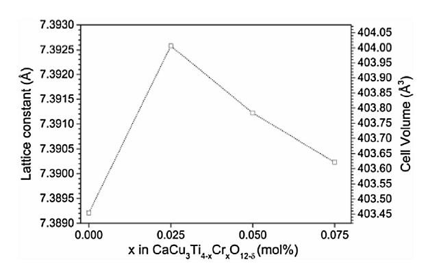
The lattice parameter obtained using XRD is very reliable since the scanning range of the samples (5°-110°) ensures mathematically a calculation of considerable precision. The lattice parameter value calculated for the CCTO was 7.389 Å, a value lower than that found in the literature (7.391 Å) [[44], [45], [46]]. Based on the ionic radius of Cr3+, 0.615 Å, and Ti4+, 0.605 Å with a coordination number of six [47], with the addition of chromium, a continuous increase in the lattice parameter with the amount of dopant is expected. Eq. (5) describes the defect reaction to the formation of an oxygen vacancy for every two chromium atoms in the titanium atomic position. However, this behaviour was only observed for the Cr_025 sample, Fig. 5, which compares the variation of the lattice parameter size and unit cell volume as a function of the amount of added chromium. The lattice parameter size behaviour is noticeably the inverse of that expected for chromium doping higher concentrations [48].
$Cr_2O_3\ \mathop{}_{→}^{TiO_2}\ 2Cr_{Ti}^′+VÖ+3O_O^x$ (5)
Fig. 5. Lattice constant and cell volume for pure CCTO and with addition of x mol% of chromium.
This behaviour could be explained using different arguments. One of them could be related with the maximum substitution that the perovskite CCTO tolerates to form a solid solution, confirmed by the increase in the lattice parameter to 7.392 Å. For values higher than that mentioned, an increase in the lattice parameter in relation to the CCTO occurs, but lower than that obtained with 0.025 mol% of Cr2O3.
Another possibility to explain this behaviour involves the reported reduction in Cu(II) to Cu(I) [42,49] as a function of heating oxides in air, which can further a slight substitution of Ti(IV) on the Cu site to maintain charge balance for the compound. The reduction of CuO to Cu2O promotes deviation in the stoichiometry that is too small to be detected by XRD data refining. During cooling, CuO is more stable than Cu2O resulting in the formation of Cu2-xO, CuO or Cu1-xO at the grain boundary. Electronic defects like $V_{Cu}^{'}$, $Cu_{Cu}^{'}$ or $V_{Cu}^{''}$ are formed at grain boundaries and can act as acceptors, forming double Schottky barriers with the n-type semiconductor grains. This implies the possible formation of vacancies of $V_{Ti}^{''''}$, $V_{Cu}^{''}$ and VO∙∙ in the CaCu3Ti4O12 structure, making it non-stoichiometric and distorted in structure. This fact directly affects the lattice parameter and consequently the cell volume of the CCTO, as observed in Fig. 5. Calculations using the density functional theory showed that when a copper vacancy is formed, a contraction of up to 7% occurs in the bonding distance between the oxygen atoms in the CuO4 planar unit of the CCTO network [45], justifying the lattice parameter reduction. The remaining TiO2 phase can probably be justified by decomposition of CaCu3Ti4O12 in CuO and Cu2O as predicted in the pseudo-ternary system CaO-CuO/Cu2O-TiO2 [50]. TiO2 and CuO phases are also described in other works with the CaCu3Ti4O12 system with other dopants, which used both solid-state reaction processing [13,51] and chemical synthesis [12,52].
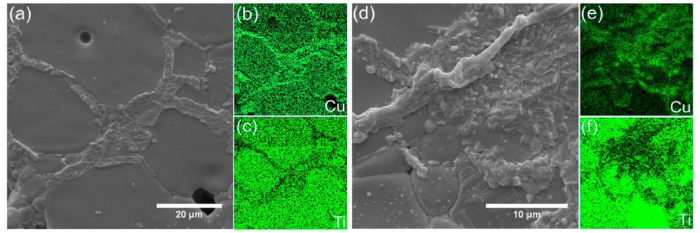
The SEM images are shown in Figs. 6(a) and (d) for the Cr_025 sample polished and thermally treated, confirming the presence of secondary phases quantified with CuO being found preferentially segregated at grain boundaries, as previously mentioned [[10], [11], [12], [13], [14]]. While a TiO2 phase was not found at the grain boundary, Fig. 6(c), being found in the form of deposits concentrated at some points on the Cr_025 sample polished surface, as evidenced by chemical mapping in Fig. 6(f), which identifies the strong element concentration of titanium in the prominent region. Cr_025 grains presented a homogeneous distribution of their constituent elements. All samples showed similar morphology, where the CuO and TiO2 phases segregated in the same regions as in the Cr_025, and the behaviour shown in Fig. 6 was representative of all other compositions.
Fig. 6. SEM images of two regions (a and d) of the Cr_025 sample polished and thermally treated, showing chemical mapping to CuO phase segregation on grain boundary (b) and (e) and showing absence of TiO2 phase segregation on grain boundary (c) and concentration of TiO2 at some grains with a surface texture (f). The elements O, Cr and Ca are homogeneously distributed.
Since only Cr_025 showed an increase in the lattice parameter with chromium addition, the electrical properties of this sample were compared to the CCTO and Cr_050 samples and the Cr_075 sample was discarded from the other characterisations.
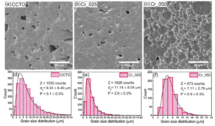
Fig. 7 shows the characteristic MEV images for the CCTO, Cr_025 and Cr_050 samples, where the average grain sizes (dg), grain size distribution and apparent porosity (P) are compared. For each sample, five images at the same magnification were used for grain size measurements, as shown in Fig. 2. The Cr_050 sample presented a higher quantity of CuO grains exuded after thermal treatment to reveal the grain contours, according to the Rietveld data refinement shown in Table 2. For that, CuO grains were not considered on the grain size measure, which explains the minor number of counts (Z) for the Cr_050 sample on contrast with the others. It was observed that the apparent porosity (P) values decrease with increasing Cr, with values of 9.1 ± 0.3 %, 2.6 ± 0.3 % and 0.9 ± 0.3 % for CCTO, Cr_025 and Cr_050, respectively. The average grain sizes (dg) obtained for samples were 8.34 ± 6.40 μm, 11.14 ± 8.04 μm and 7.11 ± 2.76 μm for CCTO, Cr_025 and Cr_050, respectively. The grain size distribution was asymmetric for the samples, so a logarithmic normal distribution was adopted. The range of sizes ranged up to 32 μm for CCTO, with a larger frequency for sizes between 2 and 10 μm, and up to 22 μm for Cr_050, with a larger frequency for sizes between 4 and 10 μm. The Cr_025 sample showed abnormal grain growth sizes up to 80 μm, with larger frequency for sizes below 15 μm.
Fig. 7. SEM image features used to measure the average grain size (dg), logarithmic normal grain size distribution and apparent porosity (P) for CCTO (a) and (d), Cr_025 (b) and (e), and Cr_050 (c) and (f).
The small amount of Cr added was responsible for improving the apparent densification of samples, with values of 4.36 ± 0.03 g/cm3, 4.63 ± 0.01 g/cm3 and 4.75 ± 0.01 g/cm3, which correspond to densifications of 88.5 %, 98.8 % and 97.2 % (calculated from the density obtained by XRD) for CCTO, Cr_025 and Cr_050, respectively. A decrease in the dg with increasing Cr(III) ions amount was expected [53], but only in the Cr_050 sample does this occur. A decrease in dg implies in an increase of potential barriers by increasing the number of grain boundaries [54].
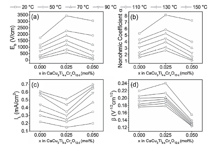
Nonlinear behaviour analysis between the electric current density (J) and applied electric field (E) showed that the addition of chromium provided a shift in the J-E curves to higher electric field values. An increase in the breakdown electric field (Eb) was observed for both samples with chromium when compared to the value of Eb of the CCTO at the same temperature, as shown in Figs. 8(a) to (c). A natural decrease in the breakdown electric field for all samples was observed at higher temperatures. A high Eb value was always obtained for the Cr_025 sample, Fig. 9(a). The breakdown electric field provided values that indicate the protection degree that a varistor will offer when an overvoltage occurs in the system and the type of application they are suitable for. They can be applied to small electrical circuit boards or lightning arresters [55].
Fig. 8. Current density (J) versus electrical field (E) for CCTO and for the compositions with different amounts of chromium at (a) 20, (b) 90 and (c) 150 °C.
Fig. 9. Comparison of measured electric breakdown field strength, Eb, (a), nonlinear coefficient, α, obtained between 1 and 10 mA/cm2 (b), measured leakage current, IL, calculated at 70% of the breakdown electrical field (c), and β constant that is proportional to the inverse of the square root of w (d) at the temperature range 20-150 °C for CCTO and for the two compositions studied.
Comparing the values of electric field breakdown at 20 °C, the addition of chromium increased the Eb values, as shown in Fig. 9(a). The addition of 0.025 mol% chromium caused a greater increase in the electric field breakdown with a value of 3431 V/cm at 20 °C and 568 V/cm at 150 °C, when compared with 1726 V/cm and 128 V/cm of CCTO at the same temperatures. Electric field breakdown values for the CCTO found in the literature at room temperature are 5.8 V/cm [14], 147.07 V/cm [31], 233 V/cm [30], 300 and 1300 V/cm [56]. These values are lower than the CCTO, 1726 V/cm; Cr_025, 3431 V/cm; Cr_050, 3051 V/cm; showing great divergence of this parameter. The values of Eb obtained indicate that any samples with the addition of chromium can be used as varistors at room temperature, considering only the Eb criterion for material selection.
No trend was observed between the dopant amount and the electric field breakdown at the same temperature or with the increase in temperature (Fig. 9(a)), only that chromium addition led to an increase of Eb for any amount. This can be justified by the increase in the lattice parameter of CCTO when Cr is added, but there was only a significant increase in the concentration of 0.025 mol%. Thus, if Cr(III) occupies the network position of Ti(IV), an increase in the concentration of positive charges in the region close to the grain boundary is expected, increasing the width of the potential barrier and increasing the Eb value.
A reduction in Eb values with increasing temperature is expected and justified by the reduction in the Schottky potential barrier in the grain boundaries and by the emission of thermionic current through the Schottky potential barrier [55]. Cr(III) doping at the B site of Ti(IV) promotes the creation of electron acceptor levels above the TiO2 valence band. This p-type doping increases the resistivity or decreases the conductivity of TiO2, as can be observed by adding 0.025 mol% chromium to the pure CCTO, where an electric field rupture occurs. The electric conduction at low applied electrical field in these ceramics is governed by the thermionic effect of the Schottky type. Thus, the increase in temperature in the region of low electric field leads to an increase in electrical conduction. At high temperatures, the electric conduction mechanism by tunnelling of electrons by the potential barrier happens to dominate. Thus, when raising the temperature, for different compositions, the conductivity tends to be the same.
Nonlinearity coefficient values (α) as a function of temperature are compared in Fig. 9(b). They indicate that the chromium had a positive effect by providing an increase in this parameter at room temperature from 5.29 (CCTO) to 8.16 (Cr_025), but not for Cr_050 (7.33), due to non-substitution of Ti (IV) by Cr (III), as shown in the reduction of the lattice constant in Fig. 5.
The α value of 5.29 obtained for CCTO is within the same magnitude found in the literature for CaCu3Ti4O12 of 2.96 [31], 3.32 [30], 4.37 [35], values lower than the one obtained in this work for Cr_025. Some discrepant values for α using Cr(III) as dopant were reported from synthesis by polymer pyrolysis [53,57]. In the study of Prompa, Swatsitang and Putjuso [53] was obtained values of α and Eb of 234.24 and 10,197.75 V/cm, respectively, for the composition CaCu2.95Cr0.05Ti4.1O12, Cr(III) being a substituent for Cu and not for Ti, as proposed in this work. In addition, the authors did not mention the densification and apparent porosity values. The microstructure reported by the authors shows a considerable apparent porosity. It may be electrically acting as a second resistive phase in the grain boundary region, thus raising the value of α.
The values of α and Eb obtained show that the developed compositions present better or similar performance to those presented in the literature [[17], [18], [19], [20]], even when compared with other dopants and in larger quantities.
Similarly, in the study of Swatsitang and Putjuso [57] values of α and Eb of 114.4 and 8455 V/cm, respectively, were obtained for the composition CaCu2.92Cr0.08Ti4O12, with densification of 99.62% of the theoretical density obtained by XRD, with an average grain size of ∼60.3 ± 2.0 μm, not observing the secondary phase formation of CuO. For both studies [53,57] the substitution of Cu by Cr occurs, the plot of current of density as a function of the electric field (J-E) showed few points after the zone of rupture, which can statistically lead to possible errors in determining the value of the coefficient of nonlinearity. Neither of these studies [53,57] addressed the rising voltage rate in obtaining data during I-V measurement.
Lu et al. [58] showed in their work that CCTO presents an extremely strong nonlinear behaviour due to the thermionic emission current feedback amplification effect. Thus, the nonlinear coefficient of CCTO increases as the voltage rise rate decreases. In this work, a sweeping delay of 100 ms and a rising rate of voltage of 18 V/s were assumed. Therefore, the α values obtained in this work are within the range [58] in which the thermionic emission current feedback amplification effect does not interfere in the measurement of the nonlinear coefficient. Thereby, the improvement of the nonlinear coefficient observed for Cr_025 is only attributed to the Cr addition.
Thermal avalanche is a phenomenon in which a reduction in the nonlinearity coefficient occurs as the temperature increases [59]. The increase in temperature favours the mobility of the species located in the bulk that recombined with the species located in the grain boundary, facilitating the reduction in potential barrier height, allowing all current to cross the thickness of the sample, leading to material degradation [59]. This effect can be observed in Fig. 9(c), where the leakage current values obtained at 0.7Eb are compared, showing an increase in the IL values with the temperature for all compositions studied. Cr_025 presented lower leakage (0.15 mA/cm2) current values than CCTO (0.22 mA/cm2) at room temperature.
Variation of the β constant for the compositions studied as a function of temperature is shown in Fig. 9(d). At room temperature, the β constant increases for the Cr_025 sample when compared with CCTO and Cr_050, indicating the width of the space charge layer. This may indicate that a minor amount of positive species are concentrated around the grain boundary core. All samples show a decrease in the β constant with increasing temperature. The Schottky barrier height, φb, also changed with chromium addition, with increases from 0.62 eV for CCTO to 0.70 eV (Cr_025) and 0.73 eV (Cr_050). The two parameters β and φb provided indications that the creation of oxygen vacancies by the doping of the CCTO with 0.025 mol% of chromium definitely alters the distribution of electrical defects in the grain boundary region. This confirms the increase in the values of electric breakdown field strength with chromium doping. In addition, CuO was observed as the second precipitated phase in the grain boundary region (type II junction), which prevented the contact of CCTO grain boundaries (type I junction), where type I junctions favour the non-ohmic behaviour, unlike type II junctions [5].
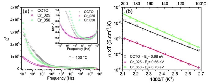
The frequency dependence of dielectric permittivity at 100 °C obtained from the impedance data for the three studied samples is shown in Fig. 10(a). Almost linear behaviour of ε' between 107 and 102 Hz for sample x = 0.025 mol% was observed. The dielectric permittivity values among 1 kHz and 1 MHz are listed in Table 3. The ε' obtained at the 1 kHz frequency for the CCTO samples containing chromium were very close to each other, but lower than for CCTO. The dielectric permittivity values obtained are in agreement with the giant values of dielectrics observed in the literature for CCTO [8,21,22]. The low-frequency region is attributed to the contribution of charge accumulation at the interface. At high frequencies, due to high periodic reversal of the field at the interface, the contribution of charge carriers to the dielectric permittivity decreases with increasing frequency. In contrast, the loss tangent or dielectric loss, inset in Fig. 10(a), provides information on how much the polarisation is delayed in relation to the applied electric field, so the lower the value is, the better the dielectric is. In view of this, chromium addition was efficient in reducing tanδ value at 1 kHz from 0.35 for CCTO to 0.20 for Cr_025 and 0.50 for Cr_050. The tanδ values obtained were higher than those for CaCu3Ti4O12 (0.108 [30] and 0.194 [31]) and were also much higher than those with doping of Zn(II) (0.017) [30], Sm(III) and Mg(II) (0.039) [31] and Zr(IV) (0.028) [2]. However, evaluating the tanδ value alone is not the most appropriate method without considering the values of the coefficient of non-linearity and electric breakdown field strength at the same time, (5,62; 1832 V/cm) [30] and (5,31; 1656 V/cm) [31], respectively, which were all lower than those obtained in this work. The tanδ value increase is justified by the increased conductivity observed for this sample, as observed by the higher IL value and lower value of the β constant. A small variation was observed in tanδ in the frequency range between 1 and 100 kHz for samples with chromium. Dielectric permittivity values and dielectric loss constants within a frequency range are of great importance for the manufacture of electro-electronic devices. Materials with high dielectric permittivity allow the use of dielectrics with much smaller dimensions.
Fig. 10. Frequency dependence of ε’ and inset shows tan δ, both at 100 °C (a) and electrical conductivity (b) for the compositions studied.
Table 3 Comparison of dielectric permittivity (ε') and tan δ at 100 °C as a function of frequency for CCTO and for the two compositions studied.
| Sample | 1 kHz | 10 kHz | 100 kHz | 1 MHz | ||||
|---|---|---|---|---|---|---|---|---|
| ε' | tan δ | ε' | tan δ | ε' | tan δ | ε' | tan δ | |
| CCTO | 14944 | 0.35 | 12467 | 0.14 | 10562 | 0.15 | 7898 | 0.423 |
| Cr_025 | 11352 | 0.20 | 8933 | 0.19 | 6754 | 0.22 | 4514 | 0.45 |
| Cr_050 | 11489 | 0.50 | 8939 | 0.21 | 7026 | 0.19 | 5011 | 0.49 |
In Fig. 10(b), the total AC electrical conductivities obtained from the impedance data were compared in the CCTO, Cr_025 and Cr_050 samples. The electrical difference between Cr_025 and Cr_050 is noticeable when compared to CCTO. The conductivity of the Cr_025 sample was one order of magnitude lower than that of CCTO. The electrical conductivity values at 100 °C obtained were 5.01 × 10⁻⁷, 0.39 × 10⁻⁷ and 7.77 × 10⁻⁷S cm-1, for CCTO, Cr_025 and Cr_050, respectively. Impedance measurements also confirmed that the addition of chromium promoted an increase in the CCTO resistivity, which was the objective of this work, since Cr(III) enters the Ti(IV) lattice position. The activation energy obtained by means of AC showed values very close to that of the Schottky barrier height (φb), obtained by means of DC. Both corresponding the electron-volt energy value, necessary to promote charge carrier jump from one equilibrium position to another adjacent position. The AC activation energy is very close to that observed in the literature for CCTO [49].
A solid-state reaction was used to obtain pure and chromium-doped CCTO ceramics based on the formula CaCu3Ti4-xCrxO12-δ. The generation of electrical defects in the grain boundary region resulting from the chromium doping was responsible for increasing the electric breakdown field strength and nonlinearity coefficient. Another effect observed was the reduction in the space charge barrier width and an increase in the Schottky barrier height, in relation to the CCTO, thus improving non-ohmic properties. Rietveld refinement showed substitution of Cr(III) at the Ti(IV) site, with the least segregation of CuO and TiO2 for the sample with x = 0.025 mol%. The high dielectric permittivity of the samples was confirmed, with values of ∼105 at a working frequency of 1 kHz. Among the compositions studied, CaCu3Ti4-xCrxO12-δ with x = 0.025 mol% showed an increase in the electric breakdown field strength and a nonlinearity coefficient at 20 °C with values of 3431 V/cm and 8.16, respectively, proving that the chromium addition improved the non-ohmic properties of pure CCTO. From all these results and knowing that a dielectric material must have certain characteristics to be used as a varistor, such as high values of electric breakdown field strength, nonlinearity coefficient, Schottky potential barrier height, electrical resistivity, activation energy and dielectric permittivity, as well as low leakage current, space charge layer width and loss tangent, the composition CaCu3Ti4-xCrxO12-δ with x = 0.025 mol% satisfied the attributes required for application as a varistor material.
The authors sincerely acknowledge the Complexo de Laboratórios Multiusuários (C-Labmu/UEPG) and CAPES, CNPq, Fundação Araucária, Ministerio de Economía y Competitividad (project MAT2016-80410-P) and to “Universitat Jaume I”-project No. UJIB-2016-38 for financial support.

 WeChat
/
| 〈 |
|
〉 |

