Search for articles:
Hui Zhang , Tao Hu, Yanchun Zhou
Corresponding authors:
Received: 2019-01-13
Revised: 2019-03-23
Accepted: 2019-03-25
Online: 2020-02-01
Copyright: 2020 Editorial board of Journal of Materials Science & Technology Copyright reserved, Editorial board of Journal of Materials Science & Technology
More
Abstract
MAX phases and corresponding 2D derivative MXenes have attracted considerable interests due to not only their fascinating mechanical, physical and chemical properties but also their unique atomically laminated structures. As the most important way to tailor the materials properties, the structural defects in MAX phases and MXenes have been extensively investigated but lack of systematic survey although six reviews and two books in this field have been published. To make the defect-engineering based materials design and exploration more efficient and targeted, this paper provides a review of the recent progress on the nature of different-dimensional structural defects and their influence on the properties, in the hope of facilitating the conversion of established experiment and simulation results into practical guideline for optimizing defects in a broad range of demand-oriented materials development in the future. Also, unsolved issues on the structural defects of these scientifically and technologically important materials are also highlighted for the future study.
Keywords:
Over last centuries wisdom to use materials for improving the living environment generally teach us to utilize metals when good thermal and electrical conductivity, and excellent room-temperature plasticity and ductility are required, and to utilize ceramics when high elastic modulus and hardness, good high-temperature mechanical properties, remarkable oxidation, corrosion, and abrasive resistance are needed. If both the merits of metals and ceramics are required, composites comprising these two kinds of materials are a good choice [1]. The ceramic-metal composites are normally at micro-scale or nano-scale [[2], [3], [4]]. Atomically thin ceramic-metal laminates developed in the last two decades, MAX (M is an early transition metal element; A is an A group element, and X is C or N, Fig. 1) phases effectively combine the advantages of ceramics and metals and have attracted ever-increasing interests [[5], [6], [7], [8], [9], [10], [11]]. Roughly, the research on MAX phases covers, but not limited to, the following aspects, all of which involve the crystal defects:
(1) Discovery of new MAX compounds, which involves the use of not only new M/A/X elements, but also the ordering of vacancies, solid solution atoms and intergrowth-type stacking faults (SFs).
(2) Mechanical properties and oxidation behavior aimed at high-temperature structural applications. MAX phases are promising high-temperature structure materials, the deformation behavior and dislocation configurations have been intensively investigated. For high-temperature applications, oxidation is an important issue. Since the report of remarkable oxidation resistance of Ti3AlC2 and Ti2AlC, which is ascribed to the outward diffusion of Al to the surface forming a dense Al2O3 layer, theoretical simulations using density functional theory (DFT) have been used to investigate the Al vacancies.
(3) Magnetic thin film. The magnetism of MAX phases depends on the M elements. The early experimental and theoretical studies focused on the doping of Mn or Fe on M sites. Until recently, the end Mn-based magnetic MAX phases have been synthesized.
(4) Irradiation response. Reliable nuclear materials have never been emphasized as much as they are in recent years due to the Fukushima nuclear leak. Among the emerging candidates, MAX phases outstand themselves due to the remarkable machinability and irradiation resistance. The evolution of crystal defects including vacancies and dislocations generated by the ion irradiation is the key issue for the property degrading and has been systematically investigated in the recent decade.
(5) Chemical exfoliation for MXenes. As the exfoliation basically involves only the removal of A layers, the crystal defects in MX slabs, for example, X vacancies and solid solution atoms are basically inherited in MXenes.
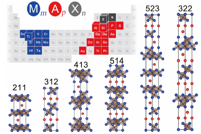
Fig. 1. Illustration of the location of the chemical elements comprising MAX phases in the periodic table, and the projection of the unit cell along <11$\bar{2}$0 > . Blue, red and black balls denote the M, A and X atoms, respectively.
With the continuous requirements and challenges of high-temperature structure materials, irradiation resistant materials, and new 2D materials, MAX phases have been one of the hot topics of ceramics for more than two decades with more than 1000 articles published. Although the application background has been changing, crystal defects are the perpetual issue because the materials development ultimately and inevitably needs the knowledge input from crystal defects. For example, the key step towards the application of MAX phases as high-temperature or even ultrahigh temperature structural materials is to make MAX compounds with excellent resistance to oxidation and mechanical degradation, and they are mainly controlled by A vacancies and basal dislocations. Understanding the crystal defects in the MAX phases could not only favor the defect engineering in MAX phases but also benefit the study of other layered structure, like MAB phases [12] and clay minerals [13]. The challenges for the study of crystal defects in MAX phases include but are not limited to the following four aspects. Firstly, there could be up to 25at.% light elements like C and N together with over 50at.% heavy transition metal elements like Nb and Ti in the crystal structure. Therefore, it is difficult to collect all the structural information in real space for all the constituent atoms by one or two techniques alone. Secondly, the solid solutes on A and X sites are usually very close to each other in the periodic table and thus are hardly distinguishable by the real-space imaging methods like high-angle annual dark-field scanning transmission electron microscopy (HAADF‒STEM). Thirdly, the vacancy configuration is unstable under electron beam irradiation [14]. Finally, the molecular dynamics simulation of dislocation-related issues is infeasible for MAX phases due to the lack of reliable atomic potential. In spite of these difficulties, the material-specific crystal defects have been extensively investigated during the exploration of MAX phases and MXenes with a synergy of desired properties. Nevertheless, there has been no systematic summary of the crystal defects in MAX phases and MXenes, although six reviews [[5], [6], [7], [8], [9], [10]] and two books [15,16] are available and some knowledge has been leveraged in the studies of MAB phases [17] and MBenes [18]. In this review, what we have known about the defects in MAX phases and MXenes are summarized. The review is organized as the following: First, we briefly introduce the unique atomically-twinned crystal structure of MAX phases. Then, the defects with different dimensions are comprehensively reviewed. After that, the defect configurations under irradiation of energetic particles are surveyed. In addition, the defects in MXenes are discussed. Finally, an outlook aimed at the future study is given.
The chemical formula of MAX phases could be generalized as MmApXn (m, p and n are integers). The MAX phases could be classified as “211” (m/p = 2, n=m‒p), “312” (m/p = 3, n=m‒p) and “413” (m/p = 4, n=m‒p) phase according to m/p. So far, more than 50 “211” phases have been discovered. There are nine “312” and “413” phases reported respectively: Ti3AlC2 [19], Ti3SiC2 [20], Ti3GeC2 [21], Ta3AlC2 [22], Ti3SnC2 [23], (V1/2Cr1/2)3AlC2 [24], Zr3AlC2 [25], (Ti1/3Cr2/3)3AlC2 [26,27], (Ti1/3Mo2/3)3AlC2 [28]; Ti4AlN3 [29,30], Ta4AlC3 [31], Nb4AlC3 [32], V4AlC3 [33,34], (V0.5Cr0.5)4AlC3 [24], (Ti3/8Cr5/8)4AlC3 [26], (Ti1/2Mo1/2)4AlC3 [35], Ti4SiC3 [36,37], Ti4GeC3 [38]. Meanwhile, some MAX phases with large m/p like (Nb1/2Ti1/2)5AlC4 [39], Ta6AlC5 [22] and Ti7SnC6 [40] have been reported. In addition, MAX phases with p = 2, like Ti5Si2C3 [36], Ti5Ge2C3 [38], Ti5Al2C3 [[41], [42], [43]], (V1/2Cr1/2)5Al2C3 [24], Ti7Al2C5 [41], Ti7Si2C5 [36,44] and Ti7Ge2C5 [38], have been observed in thin-films or bulk samples. The member of MAX phase family has been increasing as the investigation extends. Recently, Mo2Ga2C [45], Ti2Au2C [46] and Ti3Au2C2 [47] with n≠m‒p have been synthesized.
The crystal structures of MAX phases are closely related, which can be described as that the strongly bonded MmXn layers are weakly glued by p A layers along the most-closely-packed direction of MmXn layers (Fig. 1). The MmXn is stacked like their bulk counterparts in a face-cubic-center (FCC) manner except β-Ta4AlC3 [22]. For MAX phases with n=m‒p, two adjacent MmXn slabs are arranged in FCC ∑3 twin orientation with the M layer abutting A layer (Fig. 2(a)). In Mo2Ga2C, the adjacent two Mo6C octahedron layers take the twin orientation relationship as well with the mirror plane being the virtual middle plane between the two Ga layers (Fig. 2(b)). However, the strict twin orientation in Ti2Au2C and Ti3Au2C2 is destroyed with in-plane translation along the basal plane (Fig. 2(c, d)). For simplicity, only the stacking of M and A elements are considered here and designated as A/B/C and α/β/γ, respectively. The X atoms are located at the octahedral interstitial sites formed by six M atoms. Two rules could be summarized for the stacking of the closely-packed basal planes: (1) the successive three M and A layers (MMA, MAM and MAA) avoid the FCC (except for Ti2Au2C [46] and Ti3Au2C2 [47]) and head-to-head stacking (except for Mo2Ga2C [45]), meanwhile (2) MA layers should not be head-to-head stacked. Following these two rules, the stacking sequences of “211”, “312”, “413” and “523” MAX phases could be easily determined to be ABαBAβAB, ABCβCBAβABCβCBA, ABCAγACBAβABCA, and ABCβCBγBCAγACαCABαBAβABC, respectively. Breaking the rules could result in SFs, and ordered arrangement of the SFs at several unit-cell scales brings about polytypes. It is worth noting that experimentally observed failure of the rules mentioned above in thermodynamically stable MAX phases only exists in Ti3SiC2 [48] and Ti4AlN3 [49] although many modeling endeavors have been made [[50], [51], [52], [53]]. The concept of polytypism should be accepted with great caution. Because whether this kind of SFs can maintain ordered at least for several unit cells to be described with crystal structure remains unclear. Stacking errors along the normal of the closely-packed basal planes are common in the long-period ordered structure [54,55]. The only reported experimental evidence for the polytypism of Ti3SiC2 [48,49], and Ti4AlN3 [56] is high-resolution transmission electron microscopy images with only one- or two-unit cell length along [0001], and contradictory to the results of other techniques like XRD. Therefore there is no conclusive evidence to prove that those SFs could form a unique crystal structure in thermodynamically stable MAX phases.
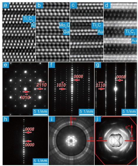
Fig. 2. Atomic-scale high-angle annual dark-field scanning transmission electron microscopy images of (a) Ti3AlC2, (b) Mo2Ga2C [
Most MAX phases (p = 1, n=m‒p) belongs to P63/mmc space group (Table 1). MAX phases with p = 2 and n=m‒p crystallize in R $\bar{3}$ m space group [43] and could be regarded as the stacking-fault-ordered phases. It is worth noting that the crystal structure of “725” phases has not been determined yet as far as we know, but the diffraction data in Ref [44]. agree with the R $\bar{3}$ m space group. Other defect-ordered MAX phases include (Zr1/3V2/3)2AlC [57], (Y1/3Mo2/3)2AlC [57], (Sc1/3W2/3)2AlC [58], (Y1/3W2/3)2AlC [58] and (Sc1/3Mo2/3)2AlC [59] (solid-solute-ordered “211” phases belonging to C2/c space group); (Ti1/3Cr2/3)3AlC2 [26,27] and (Ti1/3Mo2/3)3AlC2 [28] (solid-solute-ordered “312” phases belonging to P63/mmc space group); Nb12Al3C8 [14] and V12Al3C8 [33] (carbon-vacancy-ordered “413” phases belonging to P63/mcm space group). In addition, the recently reported MAX phases with M:A = 3:2 like Ti3Au2C2 belong to P $\bar{3}$ m1 space group [47].
Table 1 Crystal structural data of some MAX phases.
| MAX | Space group | Lattice parameters (Å) |
|---|---|---|
| Ti2AlC [7] | P63/mmc | a = 3.04, c = 13.60 |
| Ti3AlC2 [7] | P63/mmc | a = 3.08, c = 18.58 |
| Nb4AlC3 [32] | P63/mmc | a = 3.13, c = 24.12 |
| Mo2Ga2C [45] | P63/mmc | a = 3.03, c = 18.08 |
| Ti2Au2C [46] | P3¯m1 | a = 3.08, c = 54.38 |
| Ti3Au2C2 [47] | P3¯m1 | a = 3.09, c = 45.88 |
| Ti5Al2C3 [43] | R3¯m | a = 3.08, c = 48.59 |
| Nb12Al3C8 [14] | P63/mcm | a = 5.49, c = 24.01 |
| (Ti1/3Cr2/3)3AlC2 [27] | P63/mmc | a = 2.9, c = 17.81 |
| (V2/3Zr1/3)2AlC [57] | C2/c | a = 9.17, b = 5.28, c = 13.64 |
| α=γ = 90°, β = 103° |
Owing to the rapid development of transmission electron microscopy (TEM) technology in recent decades, the structural determination of MAX phases has been preferably performed by screening the candidate structures by combining the analysis of atomic-scale HAADF‒STEM images and DFT simulations [46,47]. However, the electron diffraction technique (convergent beam electron diffraction, CBED, selected area electron diffraction, SAED) is indispensable and more appropriate for the structural determination when reference structure is not available. For example, the lattice of Nb12Al3C8 could be determined to be hexagonal using the SAED patterns in Fig. 2(e-h) [14] with the following diffraction conditions: l=2n for (h $\bar{h}$ 0l) and (000l). The CBED patterns in Fig. 2(i, j) suggest that the structure has a six-fold rotation axis and two different mirrors along [0001], and one mirror perpendicular to [0001]. The point group of Nb12Al3C8 is 6/mmm. Using the diffraction conditions and point group information [60], the space group of Nb12Al3C8 is determined to be P63/mcm. Then, the atomic structure could be accurately constructed with the stacking information in the HAADF‒STEM images. It is worth noting that polarized micro-Raman spectroscopy could be used to screen or verify the crystal structure [14,61] as well.
Crystal defects can be classified as point defects (0-dimension), line defects (1-dimension) and planar defects (2-dimension) and bulk defects (3-dimension). Point defects include vacancy and solid solution atom; line defects include dislocation and disclination; planar defects include SF, grain boundary, domain boundary, etc.
The vacancies are thermodynamically equilibrium defects, which means that there always exists a certain concentration of vacancies at a given temperature. However, the concentration is normally too low to cause a noticeable change in stoichiometry. For clarity, vacancy causing the stoichiometric deviation is termed as structural vacancy nomenclaturally [62]. The vacancies in this section are structural vacancies unless otherwise specified. MX has strong ability to accommodate the structural X vacancies, which significantly impact their superconductivity [63], phase stability [[64], [65], [66]], sinterability [67], hardness [66,68], strength [69], toughness [69] and elastic modulus [68]. X vacancies are either disordered or ordered. The ordering of X vacancies gives rise to nano-domains, which could be used to tailor the mechanical properties of MX [63,[68], [69], [70], [71]]. For MAX phases, the formation energy of M vacancies (5-8 eV) is much higher than that of A and X vacancies (∼2 eV) [[72], [73], [74]]. Thus, the vacancies in MAX are predominantly formed at the A and X sites.
MAX phases have a remarkable ability to accommodate A vacancies. DFT calculations indicate that Ti2AlC can hold up to 50% Al vacancies [75]. The compositional analysis suggests that Al vacancies in Ti3Al1‒xC2 locally reach ∼50% [76]. When the concentration of Al vacancies exceeds the critical value (50% for Ti2AlC), the electrons will occupy Ti‒Al anti-bonding orbitals, demolishing the bonding between MX slabs and Al layers and destabilizing the whole structure [75]. Similar results have been reported in Ti3SiC2 [77] and Ta4AlC3 [78]. The energy barrier for the migration of A vacancies along the basal plane is less than 1 eV (0.83 eV for Ti2AlC [79], 0.9 eV for Ti3AlC2 [73]). The striking ability of Al-vacancy accommodation and migration in Ti‒Al‒C MAX phases are key to form dense Al2O3 protection layer when served at high-temperature [[80], [81], [82]].
The presence of X vacancies has been verified in Ti3AlC2-x(x≈0.20) [83], Ti4AlN3-x(x≈0.11) [29] and V4AlC3-x (x≈0.31) [33]. In fact, monolithic MAX phases could be synthesized only with a certain amount of X vacancies [83]. The formation ability of C vacancies in Ti2AlC, Ti3AlC2 and Ti3SiC2 is comparable to that of Al vacancies, roughly 2.0-3.0 eV (2.8 eV for Ti3AlC2 [73], 2.1 eV for Ti3SiC2 [73]). Nevertheless, the energy barrier for migration is 3-4 times that of Al vacancies (3.0 eV for Ti3AlC2 [79], 3.5 eV for Ti3AlC2 [73], and 3.6 eV for Ti3SiC2 [73]). Comparatively speaking, it is difficult for the migration of C vacancies. For the MAX phases with m>2, there are more than one crystallographically non-equivalent X sites, which shows different ability to accommodate X vacancies. For example, C vacancies in “413″ (Ti4AlN3-x, V4AlC3-x, etc.) are experimentally [29,33,14] and theoretically [14,84] demonstrated to be located at the 2a sites of P63/mmc space group. Basically, X vacancies in MAX are disordered, except for V4AlC3-x and Nb4AlC3-x. Etzkorn et al. reported that C vacancies in V4AlC3-x could be ordered at 1300 °C, forming V12Al3C8 [33]. Zhang et al. demonstrated that the C-vacancy-ordered phase Nb12Al3C8 is the main phase in the as-sintered bulk sample [14]. Since no superlattice diffractions have been observed in Ti4AlN3-x, the distribution of N vacancies is assumed to be random. Introducing vacancies could destabilize the hexagonal structure [77,78]. The stabilizing mechanism in V12Al3C8 and Nb12Al3C8 involves the following two aspects: occupy the 2a sites breaking only the relatively weak M—X bonds; form honeycomb networks [14].
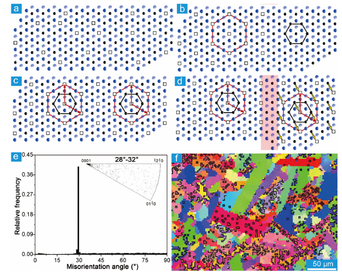
Carbon-vacancy-ordered phase is the low-temperature structure. As the temperature goes up, the contribution of configuration entropy of disorder to the free enthalpy increases, the order of vacancies decreases and even the vacancies become disordered [63]. The incomplete order-disorder transformation results in nanometer domains, like the order-disorder domain, antiphase domain, Axial domain in TiC1‒x [85] and VC1‒x [[86], [87], [88]]. The electronic and mechanical properties [89] and deformation behavior [68,90] are influenced by the amount and structure of those domains. The ordering of C vacancies and the formation of domains in Nb4AlC3‒x is illustrated in Fig. 3(a, b) and (c, d). The fault vector of the domains is determined to be 1/3< $\bar{1}$010> [14]. Domains are profuse in the as-sintered sample (Fig. 3(e, f)), whose size could be tuned by heat treatment. The sub-micrometer sized domains in the as-sintered sample were refined to be $\widetilde{2}$0 nm by annealing at 1400 °C for 30 min and fast-cooling [14].
Fig. 3. (a) Disordered carbon vacancy on (0001). Black balls and squares are carbon atoms and vacancies. Gray and blue balls represent Nb atoms above and below the carbon layer. Carbon vacancy becomes ordered on the left-hand side in (b), where the red and black hexagons outline the sub-lattice of Nb12Al3C8 and carbon-vacancy-disordered Nb4AlC3‒x. The sub-lattice of carbon vacancy on the left side and right side in (c) has no relative shifts during the ordering process. (d) The sub-lattice of carbon vacancy on the left side and right side are shifted by 1/3<$\bar{1}$010> (Nb12Al3C8 lattice), as illustrated by the yellow arrows. A domain boundary forms in the region highlighted in pink. (e) Misorientation-angle plot of as-synthesized Nb4AlC3‒x. The inset is the distribution of the rotation axis plotted in inverse pole figure. (f) Electron back-scattered diffraction orientation map. The 30°/[0001] boundaries are highlighted with black lines [
The investigation on the influence of vacancies on the properties of MAX phases is quite limited. DFT calculations indicate that A vacancies could increase the dielectric property [91], X vacancies could decrease the superconductivity transition temperature (Nb2SC1‒x [92]), whereas increase the density of state at the Fermi energy level and improve the electronic conductivity (Ta4AlC3 [78], Ti3SiC2 [77]). On the contrary, Yu et al. found that X vacancies increase ρ(T)/dT [93]. ρ(T) is the resistivity. 10%-15% X vacancies in Ti2AlN, Ti2AlC or Ti2AlC0.5N0.5 make dρ(T)/dT doubled. Zhang et al. reported that carbon vacancy and its ordering decrease the hardness and Young’s modulus of Nb4AlC3‒x [94].
Due to the structural similarity and chemical diversity of MAX phases, numerous solid solutions could be formed at M, A and X sites [96]. As the chemistry space to tailor the M site is huge (Fig. 1), solid solutions at M sites are the most intensively investigated. If M1mAXm‒1 and M2mAXm‒1 are stable, M1 and M2 can form infinite solid solution (M11‒xM2x)mAXm‒1, especially for the MAX phases with m = 2 [96], e.g., (Ti0.5V0.5)2AlC, (Ti0.5Nb0.5)2AlC, (V0.5Nb0.5)2AlC, (V0.5Nb0.5)4AlC3, etc. The doping atoms at M sites in the MAX phases with m = 2 show no chemical ordering. Dahlqvist et al. found that TM (TM = V, Ta, Nb, Cr, Mo, W) in (Ti1/2TM1/2)2AlC could take an ordered configuration at 0 K (namely some M layers are comprised of only TM without Ti), but only (Ti1/2V1/2)2AlC, (Ti1/2Ta1/2)2AlC and (Ti1/2Nb1/2)2AlC are thermodynamically stable [97]. The order-disorder transition temperature (TO‒D) for (Ti1/2TM1/2)2AlC is far lower than the synthesis temperature. Hence TM atoms are not ordered in the as-prepared sample [97]. Similar conclusions have been made for (Cr1‒xMnx)2GeC [98]. It is worth pointing out that this kind of ordered configuration could be realized at thermodynamically non-equilibrium conditions like the thin-film deposition. Recently, in-plane chemical order in (Zr1/3V2/3)2AlC, (Y1/3Mo2/3)2AlC and (Sc1/3Mo2/3)2AlC has been reported [57,59], where the difference in atomic size plays a crucial rule to keep the TO‒D much higher than the synthesis temperature [57].
For m≥3, there are less than ten stable MAX phases for each m. Even if M1mAXm‒1 or M2mAXm‒1 is not stable, M1 and M2 could still form a solid solution in a high concentration in some cases, and result in new ordered MAX phases. For example, although V3AlC2, Cr3AlC2, Cr4AlC3, Mo3AlC2 and Mo4AlC3 do not exist, (V0.5Cr0.5)4AlC3 [24], (V0.5Cr0.5)3AlC2 [24], (Ti1/3Cr2/3)3AlC2 [26], (Ti1/3Mo2/3)3AlC2 [28], (Ti3/8Cr5/8)4AlC3 [26] and (Ti1/2Mo1/2)4AlC3 [35] have been successfully synthesized. For the MAX phases with m≥3, there are multiple Wyckoff sites for M atoms. For example, M could take the 2a (0, 0, 0) and 4f (1/3, 2/3, z) of P63/mmc space group for m = 3, and the 4e (0, 0, z) and 4f (1/3, 2/3, z) for m = 4. The solid solutes are prone to occupy some specific Wyckoff sites, rather than randomly at all the possible sites. Caspi et al. found that the 2a sites in (V0.5Cr0.5)3AlC2 are completely occupied by V, 27% of the 4f sites are taken by V, and 73% by Cr [99]. Liu et al. found that Ti and Cr in (Ti1/3Cr2/3)3AlC2 are located at the 2a and 4f sites respectively [26]; similar results have been reported in (Ti1/3Mo2/3)3AlC2 [28]. For (V0.5Cr0.5)4AlC3, 32% of 4e and 84% of 4f sites are occupied by V, 68% of 4e and 16% of 4f sites are taken by Cr [99]. In (Ti1/2Mo1/2)4AlC3, 23% of 4e and 86% of 4f sites are occupied by Ti, 77% of 4e and 14% of 4f sites are taken by Mo [35]. Site preference for substitution could be observed in other non-layered structures as well [[100], [101], [102]]. DFT calculations suggest that (Ti, TM)mAlCm‒1 (n = 3, 4; TM = V, Ta, Nb, Cr, Mo, W) is stable at 0 K. The TO‒D of (Ti1/3TM2/3)3AlC2 (TM = Cr, Mo, W) and (Ti1/2M1/2)4AlC3 (TM = Mo, W) is higher than the sintering temperature ($\widetilde{1}$773 K), the ordered configuration is therefore stable. While for other (Ti, TM)mAlCm‒1, the TO‒D is far lower than the sintering temperature, thus the ordered configuration could not be formed [97]. The reason why the ordered configuration (TM occupy the sites close to Al layers) is stable includes: Ti atoms modulate the FCC stacking of TM and C; TM atoms have larger electronegativity, reducing the electrons occupying Al-Al anti-bonding states [97]. The electronegativity increases as the following order, Ti, V, Cr, and Mo, explaining well why the close-to-Al-layers 4f sites in (V0.5Cr0.5)3AlC2, (Ti1/3Cr2/3)3AlC2 and (Ti1/3Mo2/3)3AlC2, and 4e sites in (V0.5Cr0.5)4AlC3 and (Ti1/2Mo1/2)4AlC3 are mainly occupied by Cr and Mo.
The early studies on the solid solutions in MAX phases mainly focus on the improvement of mechanical properties like strength and hardness by doping [[103], [104], [105], [106], [107]]. Recently, tailoring physical properties, like thermal expansion coefficient [108], electric resistivity [93,103,109,110], magnetism [98,[111], [112], [113], [114], [115], [116], [117], [118]] and so on, attracts more attention. DFT calculations suggest that the ground state of Cr2GeC is spin non-polarized [119]. However, (Cr1-xMnx)2GeC is stable with magnetism [116]. The average magnetic moment of M sites and the Curie temperature increase with Mn concentration [112]. The Curie temperature goes up to room temperature when 20% Cr is substituted [119]. Ingason et al. demonstrated that the magnetic feature of (Cr1-xMnx)2GeC (ferromagnetic or antiferromagnetic) depends on the concentration of Mn and the atomic configuration of Cr and Mn in the lattice. The net result of the competition between ferromagnetic and antiferromagnetic relies on the local chemistry and the ordering status of M (Cr, Mn) atoms [116]. Ferromagnetic single-crystal (Cr0.75Mn0.25)2GeC thin-film has been synthesized by magnetic sputtering on MgO(111) substrate in ultrahigh vacuum. The saturate and remnant magnetic moment at 50 K is 0.36 μB and 0.031 μB per Mn atom, respectively [98]. The magnetic property of Mn2GaC is slightly better than (Cr0.75Mn0.25)2Ge: the saturate and remnant magnetic moment at 50 K is 0.3 μB and 0.15 μB per Mn atom [117] respectively, which could be further optimized by Mo substituting. The highest remnant magnetic moment was reported in (Mo0.5Mn0.5)2GaC thin-film (about 50 nm in thickness): 0.35 μB per M (Mo or Mn) at 3 K. The magnetic characteristics are also related to the competition between ferromagnetic and antiferromagnetic state [111].
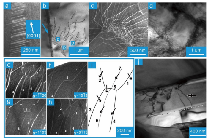
As the main plasticity carrier, dislocations play a key role in the materials strength and ductility. Knowledge about the material-specific dislocation behavior is crucial not only to understanding the mechanical response of materials but also to developing advanced structural materials [120,121]. For hexagonal close-packed (HCP) metals, basal dislocations (dislocation with a Burgers vector a) are prone to slip on the basal plane of structures with large c/a [120]. The c/a is roughly 2m for MmAXm‒1. c/a for “211”, “312” and 413 is 3.5-4.6, 5.8-6.0 and 7.7-7.8, respectively. The basal dislocations in MAX phases are more confined within the basal plane than HCP metals. Plenty of investigations at micro [122] and continuum [[123], [124], [125], [126], [127]] scale demonstrate that the dislocations in MAX phases belong to the basal slip system. These dislocations are prone to form dislocation wall [125] (Fig. 4(a)), pile up at grain boundary [128] (Fig. 4(b)). The accumulation of dislocation arrays on the basal plane could result in the bending of the basal plane. Two arrays of edge dislocations with opposite signs give rise to kink boundary [125]. The dislocation configurations in MAX phases with severe deformations are complicated. Apart from the aforementioned relatively regular dislocation configurations, there exist disorganized and entangled dislocation cells (Fig. 4(c, d)) formed by basal dislocation reaction and entanglement [124]. According to the dark-field TEM morphologies in Fig. 4(e)‒(i), the following classic dislocation reactions at the nodes are proposed: 1/3[$\bar{1}$2$\bar{1}$0]+1/3[$\bar{1}$$\bar{1}$20]→1/3[$\bar{2}$110] (the dislocation segments are 2 + 3→5, 1 + 4→5).
Fig. 4. Typical dislocation configurations in MAX phases. (a) Dislocation wall in Ti3SiC2 [
Although the elastic anisotropy along the basal plane of MAX phases is not big [130,131], the dislocations in MAX phases are prone to be the screw, 30° (the angle between Burgers vector and dislocation line), 60° and edge type, implying that dislocation lines tend to be aligned along <11$\bar{2}$0> or <10$\bar{1}$0> [131]. Gouriet et al. found that Peierls stresses of 30° and 60° full dislocations are roughly 50% higher than those of screw and edge dislocations (the Peierls stresses of the screw and edge dislocations are comparative). Therefore, the 30° and 60° dislocations are the hardest to slip, and hence most likely to be observed in TEM. Meanwhile, it is suggested that the direction preference of dislocation lines is due to the self-assembly behaviors caused by the elastic interaction between dislocations. Molecular dynamics (MD) simulation or phase field modeling is possibly better than the DFT calculation to reveal the elastic interaction and evolution of dislocation configurations [132]. Despite the lack of reliable atomic potentials, some researchers have used the first-principles MD to study MAX phases [133,134].
The plastic deformation behaviors of HCP structures like Ti, Zr, and Mg are demonstrated to be dictated by the dislocation core structure [135,136]. Recently, Gouriet et al. calculated the general stacking fault energy (γ surface) and used the Peierls-Nabarro-Galerkin model to estimate the dislocation core structure of screw, 30°, 60° and edge dislocations [131]. The analysis of the displacement of dislocation nodes caused by the structural relaxation indicates that 1/3 < 11$\bar{2}$0> type full dislocations could dissociate into two mixed 1/3 < 10$\bar{1}$0> type partial dislocations. For instance, the screw, edge, 30°, and 60° full dislocations decompose into two 30° partials, two 60° partials, a screw and a 60° partial, an edge and a 30° partial, respectively. The separating distance between two partial dislocations increases with the increase in the angle between the dislocation line and Burgers vector, but they are all calculated to be smaller than 7 Å. Theoretically, these partial dislocations cannot be observed by traditional diffraction contrast method. It is worth noting that dislocation partials at the end of the stacking fault observed by Barsoum [128] and Joulain [137] et al., as shown in the latter section, are not caused by the dissociation of full dislocations.
The critical resolved shear stress (CRSS) is a crucial factor dictating the propensity of the dislocation slip. The Peierls force of a screw, 30°, 60° and edge dislocation at 0 K is estimated to be 611, 830, 680 and 957 MPa [131]. The actual CRSS should be higher than these values. Barsoum et al. studied the deformation of highly-oriented coarse-grained Ti3SiC2 and proposed that the smallest value of CRSS of basal dislocation is $\widetilde{3}$6 MPa at room temperature and $\widetilde{2}$2 MPa at 1300 °C. Fitting the elastic hysteresis loop of MAX phases with the IKB model indicates that the CRSS of the basal dislocations is less than 100 MPa [15], which differ by one order of magnitude from those calculated by Gouriet et al. [131]. To get more accurate CRSS, the compression of MAX single-crystal sample or micrometer pillar may be needed. In recent years, much progress has been made to produce MAX single-crystal [33,[138], [139], [140]], and the millimeter-size single-crystal sample has been successfully prepared [139]. Possibly, single-crystal MAX phase sample large enough to conduct a macroscopic mechanical test to give CRSS could be produced in the near future.
It is well-acknowledged that the dislocations in the as-sintered and uniaxially-deformed MAX phases are basal dislocations belonging to basal slip or non-basal slip systems. For MAX phases, shear along non-basal plane breaks the M6X octahedrons, and hence this kind of deformation is extremely unfavorable. Zhang et al. found that the dislocations in Nb12Al3C8 are 1/3< 011-0 > type partials without any SFs bounding the partials [95]. Systematic analysis of the atomic configurations of the slipped Nb12Al3C8 along different atomic planes (Fig. 5(a-g)) suggests that only the slip by shearing Nb‒Al could produce those unconventional partial dislocations, confirming that the basal dislocations in MAX phases are produced by shearing M‒A. Meanwhile, the strain map directly demonstrates that the dislocation core lies between Nb and Al layers (Fig. 5(h)). It is worth pointing out that non-basal slips have been observed in the deformation with a slow strain rate (say 10-5/s, Fig. 4(j)) or complex stress status. It is demonstrated that the non-basal slip is a key contribution to the transformation from strain softening to strain hardening in the compression of Ti3AlC2 [129]. The non-basal slip is more obvious when the local stress is very high and stress status is complex like indentation [141]. Meanwhile, basal dislocations can cross-slip from basal plane to prismatic or the first-order pyramidal slip plane [129,142]. Guitton et al. observed non-basal dislocation segments in Ti2AlN deformed 4.5% under 350 MPa gas confining pressure [142]. Shein et al. observed not only the cross-slip of basal dislocations between the basal plane and first-order prismatic plane but also the cross-slip of a + c dislocations between the first-order and second-order pyramidal plane in the nanoindentation of Ti3SnC2. The Burgers vector ofa + cdislocation has a length of 18.9 Å. Little has been known so far about those dislocations with giant Burgers vector. The core structure and stabilizing mechanism need to be unrevealed by further experimental and simulation-related efforts.
Fig. 5. (a) Projection of the Nb12Al3C8 unit cell along < 011-0 >. (b-d), (e-g) are the atomic configurations displaced along the α and β basal plane, respectively. The displacement was introduced by shifting the part right above α or β plane with respect to the lower part by (b, e) 0, (c, g) 1/3[011-0], (d) [011-0], (f) 1/6[011-0]. (h) Atomic resolution HAADF‒STEM image of a mixed type dislocation superimposed with the strain map generated by geometric phase analysis. The Burgers circuit illustrated in (h) starts at S and ends at F, indicating a disregistry of 1/6<11$\bar{2}$0 . The inset is the εyy strain map. The figures are adapted from Ref. [
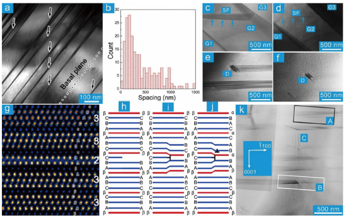
SFs are profuse in the as-sintered MAX phases, which are predominantly parallel to the basal plane (Fig. 6(a)) with a spacing 100-200 nm. Barsoum et al. found that the SFs take two morphologies in Ti3SiC2 [128], running through (Fig. 6(c, d)) or terminated within (Fig. 6(e, f)) the grain. The SF is in and out of contrast imaging with g=(0 1- 14) and g=(1 2- 10), indicating that the SF vector is 1/3 < 10 1- α> (α could not be exactly determined in the experiment. The conclusion that the faulting vector is parallel to [0001] in Ref. [128] is not correct). SFs in Ti4AlN3 are predominantly the former type [137]. Yu et al. pointed out that the SFs in Ti3SiC2 are caused by the insertion or extraction of TiC from Ti3SiC2 resembling the intrinsic or extrinsic SFs in FCC structures [143]. This argument has been confirmed in Ti4AlN3 [137] and Nb12Al3C8 [95]. Fig. 6(g) is the atomic-scale HAADF‒STEM image of Ti3AlC2. The stacking of Ti and Al in the perfect Ti3AlC2 region could be described asCBAβABCβCBA. The adjacent Ti3C2 slabs are in twin orientation, and the Al layers (β) take the same stacking as the second-nearest-neighboring Ti (B), forming Ti‒Al‒Ti prism with the two first-nearest-neighboring Ti (A). The formation of SFs does not change the relative stacking manner of Al with respect to the first and second nearest neighboring Ti layers (Fig. 6(g)). Extraction of one TiC slab results in the stackingCBAβ|BCβCBA(| denotes the position of SF) with a faulting vector R=n/8[0001] (Fig. 6(h, i)). To maintain the local stacking of Al and Ti, slips with C→B(β)→A(α)→C should occur, giving rise toCBAβ|ABαBAC, which is similar to the formation course of I1 type SFs in HCP metals [120]. The partial dislocations bounded at the end of SFs are formed and the net faulting vector is R=1/3 < 0$\bar{1}$10 > +1/8[0001] (Fig. 6(j)). The faulting vector for the extraction or insertion of n MX slabs in “312” and “413” phases is R=n/3 < 0 $\bar{1}$10 > +n/8[0001] and R=n/3 < 0$\bar{1}$10 > +n/10[0001], respectively. Structural relaxation due to the excess or depletion of MX slabs could lead to the deviation of the faulting vector along [0001] from the ideal value (n/8[0001], n/10[0001]) [95,137]. Thus, SFs running through the grain (A, Fig. 6(k)), bounded by partial dislocations (B, Fig. 6(k)) and SFs vertical to the basal plane (C, Fig. 6(k)) in Ti4AlN3 [137] could be well understood.
Fig. 6. (a) TEM morphology of SFs in Nb12Al3C8. The dotted line illustrates the basal plane. (b) Statistic histogram of the spacing between SFs. (c-f) SFs and dislocations in Ti3SiC2 [
These unique SFs, frequently observed in MAX phases, like Ti2AlC [41], V2GeC [144], Ti3AlC2 [145,146], Ti3SiC2 [143], Ti4AlN3 [137], etc., could be regarded as intergrowth structure of MX in MAX. When the intergrowth structure is at the scale of unit cell, it can be regarded as the co-growth of different MAX phases, like Ti3AlC2 and Ti2AlC [146], Ta4AlC3 and Ta6AlC5 [22,147], and Ta2AlC and Ta4AlC3 [22,147]. Periodic co-growth of “211” and “312” MAX phases at atomic scale could give rise to “523” MAX phases, like (V0.5Cr0.5)5Al2C3 [24], Ti5Ge2C3 [38], Ti5Si2C3 [36], and Ti5Al2C3 [41,42,43]. Likewise, the co-growth of “312” and “413” phases results in “725” phase, e.g., Ti7Ge2C5 [38], Ti7Si2C5 [36,44], Ti7Ge2C5 [38] and Ti7Al2C5 [41].
The misorientation of adjacent grains brings in tilt, twist, and complex grain boundary. The complex grain boundary could be considered as the combination of tilt and twist grain boundary [148,149]. Small-angle grain boundary (θ < 10°) could be described with Frank-Billy dislocation model, while large-angle grain boundary (θ > 10°) could be described with coincidence site lattice, O-lattice, DSC, etc. [120,150]. Small-angle tilt grain boundary comprises an edge dislocation wall. The tilt angle is calculated by θ=b/D (b and D is the modulus of the Burgers vector and the spacing between dislocations, respectively). Small-angle twist grain boundary are interpreted by screw dislocation networks, which could be orthogonal and more commonly hexagonal [149,151,152]. The twist angle is calculated by θ=b/($\sqrt{3}l_h$) ($l_h$ is the length of the hexagon edge).
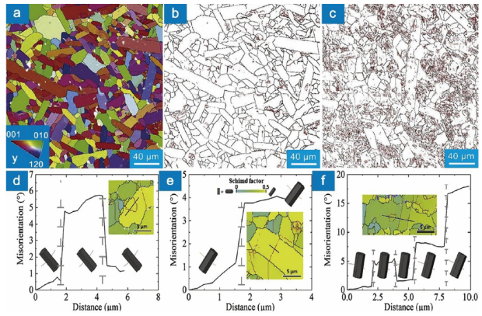
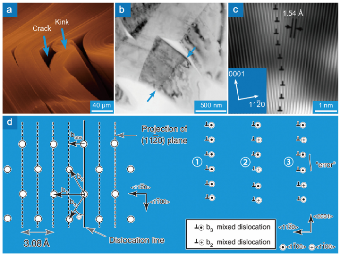
Large-angle grain boundaries prevail in the as-sintered MAX phases [153]. Benitez et al. found that the misorientation angle in Ti2AlC is predominantly larger than 10° [153], Fig. 7(a, b). After cyclic compression, profuse small-angle grain boundaries are formed in the grains with median or high Schmid factor (0.25-0.5) (Fig. 7(c-f)). The morphologies of the small-angle grain boundary could be categorized into three kinds: semi-closed loop, closed loop and straight line, Fig. 7(d-f). The semi-closed and fully-closed loops correspond to dislocation cells comprising complex dislocation configurations. While the straight lines correspond to dislocation walls. The formation of paired straight lines gives rise to kink boundaries. The knowledge regarding the first two are quite limited due to the complexity, and the available studies are concentrated on the last one. The formation of the kink is often accompanied by the formation of delamination and cracks, Fig. 8(a). With the contribution of cracks, the kink angle could be as large as 12°-60° [125]. The formation of kink boundaries gives rise to numerous sub-grains (the number of grains in the sample compressed by two cycles increases by 305%) [153]. It is worth noting that kink boundaries in MAX phases contain twist characteristics. The tilt-dominated kink boundary (about 15°) in Fig. 8(b-c) is twisted about 2° [123]. Farber et al. pointed out that the kink boundary could be explained as dislocation walls comprising mixed dislocations, Fig. 8(d). Although the dislocation wall comprising mixed dislocations with the same Burgers vectors is unstable, the wall with an alternative arrangement of mixed dislocations having opposite screw character is stable [153], Fig. 8(d). The misarrangement of those dislocations could contribute a twist angle φ=θ∙bs/(N∙be) (θ is the tilt angle, bs and be are the screw and edge character of the Burgers vector, and N is the number of misarranged dislocations).
Fig. 7. (a) Inverse pole figure map of Ti2AlC with y-axis in the vertical direction. Grain boundary maps of the as-prepared (b) and cyclically compressed sample (c). The low- and high-angle grain boundaries are marked by red and black lines, respectively. (d)‒(f) Misorientation profiles and unit cell orientations. Inserts show magnified Schmid factor maps for the corresponding grains with low- (red lines) and high-angle (black lines) grain boundaries. The figures are adapted from Ref. [
Fig. 8. (a) Scanning electron microscopy morphology of kink in Ti3SiC2 [
Different from the small-angle tilt grain boundary, small-angle twist grain boundary could be interpreted as hexagonal screw dislocation networks (HSDNs) [120,150], which have been observed in Al2O3 [152], body-centered-cubic and FCC metals [120,150,154,155]. Zhang et al. demonstrated that regular hexagonal dislocation networks are formed in Ti3AlC2 compressed at 1200 °C with a strain rate of 10-5/s, meanwhile the dislocation segments are screw type [156], Fig. 9(a). HSDNs give rise to the small-angle twist sub-grain boundaries. As the strain goes up, new dislocations react with the as-formed HSDNs, resulting in smaller HSDNs in the original HSDNs. Fig. 9(b) plots the dependence of lh and θ on the deformation. Clearly, the size of the hexagons in HSDNs decreases and the twist angle increases with the increase in strain. For the sample compressed by 26%, the twist angle is ∼0.5°. The Burgers vector of dislocation segments out of contrast in Fig. 9(d), (e) and (f) is 1/3[$\bar{1}$2$\bar{1}$0], 1/3[$\bar{1}$$\bar{1}$20], 1/3[$\bar{2}$110] (a, b and c in Fig. 9(c)). The dislocation reaction at the nodes is a+b→c. The formation of HSDNs and small-angle twist grain boundaries contributes to the work hardening of Ti3AlC2, but the influence should be quite limited due to the small twist angle.
Fig. 9. (a) A typical TEM morphology of hexagonal screw dislocation networks. (b) Strain dependence of the length of hexagon edge and twist angle. (c) Crystallographic directions of the diffraction vectors and Burgers vectors. TEM dark field images are recorded with a diffraction vector (d) g1, (e) g2 and (f) g3. Solid and dotted lines illustrate the dislocations in and out of contrast, respectively. White arrows denote the Burgers vectors of the dislocation segments out of contrast. The figures are adapted from Ref. [
Amorphous films of several nanometers in thickness ubiquitously exist at the grain boundary in ceramics (like Si3N4 and Al2O3), which could dramatically deteriorate the mechanical performance at high-temperature [158,159]. Fortunately, amorphous films are absent in the sintered MAX [7,143,146,[160], [161], [162]]. Another impact of grain boundary on the mechanical properties is known as the grain size effect. The grain shape is concomitantly changed as the grain size of MAX phases is altered. For example, small grains take a near-equiaxial morphology while the coarse grains are plate-like. Systematic investigations on the grain size effect are therefore not available so far. According to the Hall‒Petch paradigm, MAX phases with smaller grains are stronger. El-Raghy et al. [163] found that, for the Ti3SiC2 sample with 3-5 μm grains, the fracture strength is 1050 MPa for compression and 600 MPa for bending, and the yield strength at 1300 °C is 500 MPa, while those values for the sample with 100-200 μm grains are 720, 330 and 320 MPa. Similar results were observed in Ti2AlC and Ti2AlN [105]. The coarse-grained sample has lower strength but higher fracture toughness [164], better resistance to thermal shock [163] and superior damping performance [165].
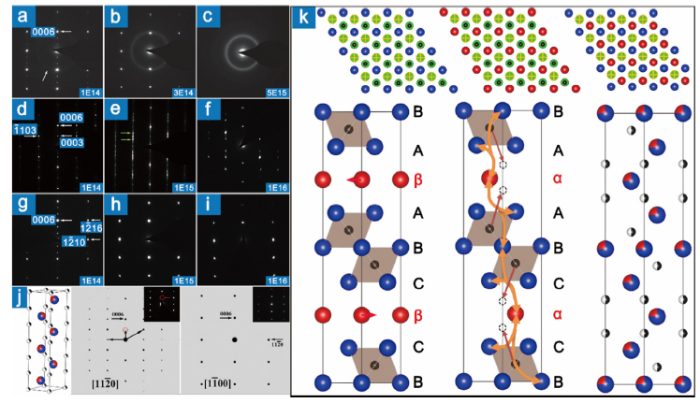
Irradiation of materials by electrons, neutrons or ions could create various types of defects, including point defects, dislocation loops, SFs, and even voids. Extensive accumulation of those defects could result in order-disorder transformations and even amorphization, which dramatically degrades the physical, chemical, electrical and catalytic properties. Most MAX phases have superior resistance to irradiation of neutron [166], Ar [167], He [168,169], Xe [[169], [170], [171], [172], [173]], Kr [[169], [170], [171], [172], [173]], Au [169,174,175], and I [176] ions. For example, atomic disorder in Ti3(Al0.5Si0.5)C2 occurs with 0.15 dpa irradiation of 2 MeV Xe ions, but no amorphization could be detected up to 6.67 dpa [172]. Under the irradiation of He ions, Ti3AlC2 remains crystalline up to 52 dpa [168]. Ti3AlC2 and Ti3SiC2 are amorphous-resistant up to 25 dpa irradiation of 1 MeV Ke and Xe ions [170]. However, Cr-containing MAX phases show poor irradiation resistance. Under the irradiation of 340 keV Xe2+, the amorphization starts at 1.6 dpa for Cr2AlC and 0.27 dpa for Cr2GeC, and completes at 2.7 dpa and 0.81 dpa, respectively [177]. Fig. 10(a-c) shows the amorphization of Cr2AlC under the irradiation of 1 MeV Au ions. Clear amorphization rings are observed in the SAED patterns at 1 × 1014 cm-2 and Cr2AlC is completely amorphized at 1 × 1016 cm‒2 [178].
Fig. 10. SAED patterns along of (a-c) Cr2AlC [
At low dose stage, a great number of point defects, especially the antisite defects are produced [179]. The minimum threshold displacement energy for the C, Si and Ti in Ti3SiC2 is 7, 26 and 23 eV, respectively [180], and the most energetically favorable antisite defects are MA‒AM pairs (Table 2). The MA antisites can migrate via the neighbor A vacancies (energy barriers are 0.3 and 0.6 eV in Ti3SiC2 and Ti3AlC2 [73]). With the accumulation of antisite defects, M and A atoms statistically co-occupy the cation sites [181], the atomic structure of MAX phases is restructured with the redistribution of X atoms [182], forming a new HCP structure with M and A co-occupying the cation sites. The co-occupancy of M and A atoms was first proposed by the combination analysis of experimental and simulated HRTEM images, and has been confirmed by HAADF‒STEM images recently [181]. Fig. 10(d-f) and (g-i) present the SAED patterns along <11$\bar{2}$0> and <10$\bar{1}$0> of Ti2AlN [182]. The (000l) and (1$\bar{1}$0l) diffraction spots with l = 3n±1, 3n±2, and (1$\bar{2}$1l) diffraction spots with l = 6n±2 become weaker or even disappear compared to the SAED patterns of the virgin sample as the irradiation proceeds. It is demonstrated that the changes in SAED patterns are caused by the formation of a new HCP structure, (Ti2/3Al1/3)3N, where Ti and Al atoms co-occupy the Ti and Al sites, and N atoms partially migrate to the intestinal sites of Ti‒Al‒Ti prism in the original structure, Fig. 10(j). This HCP structure is first observed in the crystallization process of Cr‒Al‒C amorphous coatings [183,184]. Another feature is that the HCP (Ti2/3Al1/3)3N transforms to an FCC structure as the irradiation flux increases (Fig. 10(f, i)). The HCP→FCC structural phase transformation has been observed in Ti2AlC [174], Cr2AlC [177], Ti2AlN [182], V2AlC [178], Ti3AlC2 [179], Ti3SiC2 [173] and Ti4AlN3 [182]. For MAX phases with m≥3 (like “312” and “413”), there are two possible low-energy sites for A, as shown in the up three illustrations in Fig. 10(k). It is reported that the Al atoms in Ti3AlC2 will migrate from the 2b (upper middle configuration) to 2d (upper right configuration) sites during the irradiation [179], leading to the polytypic transformation from BCβCBAβAB to BCαCBAβAB, bottom left and middle illustrations in Fig. 10(k). The energy penalty for the polytypic transformation caused by the migration of A element to the nearest potential valley is 0.70 eV for Ti3SiC2 [53], 1.20 eV for Ta4AlC3 [52], 0.32 eV for Ti4GaC3 [185] and 1.22 eV for Nb4AlC3 [51]. The transformation barrier is 0.86 eV (in Ti4GaC3) [185]. The small energy required for the polytypic transformation could be easily provided by the hundreds-KeV irradiation of heavy ions. The remaining process is the same to that in “211” phases, TiAl and AlTi form uniformly accompanied by the re-distribution of C among all octahedral interstitial sites formed by six Ti(Al) atoms, bottom middle and right illustrations in Fig. 10(k).
Table 2 Formation energy of antisite pairs.
| Ti3SiC2 | Ti3AlC2 | Cr2AlC | Cr2GeC | Ti2AlC | Ti2AlN | |
|---|---|---|---|---|---|---|
| MX‒XM | 11.67 [186] | 11.40 [186] | 7.53 [186] | 6.44 [186] | 11.78 [186] | 11.71 [186] |
| 6.90 [73] | 6.20 [73] | |||||
| AX‒XA | 6.05 [186] | 8.41 [186] | 8.86 [186] | 5.71 [186] | 9.41 [186] | 10.57 [186] |
| 3.30 [73] | 4.60 [73] | |||||
| MA‒AM | 3.52 [186] | 3.13 [186] | 2.40 [186] | 4.04 [186] | 2.96 [186] | 2.52 [186] |
| 2.50 [73] | 1.60 [73] |
It is found that high-order MAX phases (with larger m) show better resistance to structural damage than low-order MAX phases counterparts (with the same constituent elements but smaller m) [182]. For example, at a fluence of 1 × 1015 cm2, Ti4AlN3 basically retains its structure, while appreciable amounts of Ti2AlN transform to the FCC structure under the irradiation of 1 MeV Au+. Exposed at 2 × 1016 cm2, there remains a considerable amount of the HCP structure in Ti4AlN3, while the HCP structure is completely transformed to the FCC structure in Ti2AlN. The structural transition involves three aspects: (1) polytypic transformation (for MAX phases with m≥3); (2) formation of MA and AM antisite defects with breaking the M—X and M—A bonds; (3) redistribution and uniformation of X vacancies. The sequences of those processes are unclear so far. The proportion of Ti—N bonds in Ti4AlN3 (0.15/Å3) is ∼40% higher than that in Ti2AlN (0.11/Å3). Meanwhile, Ti—Al bonds in Ti4AlN3 (0.066/Å3) is only half that in Ti2AlN (0.11/Å3). Since the Ti‒N is much stronger than Ti‒Al, it is not unexpected that Ti4AlN3 shows superior structural stability to Ti2AlN under irradiation.
It is worth noting that the accumulation of point defects could result in dislocations as well. The dislocation loops in Ti2AlC irradiated at 360 and 695 °C are around 15 and 51 nm, respectively, and predominantly confined in the basal plane [166].
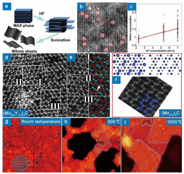
Chemically etching off A elements from the MAX phases could produce new 2D materials known as MXenes [187,188] (Fig. 11(a)), which have been used as electromagnetic interference shielding [189], molecular sieving [190], catalyst [191], photo-absorber [192], biosensor [193], electrochemical energy storage materials [[194], [195], [196]] and laser technology [197].
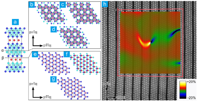
Fig. 11. (a) Illustration of the typical process from MAX phases to MXenes [
Generally, the point defects regarding M and X sites in MAX phases are inherited in MXenes [58,[198], [199], [200], [201], [202], [203]]. Yang et al. reported that doping 20% Zr and Ti at Nb sites in Nb4C3Tx slightly lowers the capacity of supercapacitor [199]. Doping Ta and W at Nb sites is demonstrated to degrade the electrochemical performance of Nb4C3Tx [204]. Zhou et al. found that substitution of Ti at V sites in V2CTx significantly improves the exfoliability and the electrochemical performance [205]. Carbon vacancies are promising and effective electrocatalysts for hydrogen evolution reaction by water splitting [206] and could improve the electronic conduction and flexibility of MXenes [202]. Doping heteroatoms at carbon vacancies is also a promising way to tailor physicochemical properties of MXenes. For example, the band gap of Sc2CF2 MXene monolayer can be modified through C substitution by Si, Ge, Sn, F, S, N, and B [207]. Doping N in MXenes has been experimentally conducted and proven to be beneficial for energy storage [208,209].
Here, we focus on the M vacancies which are not available in MAX phases and produced by the etching process or electron irradiation. It is demonstrated that there are a great number of Ti vacancies in Ti3C2Tx MXene (Fig. 11(b)), which are caused by the etching of HF aqueous solution and mainly form on the two surface sublayers and could be tuned by HF concentration [210,211], Fig. 11(c). The vacancy concentration in Ti3C2Tx MXene etched by 7 wt.% HF aqueous solution is estimated to be smaller than 3%. High concentration structural M vacancies could be generated by selectively etching off M1 (or M2) and A from the MAX phases with two M elements, (M1, M2)mAXm‒1. For example, most Al and Sc atoms are etched off by immersing (Nb2/3Sc1/3)2AlC powders in 48 wt.% HF aqueous solutions for 30 h, resulting in Nb4/3CTx (Tx representing functional groups) MXene with 2/3 randomly distributed M vacancies [200]. The M vacancies are not necessarily disordered, whose distribution depends on the distribution status of solution atoms in the original MAX phases. In solution-atom-ordered (W2/3Sc1/3)2AlC [58], (W2/3Y1/3)2AlC [58], (Mo2/3Y1/3)2AlC [57,212] and (Mo2/3Sc1/3)2AlC [59], Y/Sc are ordered in the basal plane. By selectively etching off Al and Sc/Y atoms, ordered M vacancies are produced, Fig. 11(d-f), resulting in unique atomic patterns (Fig. 11(f)). It is worth mentioning that the conduction and capacitance of Mo4/3CTx with ordered Mo vacancies are superior to Mo2CTx [59]. Very recently, Mo vacancies in Mo2TiC2Tx MXene have been used to immobilize Pt atoms, enhancing the catalytic activity for the hydrogen evolution reaction [213]. M adatoms are another common crystal defect in MXenes. It is estimated that 75% of the surface of fresh Nb2CTx MXene is covered by Nb adatoms, which is proposed to be adsorbed on the Nb2CTx surfaces during the etching process [214]. Ti and C adatoms could be formed on the Ti surface of Ti3C2 under electron beam irradiation at high temperature (>500 °C), where the free Ti and C atoms are from the neighbouring Ti3C2 substrate by forming holes, and the Ti surface is formed by the removal of Tx of Ti3C2Tx MXene, Fig. 11(g, h). Sustained formation of Ti and C adatoms facilitated by Ti-vacancy-clusters promotes the growth of new 2D “TiC” layers on the de-functionalized Ti3C2Tx, resulting in the formation of Ti4C3 and Ti5C4 domains [215], Fig. 11(h, i).
This review systematically summarizes what has been known about the crystal defects with different dimensions. The defect characters, distribution status and influence on the properties are elaborated regarding the vacancies and solid solutes. Meanwhile, the structural features and implications for the properties of dislocations, stacking faults, domains and grain boundaries are surveyed. Finally, the crystal defects in irradiated and A-etched-off (MXene) MAX phases are reviewed. One thread of the development of materials science is finding out the character of crystal defects and their impacts on the properties to realize the defect engineering, and to precisely tailor the materials at various length scale. For MAX phases and MXenes, we are still far away towards this end, and more work are needed in the various aspects. For example: (1) the mechanism of defect ordering and its implication on properties; (2) the influences of crystal defects on the exfoliation of MAX to produce MXene; (3) the impacts of crystal defects on the irradiation resistance; (4) the atomic-scale structure of the grain boundary and domain boundary; (5) the dislocation core structure and its role in the deformation behavior; (6) the quantitative description of plastic deformation using continuum crystal plasticity model and dislocation theory.

 WeChat
/
| 〈 |
|
〉 |