Search for articles:
Mingshi Yu
Corresponding authors:
Received: 2019-04-8
Revised: 2019-05-7
Accepted: 2019-06-4
Online: 2020-01-15
Copyright: 2020 Editorial board of Journal of Materials Science & Technology Copyright reserved, Editorial board of Journal of Materials Science & Technology
More
Abstract
Oxide/metal/oxide (OMO) and its derivatives are considered as the promising alternatives to achieve high performance transparent electrodes (TEs). The percolation thickness and conductivity of the metal layer are very crucial for the optoelectrical properties of any OMO TE. Here, we report a facile method to promote the initial growth of the metal layer by improving the interfacial wettability between O-M interface. By subsequently combined with high-quality zinc oxide (ZnO) films, ZnO/Cu/ZnO TEs that have not only low sheet resistance (19.3 Ω/sq) but also enhanced thermal stability can be obtained, with a performance of an average transmittance of 84.4% over the visible spectral range of 400-800 nm.
Keywords:
Transparent electrodes (TEs), as essential components of optoelectronic devices, have been widely used in many products, including solar cells [1], organic light-emitting diodes (OLEDs) [2], flat panel displays [3] and touchscreens [4]. Indium tin oxide (ITO) has a high conductivity and transparency in the visible spectrum. It is widely used as transparent electrode materials in modern optoelectronic devices [5]. However, the scarcity of indium element leads to a high cost, and fragile due to poor mechanical ductility. Researchers have been committed to finding TE materials that can alternative ITO. The current researches are mainly focused on carbon nanotubes [6], graphene [7], metal nanowires [[8],[9]] and ultrathin metal films [[10], [11], [12]]. Among them, structural configuration represented by oxide/metal/oxide (O/M/O) and its derivatives are considered as one of the promising ways to achieve high performance TEs. Compared with traditional ITO, the ductility of metal films ensures the ability to deform on polymer substrates [13]. In addition, the metal film structure sandwiched between the bottom and top oxide films can effectively prevent chemical corrosion. ZnO is a semiconductor material commonly used in photovoltaic devices with a wide-bandgap (3.37 eV) and high optical transparency in the visible spectrum. Furthermore, mechanical stability and abundant amount of raw materials can also be considered as part of its advantages. At present, the preparation methods include chemical vapor deposition, sol-gel method, electron beam evaporation and magnetron sputtering deposition [[14], [15], [16], [17]].
Some coinage metals (i.e., Ag, Au, and Cu) are often chosen as metal layers in O/M/O structures because of their excellent electrical conductivity. It is generally accepted that the growth mode of these noble metals on heterogeneous substrates is a three-dimensional (3D)-island (or Volmer - Weber) growth and can be divided into the following four stages: (i) in the early nucleation stage, formed small and discrete 3D granules on the heterogeneous surface, (ii) coalescence behavior between discrete metal clusters, (iii) formation of a metal nanonetwork near the penetration threshold thickness, (iv) a continuous metal film formed with thickness increases. As a result, for metal films, a compromise between optical transmittance and conductivity is inevitable. Therefore, the realization of a completely continuous and smooth metal film with an ultrathin thickness is considered as an effective method [18]. At present, some methods are employed to improve the quality of ultrathin metal films, mainly including oxide seed layer [[19],[20]], heterogeneous metal seeding [[21],[22]] and gas additives [[23], [24], [25], [26]]. The above-mentioned methods are believed to provide dense nucleation sites that inhibit the growth of the initial 3-dimentional islands during the early nucleation stages.
Directly oxidizing Cu as a wetting layer (denoted as Cu(O)Cu) can improve the growth quality of metal layers in O/M/O structures, but the precisely control of the introduction amount and time of oxygen is quite cumbersome to real process: any slight changes may result in the unstable yielding. In this paper, we adopt a simple and facile UV irradiation method to treat the interface between-in M/O, without introducing other substances, and found out that the interfacial wettability can be greatly enhanced, which in turn promotes the crystallization and growth of the ultrathin metal layer. The prepared ZnO/Cu/ZnO (ZCZ) sandwiched transparent electrodes exhibit excellent photoelectric properties surpassing the performance of ZCZ electrodes without any further post-treatments.
The Z/C/Z multilayer structure was fabricated on glass substrate at room temperature using a two-chamber magnetron sputtering system (No. JGP-450). First, glass substrates (having a thickness of 0.5 mm and an area of 1 inch × 1 inch) were ultrasonically washed in deionized water, acetone, ethanol and deionized water for 10 min, respectively. Then the substrate was dried in an oven for use. The sputtering chamber was evacuated to a base pressure of 2 × 10⁻⁴ Pa, and the flow rate of Argon gas (99.999%) was fixed at 40 sccm during the deposition of ZnO and Cu. An ZnO target (99.999%) was used for depositing ZnO films with work pressure of 0.7-2.0 Pa and RF power of 100 W. The ZnO target was pre-sputtered for 5 min to remove any surface contamination. Cu layer was deposited from a Cu target (99.999%) with DC power of 50 W and working pressure of 0.6 Pa. In order to improve interfacial wettability in Cu/ZnO, UV treatment was performed 2 min before Cu deposition. The film thickness was controlled by changing the sputtering time, which was calibrated via cross-sectional thickness evaluation.
The basic preparation procedures are the same as that of ZCZ TEs, except that after the deposition of the bottom ZnO, 1 nm of Cu was sputtered and then heat-annealed for a period of time to oxidize the Cu film.
The crystal structures were characterized with X-ray diffraction (XRD). The transmittance spectra of the Z/C/Z TEs were determined using ultraviolet-visible spectrometer (UV-5200PC), and a four-probe measurement system was used to measure sheet resistance of the films. The sheet resistance of the TCs was averaged over at least five different measurements for each sample. The cross-section morphology of the films was characterized by scanning electron microscopy (SEM).
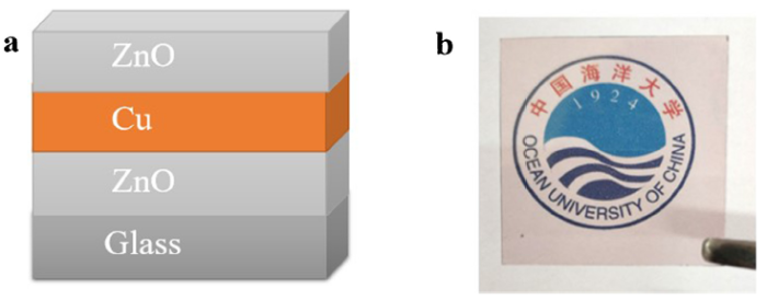
Fig. 1(a) is a schematic diagram of transparent electrodes fabricated by an ultrathin Cu film sandwiched between two layers of ZnO on a glass substrate. Fig. 1(b) is the typical picture of the transparent electrode based on ZnO/Cu/ZnO, from which it can be clearly seen that the prepared electrode has high transparency.
Fig. 1. Schematic drawing of the ZnO/Cu/ZnO transparent electrodes (TEs) on a glass substrate (a) and (b) an optical photograph of a transparent electrode based on ZnO/Cu/ZnO.
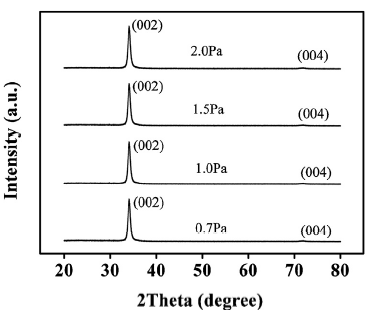
Fig. 2 shows the XRD patterns at different deposition pressures. No extra peaks due to impurity were observed by XRD test, and the high intensity and sharpness of diffraction peaks indicate that the prepared films have good crystallinity [[27], [28], [29]]. For all the samples, only the ZnO (002) and ZnO (004) peaks were observed, Moreover, the intensity of the (002) peak appered to be much stronger than the (004) peak for each sample. From the XRD patterns, it can be found that all the films exhibit preferential orientation with c-axis perpendicular to the substrate surface [30]. In addition, the crystallization quality of ZnO films can be evaluated by peak strength and full width of half maximum (FWHM), which will be discussed later in the paper.
Fig. 2. XRD patterns of ZnO films with different deposition pressures.
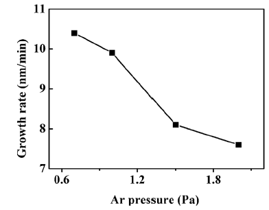
Fig. 3 shows the relationship between the growth rate and deposition pressure. It is found that the growth rate decreases from 10.4 to 7.7 nm/min when the deposition pressure increases from 0.7 to 2.0 Pa. This might be the result of the increased mean free path of the sputtered particles at a lower deposition pressure.
Fig. 3. Dependence of growth rate on the sputtering Ar pressure.
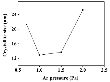
The mean crystallite sizes were calculated from the FWHM of the (002) diffraction peaks (Table 1) using the Debye-Scherrer formula [31]:
$D=\frac{0.9\lambda}{\beta cos\theta}$ (1)
Table 1 Parameters of the ZnO samples estimated from XRD patterns.
| Ar pressure (Pa) | FWHM (°) | Lattice constant (nm) | Stress, σ (GPa) |
|---|---|---|---|
| 0.7 | 0.39 | 0.524 | -1.62 |
| 1.0 | 0.64 | 0.530 | -4.23 |
| 1.5 | 0.61 | 0.526 | -2.52 |
| 2.0 | 0.33 | 0.522 | -0.61 |
In the above formula, D, λ, β and θ respectively represent the mean crystallite size, X-ray wavelength (1.5418 Å), FWHM in radians and Bragg's diffraction angle. From Fig. 4 and Table 1, we can observe that increasing the Ar pressure from 0.7 to 1.0 Pa leads to a decrease in the crystallite size and an increase in the FWHM value. When the Ar pressure is gradually increased from 1.0 to 2.0 Pa, the crystallite size increases and the FWHM value decreases. This implies that the crystallinity of the films initially deteriorates as the Ar pressure increases from 0.7 to 1.0 Pa and then improve from 1.5 Pa.
Fig. 4. Dependence of the crystallite size on the deposition pressure for ZnO films.
To further understand the effect of the Ar pressure on the stress of ZnO films, the estimated values of the stress in ZnO film are summarized in Table 1. We calculated the stress in the films by using the following formula [32], which is valid for hexagonal lattice.
$\sigma_{film}=\frac{2c_{13}^{2}-c_{33}(c_{11}+c_{2})}{2c_{13}}\frac{c_{film}-c_{bulk}}{c_{bulk}}$ (2)
In the above formula, cbulk (0.5205 nm) is the strain-free lattice constant, cfilm is the lattice parameter of the ZnO films measured by XRD [33] and can be calculated by the Bragg formula:
$2d sin\theta=n\lambda$ (3)
The elastic constant cij of single crystalline ZnO can be used as c11 = 208.8, c33 = 213.8 and c12 = 119.7, c13 = 104.2, ε= (cfilm-cbulk)/cbulk. This yields the following numerical equation for the stress derived from XRD:
$\sigma_{film}=-233\times \varepsilon(GPa)$ (4)
Table 1 shows the FWHM, lattice constant and calculated stress (The negative sign shows that the films are in a state of tensile stress) using the above equations for different Ar pressures.
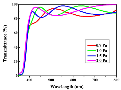
Fig. 5 shows the optical transmittance spectrum of ZnO thin films as a function of deposition pressure, in the wavelength range of 350-800 nm. As the deposition pressure increases, the transmittance in the visible range increases slightly, whereas the average transmittance in the range of 400-800 nm is above 85% for all the films. All films have a thickness of around 300 nm. In fact, the optical properties of ZnO thin film can also be further effected by doping and low-temperature annealing, as investigated in Ref. [34].
Fig. 5. Optical transmittance as a function of wavelength for ZnO films with different deposition pressures.
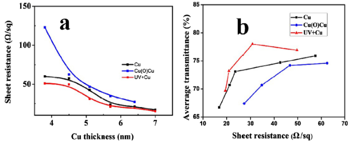
Fig. 6(a) shows the sheet resistance change with the thickness of the Cu layer on the aforementioned ZnO films under different treatment conditions: (1) direct deposition of Cu layer (denoted as Cu), (2) directly oxidizing Cu as a wetting layer (denoted as Cu(O)Cu), and (3) UV treatment of the ZnO surface before Cu deposition (denoted as UV + Cu). All the sheet resistances for these films decrease rapidly as the thickness of the metal layer increases, among with the sheet resistance curve of UV + Cu film shows the lowest position in the figure, exhibiting an improved conductivity regarding to the same metal layer thickness. This phenomenon should be closely related to the wettability of metal-oxide interface, which would be further confirmed in this article later on. We found that at the same thickness, the sheet resistance of the Cu(O)Cu layer is even larger than that of the pure Cu film. We believe that this could be due to the presence of some oxidized CuOx phases in the layer, which would affect the electrical conductivity. As we above-mentioned, the precise control of the introduction amount and time of oxygen is quite cumbersome to real process for this Cu(O)Cu layer. The average transmittance of the UV + Cu film is 73.9% in the visible spectrum range, and the sheet resistance is 20 Ω/sq, whereas the Cu film exhibited an optimal average transmittance of 73.1% in the same spectral range, and the sheet resistance is 26 Ω/sq (Fig. 6(b)). The optoelectrical performance of the Cu(O)Cu layer is even worse due to the above reasons.
Fig. 6. Optoelectrical properties of ultrathin Cu films on ZnO films under different treatment conditions. (a) Change in the sheet resistance of the films as a function of Cu thickness. (b) Average transmittance in the spectral range of 400 - 800 nm versus the sheet resistance for the films.
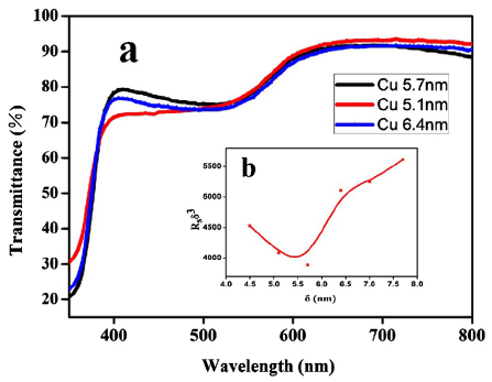
Fig. 7(a) and Table 2 show the sheet resistance and the total transmittance of the ZCZ TEs in the visible spectrum range. The highest transmittance of ZCZ TEs was obtained by using 5.7 nm UV + Cu layer. It is generally accepted that the sheet resistance will continue to decrease as the thickness of the metal film increases. In contrast, the optical transmittance increases with the increase of thickness of the metal film before the percolation threshold of the metal film, and the highest optical transmittance is achieved near the percolation threshold. This is attributed to the inherent Volmer-Weber growth mode of metal film. Before the percolation threshold, the metal morphologies are mainly composed of discontinuous and granular metal clusters, which seriously affects the transmittance of incident light. Therefore, the main research to improve the transmittance of ZCZ TEs is by obtaining continuous metal films at a minimum thickness, so the transparency of the electrodes can be maximized by adjusting the thickness of the metal film [35]. In this paper, by plotting RSδ3 vs δ (where δ stands for the Cu film thickness), the percolation threshold of the Cu film is estimated, that is, the thickness corresponding to which the film changes from an island distribution to a continuous layer. As shown in the inset Fig. 7(b), the percolation thickness for the Cu films is found to be in the thickness about 5.6 nm. This result is quite consistent with the highest transmittance of the ZCZ TE when using 5.7 nm UV + Cu layer in Fig. 7.
Fig. 7. Optoelectrical properties of transparent electrodes based on ZnO/Cu/ZnO (a) Change in the transmittance spectra of ZnO/Cu/ZnO TEs with different Cu film thicknesses. (b) The inset is RSδ3 versus δ for determination of percolation threshold.
Table 2 Parameters of the electrode photoelectric performance.
| Cu thickness (nm) | Sheet resistance (Ω/sq) | Transmittance(%) | FOM=T10/R (×10-3 Ω-1) |
|---|---|---|---|
| 5.1 | 25.7 | 84.2 | 6.97 |
| 5.7 | 19.3 | 84.4 | 9.5 |
| 6.4 | 17.0 | 82.8 | 8.9 |
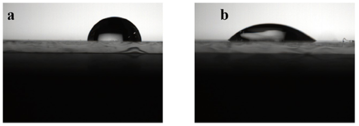
In order to reveal the phenomenon that UV treatment can improve the interfacial wettability and in return reduce the percolation threshold of Cu films, we performed an investigation by measuring the contact angles of deionized water on the surface of the ZnO films. For the ZnO film, the initial contact angle of deionized water droplets is 51°, After UV treatment, the contact angle decreases to 19°, as shown in Fig. 8. The result shows that UV treatment can increase the wettability of ZnO surface, which could play a vital role in the subsequent deposition of Cu films.
Fig. 8. Change in the contact angle of water on the ZnO film (a) without and (b) with UV treatment.
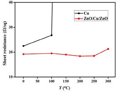
Fig. 9 shows the thermal stability of Z/C/Z TEs. The samples were first heated to different temperatures at the same heating rate, keeping for the same period of time, and then the corresponding sheet resistances were recorded after cooling down to room temperature. It can be seen from Fig. 9 that the ZCZ films still maintain excellent stability at high temperature of 300 ℃, while the sheet resistance of the Cu films without ZnO capping layer increases drastically at 150 ℃. This indicates that the Cu films have been oxidized and lost its conductivity at this temperature. The experimental results show that the ZCZ TEs have excellent thermal stability under the protection of ZnO layer.
Fig. 9. Thermal stability for only Cu film and ZnO/Cu/ZnO film, respectively.
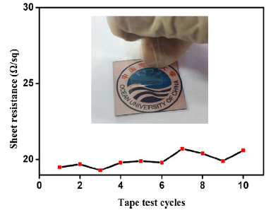
As shown in Fig. 10, the film can withstand repeated tape testing without peeling off from the substrate, indicating a good adhesion to the glass. In addition, changes in the sheet resistance of the film as a function of tape test cycles were also recorded. After 10 cycles of tape testing, the changes of sheet resistance of the films are still very small, which indicates that the films prepared possess good reliability and adhesion with glass substrates.
Fig. 10. Tape adhesion test of the ZnO/Cu/ZnO film.The inset is a typical picture of tape adhesion test.
We designed a method to fabricate ZnO/Cu/ZnO transparent conductors with high transparency and low sheet resistance. By introducing a UV pretreatment, the initial growth of the metal layer has been greatly promoted, and the interfacial wettability between O-M interface was improved notably. This facile approach can avoid the cumbersome process to directly oxidize the metal layer, further enhancing the initial nucleation density. By subsequently combined with high-quality zinc oxide (ZnO) films, ZnO/Cu/ZnO TEs that not only have low sheet resistance (19.3 Ω/sq) but also enhance thermal stability can be obtained, with a performance of an average transmittance of 84.4% over the visible spectral range of 400-800 nm.
This work was supported financially by the “youth talent project” of OUC.

 WeChat
/
| 〈 |
|
〉 |