Search for articles:
Linxing Meng, Wei Tian, Fangli Wu, Fengren Cao, Liang Li
Corresponding authors:
Received: 2018-04-26
Revised: 2018-05-24
Accepted: 2018-05-25
Online: 2019-08-05
Copyright: 2019 Editorial board of Journal of Materials Science & Technology Copyright reserved, Editorial board of Journal of Materials Science & Technology
More
Abstract
Bismuth vanadate (BiVO4) is a promising photoanode material owing to the narrow bandgap, appropriate band position, and excellent resistance against photocorrosion, however, the performance of photoelectrochemical (PEC) water splitting is largely limited by the poor carrier separation and transport ability. To address these issues, for the first time, we fabricate BiVO4 film/CuO nanocone p-n junctions as photoanodes by combing a facile spin-coating process and water bath reaction. This structure strengthens the light harvesting and promotes the charge separation and transport ability. The surface defects states are passivated by coating conformally ultrathin TiO2 onto CuO surface through atomic layer deposition (ALD) technique. Benefiting from the favorable morphology, energy band, and surface treatment, the BiVO4/CuO/TiO2 heterojunction generates an improved photocurrent that is much higher than pure BiVO4. The detailed mechanism investigations indicate that the synergetic optimization of charge separation and injection efficiency in the bulk and surface of photoelectrodes can significantly improve the performance of PEC cells.
Keywords:
Photoelectrochemical (PEC) water splitting has aroused great interest for hydrogen evolution from water by exploiting solar energy, which is regarded as one of the most efficient strategies to address the world energy crisis and environmental issues [[1], [2], [3]]. In the last few years, tremendous effort has been paid to develop highly efficient photoelectrodes to facilitate the practical application of PEC water splitting. Among the photoanode materials, bismuth vanadate (BiVO4) with monoclinic sheetlite structure has emerged as a promising material for PEC water splitting [[4], [5], [6]]. BiVO4 has a band gap of 2.4 eV, which enables light absorption up to 11% of the solar spectrum compared to 4% for the commonly used TiO2. The conduction band (CB) edge of BiVO4 lies above the thermodynamic level for H2 evolution, making the water splitting reaction easier to occur at a low overpotential. In addition, BiVO4 is composed of inexpensive elements and possesses excellent stability against photocorrosion. However, it suffers from the poor carrier separation ability, slack oxygen evolution reaction at the interface, as well as inferior transport efficiency of surface carriers. These disadvantages strictly limit its overall PEC performance.
Various strategies, including elements doping and cocatalysts loading, have been investigated to alleviate these limitations. For example, metal ions doping improved the electrical conductivity of BiVO4, yielding higher PEC activity [7,8]. Choi et al. fabricated nanoporous BiVO4 electrodes and added dual-layer oxygen evolution catalysts on the surface, which created a more favorable Helmholtz layer potential drop at the oxygen evolution catalyst (OEC)/electrolyte junction and reduced interface recombination [9]. Rao's group fabricated an amorphous Co-La double hydroxide decorated BiVO4 by plating electrodeposition, which exhibited better stability and activity for oxygen evolution reaction (OER) [10]. Sun et al. utilized novel surface-modified molecular Co3O4 catalysts to improve PEC performance of BiVO4 photoanodes [11]. Apart from the above-mentioned methods, the heterojunctions formed by combing BiVO4 with other semiconductors, including g-C3N4 [12], TiO2/BiVO4 [13], BiFeO3/BiVO4 [14], and WO3/BiVO4 [15], can also improve charge separation and transfer efficiency, owing to the internal built-in electric field at the interface. In particular, the p-n heterojunctions are expected to have better performance compared to the n-n homojunctions, due to its stronger internal electric field. As a typical p-type semiconductor with narrow band gap between 1.21 and 1.4 eV, CuO has been widely coupled with other semiconductors to utilize as photocathodes [[16], [17], [18]]. However, it is still scarce to study its heterojunctions with other semiconductors as photoanodes and there still is no work on the integration of BiVO4 and CuO for the application in PEC cells.
In this work, we firstly designed and fabricated novel p-CuO nanocone/n-BiVO4 film heterojucntion by combing a spin-coating method and a water bath process. An ultrathin TiO2 layer was deposited on the BiVO4/CuO composite photoanode by atomic layer deposition (ALD) technique to passivate surface defects, and the effect of TiO2 thickness on PEC performance was investigated. The as-prepared heterojunctions show greatly improved PEC activity benefiting from the enhanced light absorption, highly efficient charge transport and separation. Owing to these synergetic effects of interface and surface, the photocurrent value of BiVO4/CuO/TiO2 photoanode is 35.8 times higher than that of pristine BiVO4 and the onset potential is shifted by 98 mV in the negative direction, which are comparable or even better than previous works related to BiVO4 based photoanodes (Table S1).
The fluorine-doped tin oxide glass (FTO) with a size of 1.5 cm × 2.5 cm was cleaned by acetone, ethanol, and deionized water under ultrasonication for 30 min, respectively. The BiVO4 film was synthesized on a cleaned FTO using a modified spin-coating method [19]. The spin-coating precursor was prepared as follows: 1.6169 g bismuth nitrate pentahydrate (Bi(NO3)3·5H2O) and 1.2808 g citrate anhydrous were dissolved into 10 mL of 23.3% hydrogennitrate (HNO3), and then 0.39 g amonium metavanadate (NH4VO3) was added, followed by stirring for 15 min. Afterwards, 0.4 g polyvinyl alcohol (PVA) was added into the above solution and stirred vigorously for 5 h to obtain a navy blue solution. The spin-coating process was conducted at 550 rpm for 20 s and then at 4000 rpm for 30 s, and this procedure was repeated for five times. Finally, the samples were annealed at 400 °C for 5 h in air to obtain pristine BiVO4 films.
CuO was grown on the top of BiVO4 film by using ZnO as a sacrificial template. Firstly, ZnO was deposited on the BiVO4 by ALD technique (Ensure NanoTech, Beijing, China). The growth rate of ZnO was 1.4 Å per cycle at 200 °C. The thickness of ZnO was regulated by controlling cycle numbers. The BiVO4/ZnO was immersed in an ethanol solution containing 0.302 g copper nitrate trihydrate (Cu(NO3)2·3H2O), and the ion-exchange reaction was conducted at 80 °C to transform ZnO into CuO.
TiO2 film was deposited on the surface of BiVO4/CuO by ALD method. Tetra (dimethylamino) titanium (TDMAT) and high-purity water were used as titanium and oxygen precursors, respectively. The growth rate of TiO2 is 0.55 Å per cycle at 150 °C. By controlling the cycle numbers, TiO2 films with different thickness were obtained.
The morphology of materials was characterized by scanning electron microscopy (FE-SEM, Hitachi SU8010). The microstructure was analyzed by transmission electron microscopy (TEM) and high-resolution TEM (HRTEM) (FEI Tecnai G20 S-TWIN TMP, FEI). Energy dispersive X-ray spectroscopy (EDS) elemental mapping was conducted under the TEM with an annular dark-field (ADF) detector. The phase of the samples was evaluated by X-ray diffraction (XRD, D/MAX-III-B-40 KV, Cu Kα radiation; λ = 0.15418 nm) and the element chemical status was obtained by X-ray photoelectron spectroscopy (XPS, Thermo ESCALAB 250Xi). The absorption spectra was collected by an UV-vis spectrophotometer (UV-3600, SHIMADU).
The PEC measurements were carried out in an electrolyte containing 0.5 M Na2SO4 (pH ∼ 6.8) under a three-electrode system on an electrochemical workstation (Autolab, GSTAT 302 N). The as-prepared samples (BiVO4, BiVO4/CuO and BiVO4/CuO/TiO2) were used as the working electrodes, Pt mesh as the counter electrode, and saturated Ag/AgCl electrode as the reference electrode, respectively. The photocurrent density-potential (J-V) and photocurrent density-time (J-t) curves with light on/off cycles were tested under AM 1.5 G illumination (100 mW cm-2) provided by a solar light simulator (Newport, model 94,043 A, USA). The curves were recorded by scanning the potential from the negative to positive direction with a scan rate of 0.01 V s-1. Electrochemical impedance spectra (EIS) were measured on the workstation at an open-circuit voltage under light illumination with the frequency ranging from 0.1 Hz to 100 kHz. Mott-Schottky (M-S) plots were obtained by the workstation at an AC frequency of 1.0 kHz with amplitude of 0.01 V in the dark. The measured potential versus Ag/AgCl was converted to the reversible hydrogen electrode (RHE) scale according to the Nernst equation [20]
ERHE = EAg/AgCl + 0.059 pH + EoAg/AgCl (1)
where EoAg/AgCl = 0.1976 V at 25 °C and EAg/AgCl is the experimentally measured potential versus the Ag/AgCl reference.
The solar conversion efficiency (ηABPE) was calculated from the current-potentiometry data using the following equation [21]
ηABPE=$\frac{(J_{light}-J_{dark})(mA\times{cm^{-2}})\times(1.23-V_{RHE})(V)}{P_{sunlight}(mW\times{ cm^{-2}})}$×100% (2)
where VRHE is the potential of the working electrode versus the reversible hydrogen electrode, Jdark and Jlight are the measured current density in dark and under AM 1.5 G illumination, respectively, and Psunlight is the incident light power (100 mW cm-2).
The charge separation (ηsep) and injection efficiencies (ηinj) were estimated as the function of applied potential by using 0.5 M Na2SO3 as a hole scavenger under simulated solar light illumination as above. ηsep and ηinj were calculated using the following equation [22]
$η_{inj}=\frac{J_{H_2O}}{J_{Na_2SO_3}} \\ \\ \\ η_{sep}=\frac{J_{Na_2SO_3}}{J_{max}}$ (3)
where Jmax is the maximum photocurrent density achievable for BiVO4 (6.47 mA cm-2), $J_{H_2O}$ and $J_{Na_2SO_3}$ are the photocurrent density measured in the electrolyte containing 0.5 M Na2SO4 and 0.5 M Na2SO3, respectively.
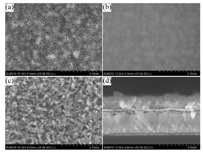
Fig. 1 shows the morphology of BiVO4 and their composites. The top-view SEM image of the pristine BiVO4 film displays the worm-like porous structure (Fig. 1(a)). After coating 286 cycles of ALD ZnO on the BiVO4 film, the pores disappear obviously (Fig. 1(b)). If reducing the ALD-cycles of ZnO, the pores cannot be completely covered, as shown in Fig. S1. Fig. 1(c) and (d) exhibit the top and cross-sectional view of BiVO4/CuO prepared by a cation ion-exchange process in a water bath. The CuO has the uniform petalage-like morphology composed of one-dimensional (1D) nanocones. The 1D nanocones are directly attached to the surface of BiVO4 and have the length of about 350 nm, which is beneficial to the charge transport in a particular direction. Meanwhile, the separated 1D structure facilitates the penetration of electrolyte between nanocones and has increased contact area with electrolyte. It is noted that CuO nanocones cannot be grown on the BiVO4 films without ZnO sacrificial layers (Fig. S2).
Fig. 1. Top-view SEM images of (a) pristine BiVO4, (b) BiVO4/ZnO and (c) BiVO4/CuO substrates, (d) Cross-sectional SEM image of BiVO4/CuO.
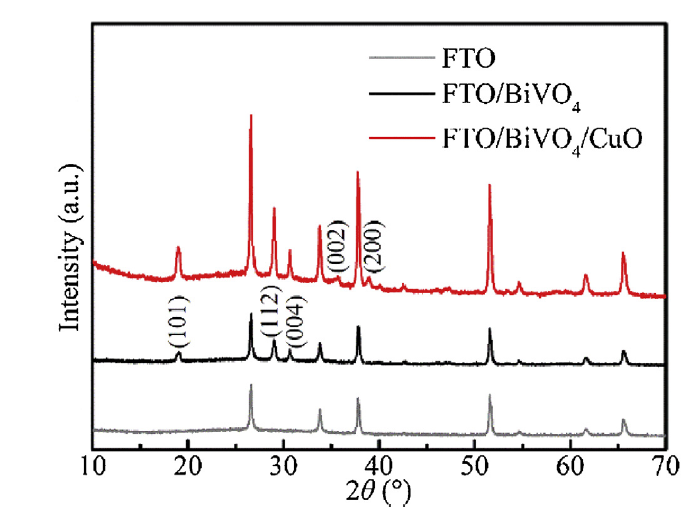
Fig. 2 shows the XRD pattern of BiVO4 and BiVO4/CuO films. Except for the peaks corresponding to the FTO, other diffraction peaks at 2θ = 18.9°, 28.9° and 30.64° are assigned to the (101), (112) and (004) plane of monoclinic BiVO4 (JCPDS 83-1699), respectively. Two weak peaks at 2θ = 35.4° and 38.9° are well indexed to tenorite CuO (JCPDS 48-1548) [23]. There are no obvious peaks corresponding to Zn in the full spectrum of the BiVO4/CuO (Fig. S3), indicating that ZnO is fully changed into CuO and there is no excess ZnO. As for the BiVO4/CuO/TiO2, both the SEM image and XRD pattern do not show clear distinction compared to the BiVO4/CuO (Fig. S4), which is due to the ultrathin thickness of TiO2 as previously reported [24]. There is no detectable peaks after the deposition of TiO2 on CuO surface, but the intensity of all diffraction peaks decreases. This means the thin TiO2 layer is possibly coated onto the surface of CuO. To further verify the existence of TiO2, the EDS elemental mapping was performed. As shown in Fig. S5, Ti elements distribute uniformly on the surface of CuO.
Fig. 2. XRD pattern of FTO, BiVO4 and BiVO4/CuO composite.
XPS was utilized to inspect the surface composition and oxidation state of BiVO4/CuO. The high-resolution XPS spectra of the Bi 4f, V 2p, O 1 s and Cu 2p are shown in Fig. S4. Two characteristic peaks located at 159.4 and 164.7 eV arising from Bi 4f7/2 and Bi 4f5/2 signals suggest Bi ions are present as Bi3+ (Fig. S6(a)). The peaks at 517 and 524.1 eV are assigned to V 2p3/2 and V 2p1/2 (Fig. S6(b)), respectively, confirming the existence of V5+ ions. The O 1 s spectrum is consisted of three peaks at 529.4, 530.9 and 533.3 eV (Fig. S6(c)), representing the lattice oxygen, surface hydroxide, and surface absorbed water, respectively. The Cu 2p spectrum displays two main peaks, one at 933 eV with two satellites at 941.4 and 943.5 eV and the other one at 953.3 eV with a satellite at 961.6 eV (Fig. S6(d)), presenting the Cu2+ oxidation state. These results evidence that the BiVO4/CuO has been successfully fabricated.
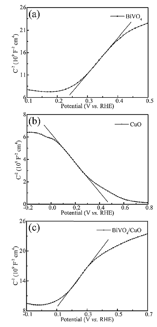
M-S measurements were conducted to investigate their semiconducting feature for pure BiVO4, pure CuO and BiVO4/CuO heterojunctions at 1.0 kHz frequency under dark condition. The positive slope in the M-S plot indicates BiVO4 is a typical n-type semiconductor (Fig. 3(a)), in accordance with pervious report. CuO exhibits the p-type semiconducting behavior as expected, which is confirmed by the negative slope in Fig. 3(b). In Fig. 3(c), the as-fabricated BiVO4/CuO heterojunctions possesses the n-type semiconductor character and thus is suitable as the photoanode of PEC water splitting. The carrier density Nd can be estimated from the slope of the M-S plots by the equation as follows [25]
C-2=($\frac{2}{e_0εε_0N_dA^2}$)[V-VFB-$\frac{κT}{e_0}$] (4)
where C is the specific capacity, ε is the dielectric constant of samples, ε0 is the electric permittivity of vacuum, Nd is the carrier density, A is the area, V is the applied potential, VFB is the flat band potential, κ is the Boltzmann constant, T is the absolute temperature, and e0 is the electron charge. The slope of BiVO4/CuO is smaller than pure BiVO4, indicating higher carrier density. This implies the introduction of CuO not only increases the charge carrier separation ability, but also improves carrier density. Thus, increased photocurrent density can be expected for the heterojunctions.
Fig. 3. Mott-Schottky spectra of (a) BiVO4, (b) CuO and (c) BiVO4/CuO.
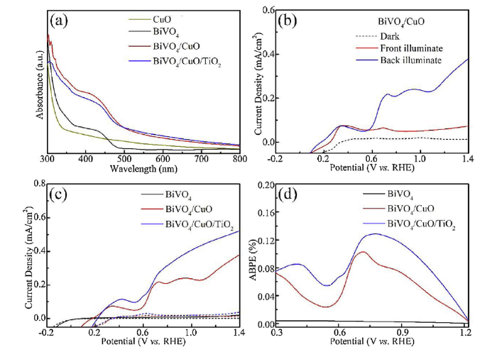
The light harvesting capability was evaluated by measuring the absorption spectra of CuO, BiVO4, BiVO4/CuO, and BiVO4/CuO/TiO2 photoanodes, as shown in Fig. 4(a). The absorption edge of pure BiVO4 and CuO is about 500 and 590 nm, respectively, corresponding to the direct band energy of 2.48 and 2.10 eV. The BiVO4/CuO heterojunction has a higher light absorption in the measured spectral range compared to pure BiVO4 and CuO, because the narrow bandgap of CuO extends the absorbance toward the long-wavelength direction. Meanwhile, the petalage-like morphology of CuO strengthens the light scattering effect. The enhanced light absorption capability is beneficial to the generation of more photo-excited carriers. Depositing TiO2 film on CuO does not change obviously the light absorption. This suggests that the PEC performance enhancement (shown in the following section) upon loading of TiO2 is not due to the increased light utilization.
Fig. 4. (a) Absorption spectra of as-prepared samples, (b) J-V curves of BiVO4/CuO under simulated solar light (front and back illumination) and dark condition, (c) J-V curves of BiVO4, BiVO4/CuO and BiVO4/CuO/TiO2 under back illumination (solid line) and in dark (dashed line) and (d) corresponding ABPE curves.
The photocurrent density of the BiVO4/CuO heterojunction photoanode was measured under both the front- and back-side illumination (Fig. 4(b)). Back-side illumination leads to much higher photocurrent density as compared to that under front-side illumination when the working voltage exceeds 0.6 V vs. RHE. The same phenomenon was also found in the previous reports [26,27]. This is attributed to the fact: when light illuminates the electrode from back side, a large amount of electrons are produced at the interface between BiVO4 and FTO, which is beneficial for electron transfer to counter electrode without passing through the bulk of BiVO4. If front-side illumination is applied, the photogenerated electrons have to travel through BiVO4 film, increasing mass bulk recombination and thus leading to reduced photocurrent. To exclude the influence of illumination direction on the light harvesting capability, the absorption spectra of the samples were measured (Fig. S7). The result reveals that there is no obvious difference for the absorption under the front- or back-side illumination. Therefore, the remarkable performance difference is not caused by the light absorbance capacity. Noted that the following PEC measurements will be performed under back-side illumination. The effect of the thickness of BiVO4 films on PEC performance was explored by adjusting the spin-coating times and speed, as shown in Fig. S6. Increasing the spin-coating times with the same speed at 4000 rpm, the photocurrent first increases and then shows an invariable trend (Fig. S8(a)). The same phenomenon for the spin-coating speed is shown in Fig. S8(b). More times and slower speed give rise to larger thickness, which boosts the light absorption efficiency. However, the thicker thickness will cause serious carrier recombination in bulk, because the photogenerated electrons tend to react with holes in the long travelling distance, but do not transfer to FTO substrate. Thus, the spin-coating times and speed must be controlled well to achieve an optimized performance for BiVO4/CuO photoanode. We also investigated the effect of ZnO sacrificial layer thickness on the PEC performance. Fig. S9(a) shows the J-V curves of BiVO4/CuO reacted from different thickness (ALD cycles) of ZnO at the same reaction time of 45 min. No obvious difference is shown, indicating that the thickness of ZnO sacrificial layer has negligible effect on the growth of CuO nanocones (Fig. S10). When the BiVO4/CuO is obtained from the same thick ZnO with different reaction time from 15 to 45 min, as shown in Fig. S9(b), the photocurrent density increases slightly. The less reaction time leads to poorer performance because the displacement reaction is possibly not accomplished, which can be reflected in the difference of morphology (Fig. S11). The 15 min reaction produces less CuO nanostructure as compared to the 45 min reaction, resulting in fewer reaction sites between photoanode and electrolyte. The BiVO4/CuO junction exhibits largely increased photocurrent density than the pure BiVO4 photoanode under the same measurement condition (Fig. 4(c)). The PEC property is further enhanced after the deposition of a thin layer of TiO2 on the BiVO4/CuO. The photo-conversion efficiencies of BiVO4, BiVO4/CuO and BiVO4/CuO/TiO2 under different bias voltages are calculated (Fig. 4(d)). The huge advance of PEC performance and photo-conversion efficiency for BiVO4/CuO compared to pure BiVO4 arises from three factors: i) the built-in electric field of p-n junction promotes the charge carrier separation and suppresses the carrier recombination in the bulk, ii) 1D CuO increases the contact area between photoanode and electrolyte, providing more reaction sites, and iii) the petalage-like structure enhances the light-harvesting capability and more charge carriers are generated to contribute photocurrent.
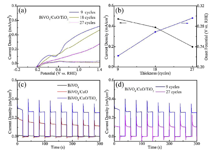
To explore the influence mechanism of TiO2 films on the PEC performance, different thickness amorphous TiO2 was deposited on the BiVO4/CuO. The detailed J-V curves are shown in Fig. 5(a). Fig. 5(b) summarizes values of the current density at 1.23 V vs. RHE and the onset potential (Von) for samples deposited by different thickness (ALD cycles) of TiO2. With increasing the thickness, the photocurrent density declines rapidly and attains the maximum value at the thinnest thickness, and the Von shifts continuously toward the positive potential. It is known that the valence band of TiO2 is more positive than CuO, hindering photogenerated holes in CuO from transferring into electrolyte. If the thickness of TiO2 is very thin, holes can tunnel through the TiO2 to participate in the oxygen evolution reaction. However, the thick TiO2 will seriously block holes transport to electrolyte and cause carrier recombination at the CuO/TiO2 interface. In addition, the thin amorphous TiO2 can passivate the surface defect states of CuO.
Fig. 5. (a) J-V curves of BiVO4/CuO/TiO2 composites with different TiO2 thickness, (b) The current density at 1.23 V vs. RHE and the onset potential as a function of TiO2 thickness, (c) J-t curves of BiVO4, BiVO4/CuO, BiVO4/CuO/TiO2 at 1.23 V vs. RHE, (d) J-t curves of BiVO4/CuO/TiO2 composites (9 and 27 cycles of TiO2 thickness) at 1.23 V vs. RHE.
The J-t curves of BiVO4, BiVO4/CuO, and BiVO4/CuO/TiO2 are shown in Fig. 5(c). The negative current spike of BiVO4/CuO/TiO2 is weaker compared to BiVO4/CuO, suggesting less back electron/hole recombination when light is switched off. This demonstrates TiO2 enhances charge transfer ability and reduces surface recombination. As the thickness of TiO2 increases to 27 cycles (Fig. 5(d)), the negative current transient appears again because the thick TiO2 seriously blocks holes transport to electrolyte. These results further confirm that the ultrathin amorphous TiO2 can eliminate defect states, leading to higher PEC performance.
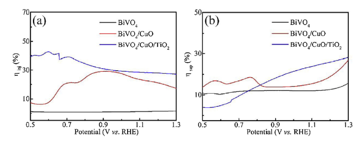
The charge separation efficiency (ηsep) is defined as the fraction of the photogenerated holes reaching the electrode/electrolyte interface, reflecting the recombination rate and separation capability of carriers in bulk. The charge injection efficiency (ηinj) is the fraction of those holes at the photoanode/electrolyte interface used for water oxidation, therefore, it would be enhanced by reducing surface recombination and by increasing oxygen evolution kinetics of holes. To quantify the contribution of CuO and TiO2 to the PEC enhancement, the ηsep and ηinj were acquired by using Na2SO3 as the hole scavenger. Na2SO3 can be used as a hole scavenger to harvest photoexcited holes with nearly 100% efficiency as previous studies. With the assumption that the hole collection efficiency is 100% when Na2SO3 is used as the hole scavenger, it is possible to estimate ηinj by calculating the photocurrent ratio measured without/with Na2SO3. In this way, the ηsep can also be estimated by dividing photocurrent density measured with Na2SO3 by the light absorption efficiency. Fig. 6(a) and (b) show the ηinj and ηsep of as-prepared samples. It is shown that the ηinj of as-prepared BiVO4/CuO is significantly enhanced, reaching to 20.06% at 1.23 V vs. RHE, which is 14 times higher than that of pure BiVO4 (1.43% at 1.23 vs. RHE). Upon depositing TiO2 on BiVO4/CuO, the ηinj further increases to 27.73% at 1.23 vs. RHE. The increased ηinj is because the amorphous TiO2 passivates the surface defect states of CuO and effectively reduces the surface recombination of charge carriers. In addition, BiVO4/CuO sample has a ηsep of 20.94% at 1.23 vs. RHE, in comparison with 13.23% of pristine BiVO4. The remarkable enhancement of ηsep is ascribed to the formation of p-n junctions between CuO and BiVO4, which promotes the photogenerated electron-hole pairs separation and thus greatly reduces the bulk recombination. As TiO2 is deposited on the surface of CuO, the ηsep reduces at the low bias range. This is because the band position of TiO2 does not match with CuO, which goes against charge separation, leading to bulk recombination. While at the higher bias range, the holes are able to tunnel through the ultrathin TiO2 film and realize fast photogenerated electron-hole separation. As the thickness of TiO2 further increases to 27 cycles (Fig. S12), the ηinj become much higher but the ηsep become much lower, which further confirms that thicker amorphous TiO2 films passivate surface defects but hinder the transfer of holes.
Fig. 6. (a) Injection and (b) separation efficiency of BiVO4, BiVO4/CuO and BiVO4/CuO/TiO2.
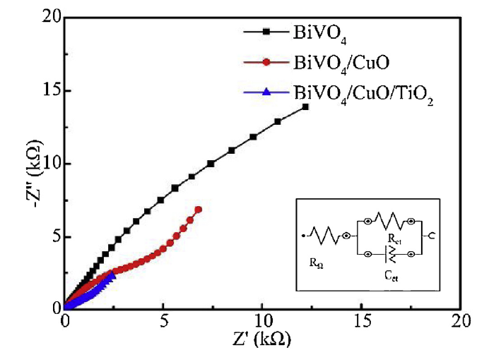
EIS was measured to reveal the electrochemical behavior of photoanodes at the open-circuit voltage in the frequency range of 0.1 Hz to 100 kHz [28,29]. Fig. 7(a) shows the typical Nyquist plots of different photoanodes with the inserted equivalent circuit. The series resistance (RΩ) is equivalent to charge transport, containing the resistance of FTO substrate, semiconductor, and electrolyte, and so on. The reduction reaction at the Pt counter electrode corresponds to the high frequency (more than 1200 Hz), and the middle frequency (below 100 Hz) represents the charge-transfer resistance (Rct) at the photoanode/electrolyte interface. The smaller radius of the circular arc in the middle frequency indicates the smaller charge-transfer resistance. The detailed values for the RΩ and Rct are shown in Table 1. After CuO deposition, the radius declines obviously, and the BiVO4/CuO/TiO2 presents the smallest radius. These EIS results suggest that the BiVO4/CuO p-n junction accelerates the charge transfer, and TiO2 reduces the defects and improves holes capture at the surface of electrodes, accounting for improved PEC performance.
Fig. 7. Nyquist plots of BiVO4, BiVO4/CuO and BiVO4/CuO/TiO2 measured at an open-circuit voltage with the inserted equivalent circuit in the bottom-right corner to fit the EIS data.
Table 1 Fitted series and charge transfer resistances from EIS data.
| RΩ (Ω) | Rct (kΩ) | |
|---|---|---|
| BiVO4 | 48.2 | 43.4 |
| BiVO4/CuO | 48.0 | 10.9 |
| BiVO4/CuO/TiO2 | 47.4 | 0.9 |
In summary, we have designed and synthesized the TiO2 modified p-CuO/n-BiVO4 heterojunctions by spin-coating, water bath reaction, and ALD methods. The synergetic effect of morphology, energy band, and surface passivation in the BiVO4/CuO/TiO2 heterojunction result in largely improved PEC performance, namely a photocurrent of 0.479 mA cm-2 at 1.23 V vs. RHE is achieved. The 1D petalage-like CuO increases the charge transfer between photoanode and electrolyte and the light harvesting ability, the p-n junction improves the charge separation and reduces the bulk recombination, and the surface states passivation decreases the surface recombination and enhances the charge injection efficiency. The present results demonstrate a synergetic surface and interface strategy for constructing efficient heterojunction photoelectrodes of PEC water splitting.
L. Meng and W. Tian contributed equally to this work. This research was supported by the National Natural Science Foundation of China (51772197, 51422206, 51372159), 1000 Youth Talents Plan, Key University Science Research Project of Jiangsu Province (17KJA430013), 333 High-level Talents Cultivation Project of Jiangsu Province, Six Talents Peak Project of Jiangsu Province, and Funded by the Priority Academic Program Development of Jiangsu Higher Education Institutions (PAPD).
The authors have declared that no competing interests exist.

 WeChat
/
| 〈 |
|
〉 |