Search for articles:
C. Guillén , J. Herrero
Corresponding authors:
Received: 2018-11-22
Revised: 2018-12-18
Accepted: 2019-01-26
Online: 2019-08-05
Copyright: 2019 Editorial board of Journal of Materials Science & Technology Copyright reserved, Editorial board of Journal of Materials Science & Technology
More
Abstract
SnO is an ideally suitable p-type conductive material, with large hole mobility, and has attracted great interest in connection with next-generation electronic applications. In the present work, tin oxide (SnOx) thin films were deposited on unheated soda lime glass substrates by reactive DC sputtering from a pure Sn target. The structural, optical and electrical properties of the films were analysed as a function of the oxygen partial pressure in the sputtering atmosphere and of the post-deposition annealing temperature in air. A structural analysis was carried out using Raman spectroscopy and X-ray diffraction. Optical and electrical characterizations were performed using photo-spectrometry and Hall effect measurements, respectively. The films grown at room temperature and low oxygen pressures reached high deposition rates of above 45 nm/min, showing poorly crystalline SnO and low transparency. Subsequent heating to 350 °C allowed to achieve a more crystalline tetragonal SnO with an average visible transmittance of 65%, a p-type conductivity of 0.8 S/cm, and a hole mobility of 3.5 cm2/(V s).
Keywords:
Metal oxide thin films have been extensively developed due to their broad applications in electronics and photonics [1,2]. They often have the additional benefit of optical transparency, due to their wide band gaps [2]. Since oxide semiconductors show commonly n-type conductivity, much research effort is currently being focused on the achievement of p-type counterparts [3]. The performance of p-type oxide materials is mainly limited by the low mobility of holes in the valence band compared to the mobility of electrons in the conduction band. This is due to the intrinsic electronic structure of metal oxides, where the top of the valence band contains strongly localized O 2p-derived orbitals that lead to large effective masses of holes [4]. One approach of improving p-type conductivity is to employ a material, in which the valence band maximum is formed of hybridized orbitals of O 2p and appropriate orbitals of neighbouring metal cations. SnO is therefore a good candidate, because the tin (II) oxidation state involves contributions from Sn 5s states near the top of the valence band, thus reducing the localization of the valence band edge and facilitating the mobility of holes [5,6].
The origin of p-type conductivity of SnO is attributed to Sn vacancies, which form preferentially under oxygen-rich conditions [7]. In this situation, some cations will be transformed into Sn3+ to maintain charge neutrality, equivalent to Sn2+ and a weakly bonded hole [8]. Experimentally, tin monoxide thin films have been obtained with p-type conductivity and a direct gap energy of about 2.9 eV [9], but its range of formation is narrow in comparison with the tin dioxide compound, which shows n-type conduction and a wider band gap above 3.6 eV [10]. Slight variations in the deposition conditions may result in mixed phases of SnO with metallic Sn and/or SnO2 impurities, leading to irregular electrical conduction in the films [11,12]. This is because SnO tends to be oxidized to SnO2 and decomposes into metallic Sn and SnO2 above a certain temperature, either directly or through the formation of intermediate compounds such as Sn2O3 or Sn3O4 [13,14]. Internal disproportion is observed at 270 °C for powder SnO samples annealed in vacuum conditions [15], but the stability of SnO thin films is strongly dependent on the preparation method and the initial oxygen content apart from the annealing temperature [10,16,17].
Reactive sputtering methods have been widely used to deposit tin oxide thin films with different stoichiometries. Several works have aimed to obtain pure SnO or SnO2 layers by changing the sputtering power and pressure [[17], [18], [19]], the O2 content in the working gas [[20], [21], [22], [23]] or by subsequent heating [[24], [25], [26]]. Air annealing is a preferred procedure to achieve Sn-deficient (or oxygen-rich) SnO with p-type conductivity and a good crystallinity that contributes to improvements in the electrical performance. However, the annealing temperature is usually maintained below 300 °C [[26], [27], [28]] in order to avoid overoxidation and/or disproportion towards SnO2 formation. In general, oxygen-rich conditions are needed to obtain SnO thin films with a high hole concentration, although other studies have indicated an enhancement of the hole mobility of SnO grown in a Sn-rich environment [[29], [30], [31]]. It has been shown that pure SnO is not necessarily the highest mobility phase, since well-controlled amounts of residual metallic tin can increase the hole mobility [29,30]. This fact has been ascribed to the formation of Sn interstitials and O vacancy defects that modify the valence band, inducing higher contributions from the delocalized Sn 5p orbitals compared to the localized O 2p orbitals [32].
In the present work, tin oxide thin films were obtained by reactive DC magnetron sputtering from a metallic target, varying the oxygen-to-argon partial pressure ratio over a wide range to include Sn-rich and O-rich extremes. The sputtering conditions were adjusted to obtain high deposition rates above 30 nm/min, which are suitable for large-scale applications, without damage to the metallic target. These growth rates are close to that achieved in the pure metallic mode [24,25] and well above values reported for other tin oxide films, which are typically below 10 nm/min [[19], [20], [21], [22],29]. The structural, optical and electrical properties are investigated for the as-grown layers on unheated glass substrates and after annealing in air at various temperatures from 200 °C to 450 °C, with main objective of determining the best deposition and/or heating parameters to maximize the visible transmittance and p-type conductivity of the coatings. The obtained results can provide a significant addition to the knowledge base for the fabrication and the physical properties of tin oxide films.
Tin oxide layers were prepared on unheated soda-lime glass substrates by reactive DC magnetron sputtering from a Sn disc (purity 99.99%) of diameter 15 cm. After evacuation of the chamber to a base pressure of 4 × 10⁻⁴ Pa, oxygen and argon gases were introduced by independent mass flow controllers. The argon flow was maintained at a constant 60 SCCM, resulting in a change in the pressure to 0.4 Pa, while the oxygen flow was varied to achieve different oxygen partial pressures (Opp) of between 6% and 27%, stated as a percentage of the total gas pressure. Then, a DC power of 200 W was applied to the target and the deposition time was adjusted to obtain a film thickness of 0.2 μm, a value that is commonly used [11,[21], [22], [23], [24]]. Post-deposition annealing of the samples was performed in air at temperatures ranging from 200 °C to 450 °C for 30 min.
The thickness of each layer was measured with a Dektak 3030 profilometer. This value and the corresponding deposition time were used to calculate the growth rate (r = thickness/time) for the various oxygen ratios. The microstructure of the samples was analysed with a B&W Tek system consisting of a BAC151B microscope and an i-Raman spectrometer, using a green laser of wavelength 532 nm as the excitation source. The crystallographic properties were examined by X-ray diffraction (XRD) with radiation Cu Kα1 (λ = 1.54056 Å) using a Philips X'pert instrument with a Bragg-Brentano θ-2θ configuration. Crystalline phases were identified by comparison with the cards issued by the Joint Committee of Powder Diffraction Standards. The mean crystallite size was estimated using the Scherrer formula based on the full width at half maximum of the main diffraction peak. The optical characterization used transmittance (T) and reflectance (R) measurements that were made with a double beam spectrophotometer Perkin-Elmer Lambda 9 at wavelengths from 300 to 1500 nm, taking the air as reference. In order to eliminate the interference peaks, the transmittance was corrected for reflection losses using the formula [33]: Tc(%) = 100 T(%)/(100 - R(%)). Electrical conductivity, free charge carrier concentration and mobility were determined with an ECOPIA system based on Hall effect measurements.
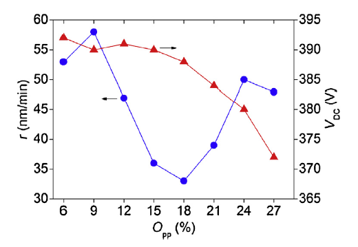
The effect of the oxygen partial pressure on the growth rate of the films is illustrated in Fig. 1, which includes also the corresponding target self-bias. This is observed to be practically constant (390 ± 2 V) in the range of 6% to 18% Opp and then to decrease at higher oxygen ratios. This voltage decrease is typical of the transition region from metallic to reactive sputtering mode [34]. Within the metallic mode, high deposition rates of above 45 nm/min are reached for Opp ≤ 12% (Fig. 1). The reduction in the film growth as the oxygen ratio increases, attaining a minimum of 33 nm/min at 18% Opp, is related to the progressive oxidation of the target surface, since the sputtering rate is in general lower for oxides than for pure metal [22,24,25]. Nevertheless, the growth velocity is found to increase for oxygen proportions above 18%, where the self-bias decrease indicates a further oxidation of the target surface. The alteration in the trend is attributed to a gradual change in the oxidation state of the surface from Sn2+ to Sn4+ when the oxygen ratio increases from 18% to 24% Opp. This is according to other works that have stated that tin has a valence +4 only for cathode voltages below a certain value around 380 V [35,36]. Such a small voltage is here achieved for Opp ≥ 24%; but at lower oxygen proportions, or higher target voltages, a mixture of Sn2+ and Sn4+ states can be expected [36].
Fig. 1. Evolution of the film growth rate and the target self-bias as a function of the oxygen partial pressure in the sputtering atmosphere.
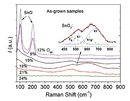
These tin oxide films grown on unheated substrates have poor crystallinity, since no peaks for the oxide compounds appear in the X-ray diffractograms. Small peaks corresponding to metallic Sn are observed for the layers prepared at Opp ≤ 9%, the only samples with an opaque appearance. More information about the microstructure of the as-deposited films has been obtained from the Raman spectra displayed in Fig. 2. For low oxygen proportions, Opp ≤ 12%, the Raman spectra reveal two peaks centred at 105 ± 2 cm-1 and 204 ± 2 cm-1. These correspond to the characteristic B1g (115 cm-1) and A1g (211 cm-1) vibrational modes of bulk tetragonal SnO [8,21,24,37], taking into account the fact that shifts to lower wave numbers are expected for crystallite sizes of below 20 nm [38]. When the oxygen ratio increases to 15%-21% Opp, the Raman intensity remains high in the 75-200 cm-1 region, although SnO peaks are not clearly evidenced. Some increase in the Raman intensity is also observed between 400 and 800 cm-1, which can be attributed to the formation of SnO2. This is because for SnO2 with poor crystallinity, the classical vibration modes A1g (638 cm-1) B2g (782 cm-1) and Eg (476 cm-1) can be together with three wide bands S1 (centred around 570 cm-1), S2 ($\widetilde{5}$00 cm-1) and S3 ($\widetilde{7}$00 cm-1) that appear as a consequence of disorder activation [39,40]. The deconvolution of the experimental spectrum that is obtained for 18% Opp (Fig. 2) shows a predominance of the S1 and S3 bands. However, no evidence of SnO or SnO2 is found for the layers prepared at the greatest oxygen ratios (Opp ≥ 24%), and this fact suggests that the microstructural order decreases for such high oxygen proportions.
Fig. 2. Raman spectra for tin oxide films grown at different oxygen partial pressures.
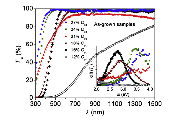
The evolution of the optical characteristics of the layers as a function of the oxygen partial pressure is illustrated in Fig. 3. This shows that a high visible transmittance of above 80% is obtained for the films prepared at Opp ≥ 15%, with a significant displacement of the absorption edge towards lower wavelengths (higher radiation energies) when the oxygen content increases. The band-gap energy (Eg) estimated by the inflection-point method [41] is the maximum of the differential of Tc, as represented in the inset to Fig. 3. The samples prepared with 15%-18% Opp give a value of Eg = 2.8 ± 0.1 eV, which is typical of SnO [9,23]. For lower oxygen ratios (Opp ≤ 12%), a significant decrease in the transparency across the spectrum is observed and is attributed to the coexistence of some metallic Sn°, which reduces the overall optical gap to below 2.0 eV [9]. Otherwise, the layers deposited at 24%-27% Opp show characteristics of SnO2 (Eg ≥ 3.5 eV) [10,22], whereas a mixture of SnO and SnO2 features is observed in the intermediate range of 18% < Opp < 24%. In particular, the layer prepared at 21% Opp has a unique transmittance shape that indicates the formation of regular SnO2 together with SnO islands, which reduce the visible transparency without the typical cutoff that is observed for uniform SnO at λ $\widetilde{4}$50 nm.
Fig. 3. Optical transmittance data obtained for tin oxide films grown at different oxygen partial pressures.
In order to better compare the various samples, the average visible transmittance (within the range λ = 400-800 nm) and the electrical conductivity are represented together in Fig. 4. For these as-grown layers, p-type conductivity was obtained when the oxygen proportion was maintained in the region Opp = 12%-18%. Although SnO formation at lower oxygen ratios was detected by Raman spectroscopy (Fig. 2), the presence of some metallic Sn acts to decrease the optical transmittance [9,21] and confers n-type conductivity to the samples prepared at Opp ≤ 9%. The best combination of transparency and p-type conductivity is attained here at 15% Opp, which is thought to correspond to oxygen-rich SnO material, with acceptor Sn vacancies being responsible for a net hole concentration of N = +1.7 × 1013 cm-3 with a high mobility of μ = 7.8 cm2/(V s) (as shown in Table 1). The decrease in the p-type conductivity at 18% Opp is attributed to the formation of a certain amount of SnO2, as was identified in the corresponding Raman spectra of Fig. 2, but in a discontinuous shape that means the optical and electrical characteristics of the SnO phase are prevalent. Both SnO and SnO2 features are observed for 21% Opp, where the change to n-type conductivity indicates the formation of continuous SnO2; this gives oxygen vacancy donors with an overall carrier concentration of N = -3.5 × 1019 cm-3, and coexists with SnO islands that reduce the optical transmittance. For higher oxygen ratios (Opp ≥ 24%), the optical and electrical characteristics are typical of SnO2 with a wide band-gap energy of above 3.5 eV and n-type conductivity that decreases as the oxygen content increases, because the proportion of donor oxygen vacancies decreases [22]. It should be noted that the conductivity is mainly controlled by the carrier concentration, which changes by several orders of magnitude with small variations in the oxygen content [21]. Conversely, the mobility is almost constant at around 7 ± 1 cm2/(V s) for 1012 < N < 1018 cm-3, but this decreases sharply for higher N values, as observed for other tin oxide layers when the carrier concentration increases [21,30].
Fig. 4. Evolution of the average visible transmittance, electrical conductivity and carrier mobility for the as-grown tin oxide layers as a function of the oxygen partial pressure.
Table 1 Optical properties (visible transmittance) and electrical characteristics (carrier density, mobility and conductivity) obtained for films grown at different oxygen ratios.
| Opp (%) | Tvis (%) | N (cm-3) | μ (cm2/(V s)) | σ (S/cm) |
|---|---|---|---|---|
| 6 | 0.3 | +2.3 × 10²⁰ | 0.2 | 7.3 |
| 9 | 0.4 | +6.5 × 10¹⁹ | 0.1 | 1.0 |
| 12 | 11.6 | +5.0 × 10¹⁵ | 7.4 | 6.0 × 10⁻³ |
| 15 | 82.7 | +1.7 × 10¹³ | 7.8 | 2.1 × 10⁻⁵ |
| 18 | 82.8 | +1.9 × 10¹² | 6.8 | 1.9 × 10⁻⁶ |
| 21 | 82.7 | -3.5 × 10¹⁹ | 0.8 | 4.7 |
| 24 | 97.4 | -5.1 × 10¹⁷ | 6.0 | 4.9 × 10⁻¹ |
| 27 | 97.6 | -1.7 × 10¹⁶ | 6.7 | 1.8 × 10⁻² |
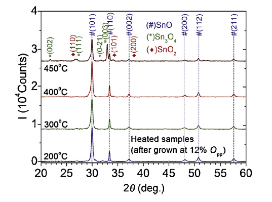
For the tin oxide films prepared in the interval 12%-18% Opp, which have p-type conductivity but poor crystallinity in the as-grown conditions, subsequent annealing in air produces a material crystallization that depends greatly on the oxygen ratio as well as the annealing temperature. The XRD diagrams in Fig. 5 show that the layers deposited at 12% Opp have crystallized in the romarchite SnO phase after heating at T ≥ 200 °C, since they exhibit diffraction peaks from the (101), (110), (002), (200), (112) and (211) planes according to the standard tetragonal structure (JCPDS card No 06-0395), with no evidence of any other crystalline phase. The mean crystallite size increased from 24 to 28 nm when the temperature was raised from 200 °C to 400 °C. Larger crystallites of SnO of about 30 nm were obtained by increasing the heating temperature to 450 °C; but with additional phases that were identified as tetragonal SnO2 (JCPDS card No 41-1445) and triclinic Sn3O4 (JCPDS card No 20-1293), which show crystallite sizes of 20 and 35 nm, respectively. Sn3O4 is an intermediate oxide (with tin in both Sn2+ and Sn4+ states) that is typically formed during the oxidation from SnO to the most stable SnO2 phase [14,42,43]. In the present samples, the SnO phase remains unchanged up to 400 °C in air (Fig. 5), showing better stability than powdered SnO [15]. Thus, an oxygen-poor preparation atmosphere is proven to be useful in improving the thermal stability of SnO thin films [10,17].
Fig. 5. XRD diagrams corresponding to tin oxide films prepared at 12% Opp and subsequently heated in air to different temperatures.
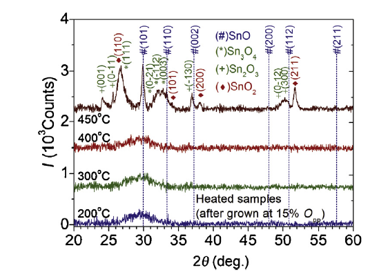
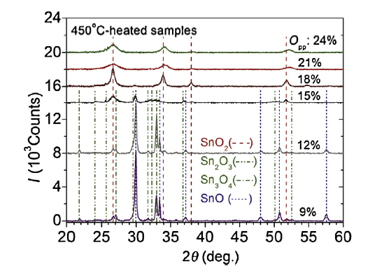
Sn2O3 (JCPDS card No 25-1259) is another intermediate oxide that appears together with Sn3O4, SnO and SnO2 in the diffractogram of Fig. 6 corresponding to the film grown at 15% Opp and heated to 450 °C. This sample exhibits a mean crystallite size of 20 nm for the SnO and a higher proportion of SnO2 crystallites with a minor size of 8 nm. Moreover, only SnO2 with similar sizes (8 ± 2 nm) was identified in the layers prepared at Opp ≥ 18% and annealed at 450 °C, as shown in Fig. 7. At lower heating temperatures, the samples remain amorphous when they are deposited at Opp ≥ 15%. Hence, it is suggested that the presence of some Sn4+ in the SnO matrix boosts the structural disorder and increases the crystallization temperature [21]. On the other hand, Fig. 7 shows that tin oxide films prepared at the lowest oxygen ratios (Opp ≤ 12%) contain large SnO crystallites.
Fig. 6. XRD diagrams corresponding to tin oxide films prepared at 15% Opp and subsequently heated in air to different temperatures.
Fig. 7. XRD diagrams corresponding to tin oxide films prepared at various oxygen ratios and heated in air to 450 °C.
The Raman spectra also evidence SnO crystallization for the films grown at 6%-12% Opp, after heating in air at 200 °C or above, as illustrated in Fig. 8. SnO2 signals appear in these samples when the annealing temperature increases to 400 °C, and are identified as the A1g and B1g fundamental vibration modes together with the bands (S1-S3) that are activated by disorder in the tin dioxide [39,40]. A further increase in the annealing temperature to 450 °C produces additional peaks at low wave numbers, which are attributed to Sn3O4 (with Raman-active modes at 90, 140, 170 and 240 cm-1 [43,44]) and Sn2O3 (with vibrational frequencies at 76, 122, 235 and 300 cm-1 [44]). Here, the formation of SnO2 is observed before that of the intermediate oxides Sn3O4 and Sn2O3. These have triclinic structures that are theoretically formed when some layers of oxygen are removed from the (101) planes of rutile SnO2 [14]. They consist of SnO2-like local structures, in which Sn is quadrivalent, together with SnO-like structures in which it is divalent [45]. In the present samples, both intermediate oxides were detected for Opp ≤ 18%, after heating at 450 °C and in conjunction with SnO2. At higher oxygen ratios, only SnO2 appears in the Raman spectra of the heated films, without significant changes with respect to the corresponding as-grown layers depicted in Fig. 2.
Fig. 8. Raman spectra for tin oxide layers prepared at 12% Opp and heated in air to different temperatures.
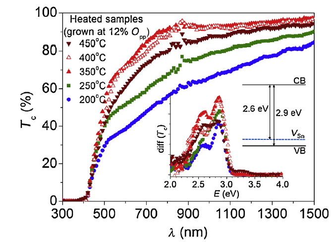
For the samples prepared at Opp ≤ 12%, a significant improvement in the optical transmittance is obtained by increasing the annealing temperature from 200 to 400 °C, as illustrated in Fig. 9. However, a worsening occurs at 450 °C, which is related to the crystallization of SnO2 and intermediate oxides in competition with the main SnO, as evidenced by the corresponding XRD and Raman spectra in Fig. 5, Fig. 8. The presence of some metallic Sn is expected after heating to the highest temperature, coming from the disproportionation reaction (2SnO → SnO2 + Sn) [46], which reduces the transmittance values across the whole range of wavelengths [9]. The differential of the transmittance spectra in Fig. 9 shows two marked absorption edges around 2.6 and 2.9 eV. These correspond to the electronic structure of p-type conductive SnO, with an interband transition energy of Eg = 2.9 eV and an acceptor level located at 0.3 eV above the valence band maximum, which is attributed to Sn vacancies [47]. The transition from this acceptor level to the conduction band minimum is clearly distinguished in the layers formed of well-crystallized SnO, since the absorption edges become sharper when the crystallite size increases; however, only the band-to-band transition is evident for the films prepared at higher oxygen ratios, which remain poorly crystalline after heating.
Fig. 9. Optical transmittance data obtained for tin oxide films grown at 12% Opp and subsequently heated in air to different temperatures.
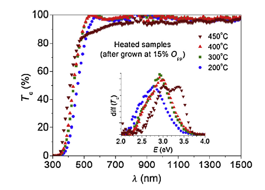
The optical properties of the layers deposited at Opp ≥ 15% show minor variations with the annealing. These are represented in Fig. 10, where a slight displacement of the absorption edge can be seen towards lower wavelengths as the heating temperature increases. For the films prepared at 15% Opp, the optical gap increases from 2.8 to 3.0 eV when the temperature rises from 200 °C to 450 °C. An additional absorption at around 3.4 eV is also observed for the sample heated to the highest temperature. This is attributed to the interband transition of the SnO2 phase, which crystallizes together with SnO and is observed to be predominant in the corresponding diffractogram of Fig. 6. For these layers prepared at 15% Opp, the conductivity changes to n-type when heated to 450 °C, and even at a lower annealing temperature of 350 °C when the films were deposited at 18% Opp, as observed in other works [10,23]. For higher oxygen ratios (Opp ≥ 21%), n-type conductivity is measured in the as-grown and heated samples. Otherwise, p-type conductivity is obtained after annealing the layers prepared at Opp ≤ 12%, with hole density increasing up to 350 °C and then remaining practically unchanged at higher temperatures.
Fig. 10. Optical transmittance data obtained for tin oxide films grown at 15% Opp and subsequently heated in air to different temperatures.
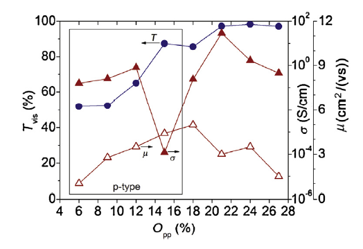
Fig. 11 illustrates the evolution of the optical and electrical characteristics as a function of Opp, for the same samples as in Fig. 4 but after heating to 350 °C. The most transparent p-type layers are those prepared at 15% Opp, with a visible transmittance that increases from 83% to 87% due to the annealing; while the conductivity changes from 2.1 × 10⁻⁵ to 1.2 × 10⁻⁴ S/cm, even when no significant SnO crystallization is achieved in these films. Post-deposition heating is found to be more effective in improving the structural and electrical properties of the samples grown at Opp ≤ 12%, giving well-crystallized SnO with p-type conductivities of above 0.2 S/cm. The best optical and electrical performance is achieved for layers deposited at 12% Opp after annealing at 350 °C, which gives Tvis = 65%, σ = 0.8 S/cm and μ = 3.5 cm2/(V s), optimal data in comparison with those reported for analogous SnO films [23,26,[28], [29], [30]]. Tin oxide layers prepared at Opp < 12% showed similar structural and electrical characteristics after heating, but with lower transmittance. Otherwise, for the highest oxygen ratios (Opp ≥ 21%), n-type conductivities above 0.8 S/cm are obtained with poorly crystalline SnO2. The high conductivity of amorphous SnO2 films has been attributed to the specific electronic configuration of the material [10,48]. The conduction band of SnO2 is formed from spherical Sn 5s orbitals, which maintain the overlap between different atoms in disordered amorphous structures [48]. For p-type SnO, anisotropic O 2p orbits contribute to the valence band formation together with Sn 5s states, and the crystalline order therefore greatly influences the conductivity [10].
Fig. 11. Evolution of the average visible transmittance, electrical conductivity and carrier mobility for tin oxide layers prepared at different oxygen partial pressures and heated in air to 350 °C.
Tin oxide (SnOx) thin films were prepared by reactive sputtering from a pure Sn target, and the tin oxidation state was varied using the oxygen partial pressure during growth on unheated substrates and by posterior annealing in air. The as-grown samples have poor crystallinity, but a good combination of transparency and p-type behaviour is attained at 15% Opp, giving an average visible transmittance of 83% and a conductivity of 2.1 × 10⁻⁵ S/cm. For these layers, the crystallization of SnO is observed with SnO2 and intermediate oxides (Sn3O4 and Sn2O3) only after heating to 450 °C, when the conductivity changes to n-type. At lower annealing temperatures, the samples remain amorphous and p-type, with a maximum visible transmittance of 87% and a hole conductivity of 1.2 × 10⁻⁴ S/cm, which are reached at 350 °C.
The presence of some Sn4+ in the lattice inhibits the SnO crystallization, but this is easily achieved in coexistence with Sn°. Vibrational modes corresponding to tetragonal SnO are clearly detected by Raman spectroscopy in the as-grown layers at high deposition rates (above 45 nm/min) and low oxygen ratios (Opp ≤ 12%), and the mean crystallite size increases as the heating temperature raises. After annealing at 350 °C, the visible transmittance and p-type conductivity of the films grown at 12% Opp increase to 65% and 0.8 S/cm, respectively. Additional phases of SnO2 and intermediate oxides also crystallize around 450 °C, worsening the optical and electrical performance.
This work was financially supported by the Spanish Ministry of Science, Innovation and Universities (No. MAT2015-66649-R).
The authors have declared that no competing interests exist.

 WeChat
/
| 〈 |
|
〉 |