Search for articles:
Changwei Tang
Corresponding authors:
Received: 2018-10-27
Revised: 2018-12-11
Accepted: 2019-01-15
Online: 2019-08-05
Copyright: 2019 Editorial board of Journal of Materials Science & Technology Copyright reserved, Editorial board of Journal of Materials Science & Technology
More
Abstract
Cuprous oxide (Cu2O) is an attractive material for photoelectrochemical (PEC) hydrogen production or photovoltaic application, because of its appropriate band gap, low material cost and non-toxic. In this paper, Cu2O films were obtained by comproportionation in acid cupric sulfate solutions with varying concentrations of potassium nitrate. Photoelectrochemical and electrochemical experiments, such as zero-bias photocurrent responses, voltammograms, and Mott-Schottky measurements, show that the Cu2O films grown in low (≤0.75 mol dm-3) and high (≥1.00 mol dm-3) nitrate ion concentrations presented n-type and p-type conductivity, respectively. Open circuit potential and polarization behavior were monitored to investigate the mechanism of modulating conductivity type. Nitrate ions consume protons in the plating solution during comproportionation with different concentrations of nitrate ions creating different pH at the Cu2O/solution interface. This gradient leads to the transformation of Cu2O films conductivity changing from n-type to p-type with increasing the concentration of nitrate ions in the plating solution. This method could be used to fabricate homojunction electrode on metal substrate for PEC hydrogen production or photoelectric application.
Keywords:
Cuprous oxide (Cu2O) is suitable for electronic applications, such as the hydrogen evolution reaction [1], CO2 reduction [2] and photocatalysis [3]. It has the desired properties of an appropriate band gap (around 2 eV [4]), abundant raw materials and is non-toxic. Various techniques, such as thermal oxidation [5], electrochemical reduction [6], electrochemical anodization [7], magnetron sputtering [8] and chemical oxidation [9,10], have previously been employed to prepare Cu2O films. Many efforts have been made to control the n-type or p-type conductivity of Cu2O films. For instance, through thermal annealing treatment in air or oxygen atmosphere, the conductivity type of Cu2O film is transformed from n-type to p-type due to the introduction of atomic oxygen into Cu2O lattices at high temperature [5]. Electrochemical deposition is a common and convenient method to tune the conductivity type of Cu2O film by properly controlling electrodeposition parameters, such as pH [6,11], surfactant concentration in plating solution [12], and deposition potential [13]. Formation of O vacancies or Cu vacancies in Cu2O film tunes the film to yield n-type or p-type conductivity. Electrochemical methods of producing Cu2O films achieve this by adjusting the reduction rate of cupric ions (Cu2+) to cuprous ions (Cu+) and the concentration of hydroxide ions at the electrode interface. The chemical oxidation method is energy-saving and low-cost, which is advantageous for large-scale production of Cu2O film over thermal oxidation and electrochemical deposition. However, it is challenging to directly oxidize a Cu substrate to pure Cu2O [9]. Undesired Cu(OH)2 film is first formed on Cu substrate when strong oxidizer (e.g., peroxydisulfate) is contained in basic solution. Cu2O film can be obtained by annealing the Cu(OH)2 film afterwards [9,10], however, a mixture of Cu2O and CuO may be formed if the annealing temperature is not appropriate. Among the chemical oxidation methods, the comproportionation through Cu2+ oxidizing Cu substrate to obtain Cu2O film is attractive due to a one-step mechanism and facile synthesis. Cu2+ is the oxidation agent in comproportionation, and thus the valence of copper will not go beyond Cu+. Jin et al. prepared p-type Cu2O film by immersing a copper mesh in concentrated NaOH (2.4 mol dm-3) solution containing 6 × 10⁻³ mol dm-3 copper acetate [11]. Fernando et al. reported that n-type Cu2O layers could be obtained by immersing a copper plate in a CuSO4 (10-3 mol dm-3) solution containing HCl (10-3 mol dm-3) [14], or just boiling copper plates in CuSO4 solution [15]. Employing comproportionation to grow Cu2O films on copper substrates has other advantages such as increased electrical contact between films and substrates, because Cu is not only a substrate but a reactant [11,[14], [15], [16], [17]]. Hence it would benefit the electrical performance for the photoelectrochemical (PEC) or photoelectric devices due to the compact contact at Cu2O/Cu interface.
There are however only a few reports on the fabrication Cu2O film by comproportionation [11,14,15] and no attempt on the conductivity modulation of Cu2O film. For photoelectric or PEC application, homojunction devices are generally expected to have better performance than heterojunction devices due to lattice matching [18]. Thus, controlling p-type or n-type conductivity of Cu2O films by comproportionation is highly attractive. Furthermore, fundamental understanding about conductivity modulation of Cu2O films by comproportionation is essential to guide both lab research and industrial production.
In this paper, Cu2O films were synthesized via a comproportionation between cupric ions and copper foils in a dilute acid plating solution (pH = 5.00). Varying concentrations of potassium nitrate were added into the plating solution to modulate the conductivity type of the Cu2O films from n- to p-type. The growth of Cu2O films by comproportionation and the modulation mechanism of conductivity type of Cu2O films by nitrate ions were discussed in detail.
Copper foil (thickness: 0.1 mm), copper (II) sulfate pentahydrate (CuSO4·5H2O), potassium nitrate (KNO3), sodium chloride (NaCl), sodium DL-lactate (C3H5O3Na) and sodium hydroxide (NaOH) were purchased from Sinopharm Chemical Reagent Co. Ltd. Hydrochloric acid (HCl) and acetone (CH3COCH3) were purchased from Tianjin Fuchen Chemical Reagents Factory. Deionized water (DI water) was produced by Merck Millipore Elixv Advantage Water Purification System.
In a typical procedure, a Cu foil was firstly cut into rectangles (35 mm × 40 mm). Prior to performing comproportionation, all Cu foils were cleaned ultrasonically in dilute HCl (0.5 mol dm-3), acetone and DI water sequentially for 5 min for each wash. The Cu foils were dried and immersed into the plating solutions for 6 h at 30.0 ± 0.2 °C to grow Cu2O films. After finishing the comproportionation, the Cu foils with Cu2O film were taken out and rinsed with DI water.
The plating solution contained CuSO4 (0.1 mol dm-3), C3H5O3Na (0.15 mol dm-3) and varying concentrations of KNO3. The plating solution was adjusted with NaOH solution (3 mol dm-3) to pH 5.00 (The pH of bulk plating solution is stable during 6 h comproportionation, as show in Table S1 in Supporting Information). Lactate ions, used as complexing agents, coordinate with Cu2+ ions, so that the plating solution was buffered to the pKa of lactate at 3.86. The KNO3 concentration was chosen from 0 to 2.00 mol dm-3 (the solubility of KNO3 is about 2.2 mol dm-3 KNO3 in this plating solution) for growing Cu2O films with different conductivity type in the plating solution.
X-ray diffraction (XRD) patterns of Cu2O films were recorded on a D8 Advance X-ray diffractometer (Bruker, Germany) using Cu Kα radiation (λ = 0.15418 nm). Morphologies and thicknesses of Cu2O films were measured by scanning electron microscopy (SEM, SU-8010, Hitachi, Japan) at an acceleration voltage of 5.0 kV. Cross-section components of Cu2O films were analyzed using energy dispersive X-ray spectroscopy (EDS). Surface composition and chemical state of Cu2O films were tested by using an Axis Ultra X-ray photoelectron spectroscope (XPS, Kratos Analytical, UK). The binding energies were corrected by a reference C 1s peak at 284.8 eV. Ultraviolet-visible diffuse reflectance spectra (UV-vis-DRS) were obtained from a U-3310 spectrometer (Hitachi, Japan).
Conductivity types of Cu2O films were characterized through zero-bias photocurrents [12,13], voltammograms under illuminance and dark, and Mott-Schottky measurements [19] in 3 wt% NaCl solution. These measurements were carried out by using a Model 5210 lock-in amplifier (Princeton Applied Research, USA) combined with a 283 potentiostat (Princeton Applied Research, USA). A standard 3-electrode setup was used for PEC characterization. Copper foils with Cu2O films were served as the working electrode, Ag/AgCl (saturated KCl) electrode and Pt foil as the reference electrode and counter electrode, respectively. A CHF-XM-500 W xenon lamp (Beijing Changtuo, China) was adopted as light source (light intensity: 100 mW cm-2) to measure zero-bias photocurrents and photo-voltammograms. Potential ranges of Mott-Schottky measurements were from -0.1 to -0.7 V for n-type Cu2O films and 0 to -0.5 V for p-type Cu2O films, respectively.
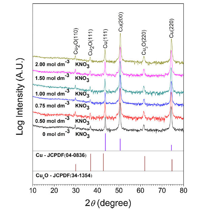
Fig. 1 shows XRD patterns of Cu2O films prepared in plating solutions (pH 5.00) containing different concentrations of KNO3. Three crystal planes (111), (200) and (220) located at diffraction angle (2θ) of 43.30°, 50.43° and 74.13° were indexed to the Cu crystal (JCPDF No. 04-0836), respectively. Three diffraction peaks with weak intensity at 29.98°, 37.01° and 62.44° were corresponded to Cu2O crystal planes of (110), (111) and (220) (JCPDF 34-1354), respectively. No featured peaks of CuO and Cu(OH)2 appeared, implying that Cu2O films growing on Cu foils are pure phase. The (200) diffraction peak of Cu2O was not observed, which could be attributed to the preferential orientation growth covering (200) crystal face of Cu2O film [20]. Furthermore, intensities of each diffraction peak of as-prepared Cu2O films growing with different KNO3 concentrations in the plating solutions were identical, suggesting that NO3- ions had no specific adsorption on Cu2O crystal planes.
Fig. 1. XRD patterns of Cu2O films grown on Cu foils by comproportionation in plating solutions with varying concentrations of KNO3.
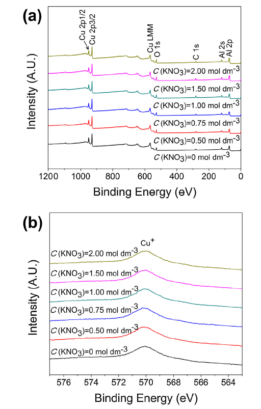
The chemical components of Cu2O films were studied by XPS analyses (Fig. 2). From survey spectra (Fig. 2(a)), no N 1s peak (about 398 eV [21]) appeared, suggesting that no nitrogen was doped in Cu2O films. This result can also be confirmed by EDS analyses on cross-section of Cu2O films (Fig. S1 in Supporting Information). In the high-resolution Cu 2p spectra (Fig. S2 in Supporting Information), distinct peaks at binding energies of 932.4 eV and 952.2 eV could be assigned to Cu 2p3/2 and Cu 2p1/2 spin-orbital electrons [22], respectively. All Cu 2p3/2 peaks showed relatively narrow full width at half maxima (FWHM, 1.3 eV), suggesting pure phase formed. Cu and Cu2O could not be identified by Cu 2p3/2 peaks because of their closer binding energies (about 0.1 eV apart). The chemical state of Cu° and Cu+ can be distinguished from the position of Cu LMM (L-inner level-M-inner level-M-inner level) Auger transition in XPS spectra, which are 568.0 eV and 570.0 eV for Cu and Cu2O [23], respectively. A single peak at 570.1 eV is shown in the Cu LMM Auger spectra for all as-prepared Cu2O films (Fig. 2(b)), only Cu2O was tested and no Cu substrates exposed (the measured location was chosen randomly). The peak intensity and FWHM for Cu 2p spectra are basically same for all Cu2O films synthesized in the plating solutions with different concentrations of KNO3. The result suggested that KNO3 concentration had very small influence on the chemical composition of the films.
Fig. 2. XPS survey spectra (a) and Cu LMM Auger spectra (b) of Cu2O films grown on Cu foils by comproportionation in the plating solutions with varying concentrations of KNO3.
SEM and UV-vis-DRS characterizations on all Cu2O films are shown in Figs.S3-S5 in Supporting Information. The SEM results indicated that Cu2O films growing on Cu foils were dense layers. The absorption edges and band gap energies of Cu2O films grown in the plating solutions with different concentrations of KNO3 were identical. These characterizations indicate that the effect of KNO3 concentration in the plating solution on the surface morphology, phase structure, chemical composition and optical performance of Cu2O films is indistinctive.
In this work, the main defects, Cu vacancies and O vacancies, in the film provide the conductivity [24]. Cu vacancies are negatively charged and attract positive holes to maintain electrical neutrality, however, the attraction between Cu vacancies and holes is weak. Cu vacancies absorbing high enough light energy tend to lose trapped holes, which act as carriers for p-type Cu2O [25,26]. Similarly, the positive O vacancies attract electrons to maintain electrical neutrality. O vacancies absorbing high enough light energy tend to lose trapped electrons, which act as carriers for n-type Cu2O. Therefore, Mott-Schottky technology was employed to characterize Cu vacancy or O vacancy densities in bulk Cu2O films [12].
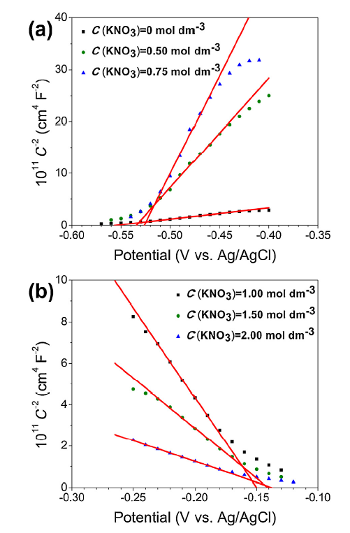
Mott-Schottky curves were measured for all Cu2O films in 3 wt% NaCl solutions for obtaining the semiconducting information (Fig. 3). The Cu2O films showed n-type conductivity when KNO3 concentration was lower than 0.75 mol dm-3 indicated by positive slopes of linear sections in the Mott-Schottky plots (Fig. 3(a)). However, Cu2O films showed p-type conductivity when KNO3 concentration was higher than 1.00 mol dm-3 demonstrated by negative slopes of linear sections in the Mott-Schottky plots (Fig. 3(b)). In addition, the carrier densities and flat band potentials of Cu2O films in 3 wt% NaCl solutions could also be obtained from Mott-Schottky plots and the results are shown in Table 1. The results showed that the carrier densities of n-type Cu2O films gradually decreased, while that of p-type Cu2O films gradually increased with the increase of KNO3 concentration in plating solution. The flat band potentials of Cu2O films moved to more positive potential with the increase of KNO3 concentration. These results indicated that Fermi levels of Cu2O films decreased as KNO3 concentration increased.
Fig. 3. Mott-Schottky plots of Cu2O films grown by comproportionation in the plating solutions with varying concentrations of KNO3.
Table 1 Summary of conductivity types, onset potentials, flat band potentials and carrier densities of Cu2O films obtained through different fabrication methods.
| Electrode | Fabrication Method | Conductivity type | Electrolyte | Onset Potential (V vs Ag/AgCl) (saturated KCl) | Flat band potential (V vs Ag/AgCl) (saturated KCl) | Carrier density (cm-3) | Ref. |
|---|---|---|---|---|---|---|---|
| Cu/Cu2O | Chemical oxidation + Thermal oxidation | P | 0.01 M phosphate buffer saline (pH = 7.4) | - | 0.056 - 0.146 | 3.92 × 10¹⁷ - 1.63 × 10¹⁸ | [9] |
| ITO/Cu2O | Electrodeposition | N | 0.2 M K2SO4 (pH = 6) | -0.699 | -0.780 | - | [6] |
| ITO/Cu2O | Electrodeposition | N | 3 wt% NaCl (pH = 6.6) | - | -0.263 - 0.161 | 2.03 × 10¹⁷ - 3.68 × 10¹⁷ | [12] |
| P | 3 wt % NaCl (pH = 6.6) | - | 0.148 - 0.157 | 5.07 × 10¹⁷ - 7.98 × 10¹⁷ | |||
| FTO/Cu2O | Electrodeposition | N | 3 wt % NaCl (pH = 6.6) | - | -0.312 - -0.180 | 6.81 × 10¹⁶ - 5.50 × 10¹⁶ | [13] |
| P | 3 wt % NaCl (pH = 6.6) | - | 0.190 - 0.381 | 1.437 × 10¹⁵ - 2.423 × 10¹⁷ | |||
| Cu/Cu2O | Comproportionation | N | 0.1 M Na2SO4 (pH = 7) | - | 0.039 | 7.35 × 10¹⁹ | [11] |
| Cu/Cu2O | Comproportionation | N | 3 wt % NaCl (pH = 6.6) | a -0.335 | a -0.556 | a 8.7 × 10¹⁸ | This work |
| b -0.263 | b -0.534 | b 8.8 × 10¹⁷ | |||||
| c -0.250 | c -0.526 | c 4.9 × 10¹⁷ | |||||
| P | 3 wt % NaCl (pH = 6.6) | d -0.039 | d -0.150 | d 2.1 × 10¹⁸ | |||
| e -0.032 | e -0.141 | e 3.8 × 10¹⁸ | |||||
| f -0.022 | f -0.138 | f 9.2 × 10¹⁸ |
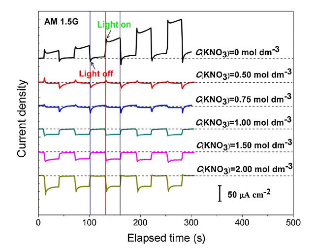
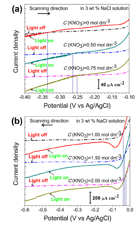
Fig. 4 showed photocurrent responses of Cu2O films at the open circuit potential (-0.17 V) in a 3 wt% NaCl solution. Anodic photocurrents, corresponding n-type semiconducting behavior, were generated for the Cu2O films formed in the plating solutions with 0 - 0.75 mol dm-3 KNO3. The unstable anodic photocurrent in Fig. 4 was due to the oxidation from Cu2O to CuO [27] as showed in the optical pictures of electrodes in Fig. S6 in Supporting Information. The Cu2O films behaved as p-type semiconductors when KNO3 concentration was from 1.00-2.00 mol dm-3. The cathodic photocurrent intensity increased gradually as KNO3 concentration increased. Fig. 4 and Fig. S6 show that photoelectrochemical stability of Cu2O films exhibited a significantly improvement as the conductivity trasformed from n-type to p-type.
Fig. 4. Zero-bias photocurrent characterization for Cu2O films grown in the plating solutions with varying concentrations of KNO3.
The voltammograms under illumination (100 mW cm-2) and dark of all Cu2O films were measured in 3 wt% NaCl solution, as shown in Fig. 5. To avoid large overpotential oxidizing n-type Cu2O or reducing p-type Cu2O in advance during photo-voltammogram measurement, the scanning direction was set from negative to positive for n-type Cu2O and from positive to negative for p-type Cu2O films. It can be seen from Fig. 5, the onset potentials of the Cu2O films were shifted to positive potential with increasing the KNO3 concentration in the plating solution. The onset potential variation is consistent with the flat band potentials change obtained from the Mott-Schottky analysis. The conductivity types, onset potentials, flat band potentials and carrier densities of Cu2O films obtained through different methods were summarized in Table 1. Generally, the carrier densities (1017-1019 cm-3) of p-type Cu2O films grown on Cu substrates (by thermal oxidation, chemical oxidation or comproportionation) were higher than that (1015-1017 cm-3) of p-type Cu2O films grown on conductive glass substrate (ITO or FTO) by electrodeposition. Variability of carrier densities for n-type Cu2O films fabricated by different methods is similar with that for p-type Cu2O films. The results indicate that higher carried densities could be obtained by growing Cu2O film from Cu substrate, compared to depositing Cu2O film from Cu2+ solution. Although there is no exact matching for the onset potential or flat potential of the Cu2O films in this work compared to previous reports because of the influence of electrolyte and carrier density, it shows that n-type Cu2O film with higher carrier density has a negative onset potential or flat potential, and p-type Cu2O film with higher carrier density has a more positive onset potential or flat potential [12,13].
Fig. 5. Voltammograms under illumination (100 mW cm-2) and dark of Cu2O films formed in the plating solutions with varying concentrations of KNO3.
3.3.1. Growth of Cu2O film by comproportionation
During the comproportionation (as presented in Eq. (1) [11,14,15]), the metallic Cu behaves as the reducing agent to form Cu+ from the Cu2+ ions present in solution. Hence the growth of Cu2O films by comproportionation could be regarded as two stages. At the first stage (Stage I), the interface is Cu/solution before Cu2O completely covered Cu substrates. At the second stage (Stage II), Cu2O films have entirely covered Cu substrates and Cu/Cu2O/solution junctions are formed. Fig. 6 shows growth diagrams of the two stages in comproportionation to obtain Cu2O film.
Fig. 6. Growth diagrams of Cu2O films by comproportionation. (a) Cu foil was immersed in the plating solution; (b) Cu2O crystals grew as islands on the Cu subtrates; (c) a layer of Cu2O film formed and covered Cu substrate completely; (d) Cu2O film increased thickness with oxidized Cu substrate and reduced Cu2+ from the plating solution.
When Cu foil was immersed in the plating solution, the comproportionation occurred spontaneously as the Fermi level energy (-4.65 eV vs. vacuum [28]) of metallic copper is higher than the electrochemical potential of plating solution (-4.942 eV vs. vacuum [29], 0.245 V vs. Ag/AgCl(Sat. KCl) electrode in 0.1 mol dm-3 CuSO4 solution).
Cu+Cu2++H2O→Cu2O+H+ (1)
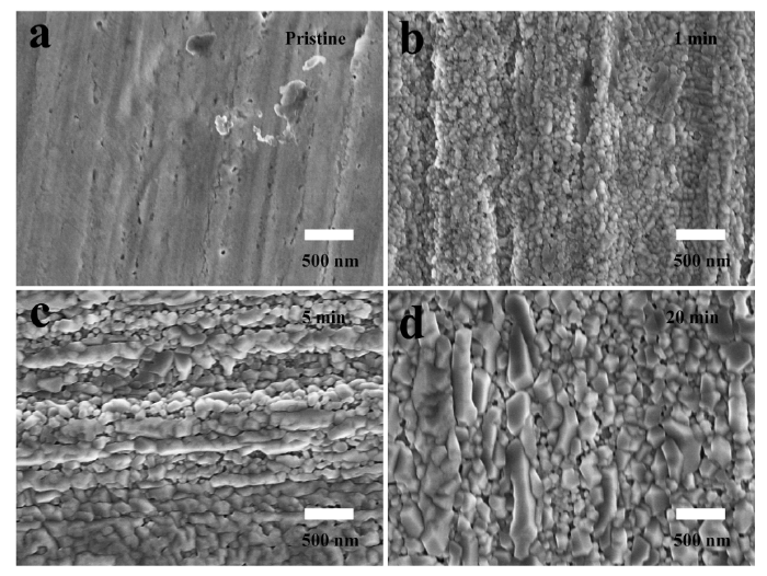
During stage I, Cu2O crystals first grew sparsely on the copper substrate (Fig. 6(a, b)), while the unreacted metallic copper continued to react with Cu2+ continuously untill Cu2O crystals contacted each other to cover the entire Cu substrate in the plating solution (Fig. 6(c)). Fig. 7 shows SEM images of Cu2O films grew by comproportionation for different times in the plating solutions. It could be seen that Cu2O film thoroughly covered the surface of Cu foil, which reacted for only 1 min. The comproportionation could be decomposed into three sub-reactions at different inerfaces as shown in Eqs. (1a-1c) (the subscripts of Cu and Cu2+ indicate the Cu+ coming from metallic copper and plating solution, respectively). Eqs. (1a) and (1b) present the oxidation of metallic copper and the reduction of Cu2+, respectively. Eq. (1c) shows that one Cu+ formed from the Cu foil and one Cu+ from Cu2+ in solution combined with O2- from OH- to form Cu2O.
Cu-e-→Cu+(Cu) (1a)
Cu2++e-→Cu+(Cu2+) (1b)
Cu+(Cu)+Cu+(Cu2+)+H2O→Cu2O+2H+ (1c)
Fig. 7. SEM images of Cu2O films prepared by comproportionation for varying times in the plating solutions without KNO3.
At stage II, the metallic copper no longer contacts the plating solution, such that the electrons provided by copper have to pass through the Cu2O layer to reach the Cu2O/solution interface. At this interface, new Cu2O formed by the reaction of Cu2+ and OH- in the plating solution as presented in Eq. (1d). Meanwhile, O2- ions in the Cu2O bulk moved from the Cu2O/solution interface to the Cu/Cu2O interface to combine the new Cu+ generated from copper due to an oxidative step as shown in Eq. (1e) (Fig. 6(d)). Consequently, Cu2O film grew at both the Cu2O/solution interface and the Cu/Cu2O interface simultaneously and increased in thickness as the comproportionation continued.
Cu+(Cu2O)+e-+Cu2++H2O→Cu2O+2H+ (1d)
2Cu+(Cu)+O2-(Cu2O)→Cu2O (1e)
3.3.2. Tuning conductivity type of Cu2O film by comproportionation
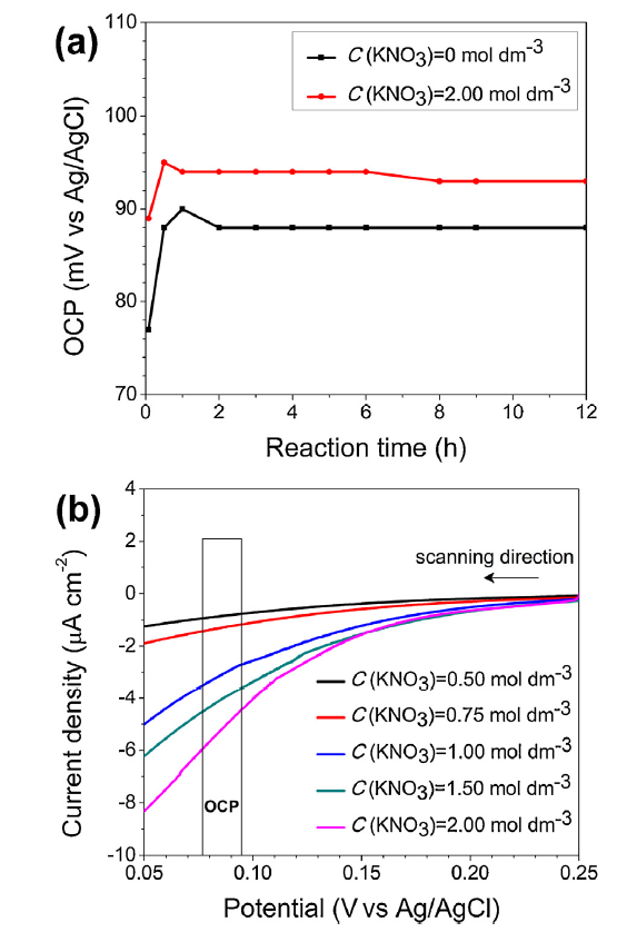
The open current potentials (OCP) of copper foil in the plating solution with and without KNO3 during the growth of Cu2O films were measured (Fig. 8(a)). In the initial comproportionation (1 h), the OCP is increased because there are more cations (such as Cu2+ and Cu+) accumulated on the surface of copper foil. After comproportionation for 1 h, the change in OCP is small (<15 mV). The OCP results suggested that the comproportionation was similar to a potentiostatic process and the oxidation ability of plating solution was enhanced (the OCP increased) because of the addition of KNO3. Therefore, when KNO3 was added into the plating solution, the reduction of NO3- ions (Eq. (2)) occurred during comproportionation because the equilibrium potential of the reaction presented by Eq. (2) was 0.356 V (pH 5.00, with 0.5 mol dm-3 KNO3), which was more positive than OCPs (0.077-0.95 V, Fig. 8(b)) of the copper foils in the plating solution. Hence the reduction of NO3- ions took place spontaneously.

Fig. 8. (a) OCPs of Cu foil in the plating solutions without KNO3 and with 2.00 mol dm-3 KNO3 for growing Cu2O film during comproportionation; (b) polarization curves of Pt foil in KNO3 solution without CuSO4 (pH=5.00). The counter eletrode was another Pt foil.
To investigate the reduction of NO3- ions, the polarization behavior of Pt foils in KNO3 solutions (pH = 5.00) without CuSO4 were measured and showed in Fig. 8(b). It can be seen that the reduction current densities of NO3- ions became larger with increasing NO3- concentration at range of OCPs. Thus, the reduction of NO3- ions could occur and compete with the reduction of Cu2+ ions at the interface of Cu2O/solution. The supression of reduction of Cu2+ ions could produce Cu vacancies in Cu2O film and cause the change of the conductivity type [30]. In addition, as shown in Eq. (2), reduction of NO3- ions consumes H+ in solution, leading to pH increase at the interface of Cu2O/solution. The increased pH affected both the growth and the conductivity transformation of Cu2O films. The thicknesses of Cu2O films prepared from plating solution containing different concentration of KNO3 were measured (Fig. S7 in Supporting Information). The thickness of Cu2O film increased from 3.9 μm to 8.2 μm as the NO3- concentration increased from 0 to 2.00 mol dm-3. This could be attributed to that the more consumed H+ ions facilitated the comproportionation to grow Cu2O according to Eq. (1). Meanwhile, the concentration of hydroxide ions increased (i.e., pH increased) with H+ ions being consumed at the interface of Cu2O/solution, hence the supply of hydroxide ions became sufficient (relative to the reduction from Cu2+ to Cu+) for the growth of Cu2O film, producing more Cu vacancies in Cu2O film. This result confirmed that the increased concentrations of KNO3 consume more H+ from solution, leading to the change of pH at the interface of Cu2O/solution interface. The mechanism of tuning conductivity type of Cu2O film through comproportionation by controlling KNO3 concentration was illustrated in Fig. 9.
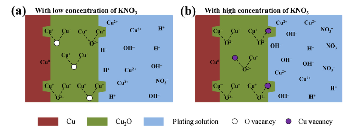
Fig. 9. Mechanism of controlling conductivity type of Cu2O film through comproportionation by changing the concentration of KNO3 in plating solutions. (a) Rich oxygen vacancies formed in Cu2O film at low concentrations of KNO3 due to the local acid environment at Cu2O/solution interface, and (b) rich copper vacancies formed in Cu2O film at high concentrations of KNO3 owing to reduction of NO3- consuming more H+, leading to a basic local environment at Cu2O/solution interface.
When KNO3 concentrations were lower than 0.75 mol dm-3, the local environment at the Cu2O/solution interface was acidic and oxygen vacancies were formed in Cu2O film [31]. This corresponded with the observed n-type conductivity. With the increase of KNO3 concentration in the plating solution, the n-type behavior became weak due to the decrease of donor density in Cu2O films (Table 1). When the KNO3 concentrations were higher than 1.00 mol dm-3 in the plating solution, more H+ was consumed and the local pH at Cu2O/solution interface increased. The basic local environment at the Cu2O/solution interface resulted in sufficient OH- ions to grow Cu2O films rich in Cu vacancies giving rise to the observed p-type conductivity [[32], [33], [34], [35]]. In previous studies [26,[32], [33], [34], [35]], tuning conductivity type of Cu2O films was realized by controling the pH of plating solution during electrodeposition. In such treatments, p-type Cu2O films was electrodeposited in basic solution, that was because sufficient OH- in the solution could provide enough O to facilitate the growth of Cu2O films and form Cu vacancies. On the contrary, n-type Cu2O film was electrodeposited in acidic solution, due to the supply of O is unsufficient during the growth of Cu2O films and O vacancies were formed. Therefore, the mechanism proposed in this work is analogous to that proposed by controling solution pH during electrodeposition.
This work illustrated a simple and general method that tuning the conductivity type of Cu2O through comproportionation by adding appropriate amount of oxidizing agent. As an example, we briefly investigated the formation of Cu2O films formed by the reaction of Cu foils with cupric ions in the presence of potassium permanganate Fig. S8 in Supporting Information). The role of the permanganate ions is to control the local pH by consuming H+ in the dilute acid plating solution. This further demonstrates that this type of comproportionation is applicable beyond our nitrate plating solution and is a truly general method.
Cu2O films were grown through comproportionation by immersing copper foil in dilute acid CuSO4 solution and the conductivity types of Cu2O films were modulated by adding different concentrations of nitrate ions. The effect of KNO3 concentration on the surface morphology, phase structure, chemical composition and optical performance of Cu2O films was small. The PEC experiments demonstate that the Cu2O films behave with n-type and p-type conductivity for films grown in plating solutions with nitrate ion concentrations ≤0.75 and ≥1.00 mol dm-3, respectively. Mott-Schottky results indicate that with increasing nitrate ions concentration in plating solution, the carrier densities of n-type Cu2O films decreased, while that of p-type Cu2O films increased. As a consequence, the flat band potentials of Cu2O films became more positive. The growth of Cu2O films by comproportionation could be considered as two stages, the isolated Cu2O crystals formed on Cu substrates in Stage I and Cu2O films completely covered Cu substrates in stage II as indicated by SEM observation of films formed at different growth time. When KNO3 concentrations are low (≤ 0.75 mol dm-3), the local environment at the Cu2O/solution interface is acidic and the supply of OH- is insufficient, hence rich oxygen vacancies are formed in the Cu2O film, resulting in n-type conductivity. When the KNO3 concentrations are high (≥1.00 mol dm-3), much more H+ in the plating solution were consumed and the local pH at Cu2O/solution interface becomes more basic. Sufficient OH- are supplied to grow Cu2O films and rich Cu vacancies were formed in film leading to p-type conductivity. These results demonstrate a new methodology of forming Cu2O/Cu interface films, as well as an in-depth investigation into the growth processes and mechansim. In the future, this method could be used to fabricate homojunction electrode on metal substrate for PEC or photoelectric application.
This work was financially supported by the National Natural Science Foundation of China (No. 51302216 and 21375102). Ying Yang thank the Excellent Young Academic Backbone Program of the Northwest University, the Open Fund of the State Key Laboratory of Multiphase Flow in Power Engineering of China and the Scientific Research Program funded by Shaanxi Provincial Education Department (No. 17JS121). The “Top-rated Discipline” construction scheme of Shaanxi higher education in China supported part of this work. The authors acknowledge Mr. Matthew Hautzinger from the Department of Chemistry, University of Wisconsin-Madison to improve the quality of the manuscript.
Supplementary material related to this article can be found, in the online version, at doi:https://doi.org/10.1016/j.jmst.2019.04.009.
The authors have declared that no competing interests exist.

 WeChat
/
| 〈 |
|
〉 |
