Search for articles:
Xiaohan Li , Zhidong Zhang
Corresponding authors:
Copyright: 2019 Editorial board of Journal of Materials Science & Technology Copyright reserved, Editorial board of Journal of Materials Science & Technology
More
Abstract
Modulating the ferroelectric properties of P(VDF-TrFE) polymers both electrically and optically could open up new opportunities for their applications in non-volatile memories and sensors. Here by using the Nb:SrTiO3 semiconductor as electrode compared with metal Au electrode, we report on the modulation of ferroelectric properties of P(VDF-TrFE) thin film capacitors both by electric field and UV light. A ferroelectric hysteresis loop shift together with the asymmetric switching behavior has been observed when using semiconducting electrode, which could be explained by the band alignment model based on interfacial charge screening. On the basis of band bending near the ferroelectric/semiconductor interface, we could further modulate the ferroelectric switching behaviors reversibly by UV light illumination. Our research provides a new route to engineer the ferroelectric properties of P(VDF-TrFE) polymer thin film capacitors, promising their applications in optoelectronic devices.
Keywords:
Due to their respectable piezoelectric and pyroelectric properties, as well as the low-cost, flexible, and environment-friendly features, organic ferroelectrics have great potential to be used in modern applications such as flexible electronics, photovoltaic devices and artificial skins [[1], [2], [3], [4], [5]]. Compared with other organic ferroelectrics [6,7], P(VDF-TrFE) (70:30) polymer has large remanent polarization (Pr$\widetilde{8}$.5 μC/cm2) [8], relative high Curie temperature (Tc $\widetilde{3}$62 K) [9] and good piezoelectric properties (d33˜ -35 pm/V) [10]. However, one drawback of P(VDF-TrFE) polymers is their relatively high coercive field (>50 MV/m relevant to film thickness and working frequency) [11,12], which is 10$\widetilde{1}$00 times stronger compared with that of ferroelectric ceramic counterparts [[12], [13], [14]]. To extend their application into low-voltage driven non-volatile memories, we need to find effective ways to modulate the coercive field and switching time while maintain the remanent polarization. For the inorganic ceramic counterparts, several ways have been explored for this purpose, including the strain engineering for BaTiO3 [15,16] and BiFeO3 [13] epitaxial thin films, the electrostatic coupling between defect-dipoles and polarization for BiFeO3 films [17,18], the interface engineering for PZT thin films [19], and recently the optical modulation in BaTiO3/MoS2 heterostructures [20]. However, these routes have been rarely explored for the organic ferroelectrics, especially for P(VDF-TrFE) polymer. Strain engineering is not feasible for P(VDF-TrFE) polymer, because the soft polymers have a big mismatch with the commonly used rigid substrates which will block the effective strain transfer between substrates and polymer films. The defect-polarization electrostatic coupling is weak considering that the defects in P(VDF-TrFE) polymers are mainly molecule mis-alignment, which is neutral and cannot interact with ferroelectric polarizations electronically [11]. Although charged defects could be introduced manually by electric method or ion irradiation [21,22], it tends to destroy the molecule alignment seriously and results in tiny remanent polarization. Compared with these routes, interface engineering between ferroelectric and electrodes could be a feasible way for hysteresis-loop modulation of P(VDF-TrFE) polymers. This is based on the fact that different electrodes, such as semiconductors and metals, can have different charge screening abilities [23]. The asymmetric electrodes could provide an additional electric potential that superimposed onto the depolarization field, thus can modulate the switching behavior of ferroelectrics [24,25]. This should generally work both for inorganic and organic ferroelectrics. Considering metal electrodes have been mainly used in the research of the P(VDF-TrFE) thin film capacitors in the past years, it will be interesting to investigate the semiconductor/P(VDF-TrFE) interface, and to check how the electrical properties of electrodes affect the ferroelectric properties of P(VDF-TrFE) polymer thin films.
In this work, by using Nb doped SrTiO3 semiconductor of different doping levels as electrodes, we have explored this issue systematically. We found that the ferroelectric properties such as ferroelectric loop and switching dynamics of P(VDF-TrFE) polymers could be modulated by the selection of electrodes. In addition, the excellent UV light absorption [26] of Nb:SrTiO3 and the semi-transparent nature [27] of P(VDF-TrFE) polymer films offer us a good chance to modulate the electric properties of P(VDF-TrFE) polymer films by 365 nm UV light. Our research thus provides a feasible way to engineer the ferroelectric properties of P(VDF-TrFE) thin films both electrically and optically.
Firstly, P(VDF-TrFE) (70/30 mol% VDF/TrFE) powder (Piezotech S. A.) was dissolved in diethyl carbonate and stirred at 60 ℃ for 1 h to form a solution with a concentration of 6 wt.%. The solution was then filtered by passing through a PTFE pore with diameter of 0.45 μm. P(VDF-TrFE) thin films were then prepared by spin coating at 3000 rpm for 35 s on Nb:SrTiO3 (NSTO) (001) single crystal substrates (with Nb doping concentration of 0.05 wt.%, 0.1 wt.%, and 0.5 wt.%, respectively), and also on Au(120 nm)/Ti(10 nm)/SiO2 substrate for comparison, followed by annealing at 140 ℃ for 2 h to enhance the crystallinity as reported before [28]. For the ferroelectric and electric test, 150 nm thick Cu top electrodes with a size of 200 μm in diameter were deposited onto the film by thermal evaporation.
To confirm the crystallization of P(VDF-TrFE) film, X-ray diffractometer (XRD, Bruker AXS D8 DISCOVER) was used, and the surface morphology was investigated by atomic force microscopy (AFM, Bruker Dimension Icon). Ferroelectric characterizations including polarization hysteresis loop and switching dynamics were carried out by ferroelectric tester (Precision Multiferroic, Radiant Technology). Ferroelectric properties were also investigated by piezoresponse force microscope (PFM, Bruker Dimension Icon) with Pt/Ir-coated Si cantilever tips. In typical PFM measurements, an AC voltage of amplitude of 3000 mV and at a contact resonance frequency of $\widetilde{3}$00 kHz was applied on the tip. Electrical properties were investigated on a probe station equipped with a sourcemeter (Keithley 2400). For light response test, a UV light source with a wavelength of 365 nm and beam size of Φ4 mm (SUVF, Agiltron) was used. All tests were carried out at room temperature and the positive voltage corresponds to the current flowing from top electrode to bottom electrode.
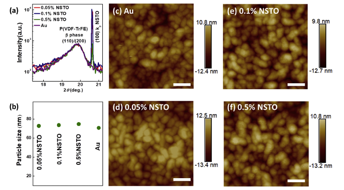
P(VDF-TrFE) molecular has two typical chain conformations including TGTG (gauche) and TTTT (all trans), corresponding to non-polar α phase and polar β phase, respectively [29]. The film inclines to form polar β phase when introducing TrFE units [30]. Fig. 1(a) shows the XRD patterns of our P(VDF-TrFE) films spin-coated on different substrates including Au/Ti/Si and NSTO with thickness of $\widetilde{2}$76 nm (Supporting information Fig. S1). All the films show the same diffraction peak positioned at 2 θ = 19.8°, which belongs to the (200)/(110) crystalline plane of β phase. This suggests that the as-prepared thin films have the crystalline β phase with the same orientation, independent on the substrates of Au and NSTO. This is further supported by the AFM images as shown in Fig. 1c-f, where all the films share similar surface morphologies with the same and uniform particle size distribution (Fig. 1b). The root-mean-square roughness of four samples is 4.1 nm, 5.1 nm, 3.4 nm, and 4.6 nm (Fig. S1), respectively, indicating the high quality of the films. These investigations suggest that different substrates used here have minor effect on the structural crystallinity and homogeneity of spin coated P(VDF-TrFE) polymer films. If there is some difference in their ferroelectric properties, it will be largely an electronic effect correlated with the interfaces of Au/ P(VDF-TrFE) or NSTO/ P(VDF-TrFE) rather than the difference between P(VDF-TrFE) thin films themselves.
Fig. 1. Structure and morphology characterization: (a) XRD pattern of P(VDF-TrFE) film on different substrates (Au, 0.05% NSTO, 0.1% NSTO, and 0.5% NSTO substrate.) (b) Particle size of P(VDF-TrFE) crystalline on different substrates. (c), (d), (e), (f) AFM morphology images of P(VDF-TrFE) copolymer films on different substrates. Scale bars, 200 nm.
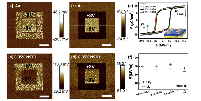
We use the piezoresponse force microscopy (PFM) to investigate the local ferroelectric properties of the P(VDF-TrFE) thin films. As shown in Fig. 2a-d, obvious amplitude and phase contrast were observed after writing square patterns with opposite voltages of +8 V and -8 V through the PFM tip, indicating the ferroelectric nature of the P(VDF-TrFE) thin films on Au and NSTO substrates. From amplitude response images (Fig. 2a & b), we can see films on Au substrate shows equal amplitude response for opposite domains with a clear domain wall boundary (Fig. 2a). Whereas amplitude response of the opposite domains for film on NSTO substrate is asymmetric (Fig. 2b), i.e., the amplitude of +8 V region is larger than that of -8 V region. Such a difference could be due to the different electric boundary conditions experienced by the two films. Au substrate and Pt coated PFM tip have similar work functions ($\widetilde{5}$.2 eV and $\widetilde{5}$.6 eV, respectively), and minor electric potential and electrostatic effect is expected, the amplitude response is thus intrinsic and symmetric. However, the electron affinity of NSTO is $\widetilde{3}$.9 eV [31], so an electric potential difference as large as $\widetilde{1}$.7 eV exists between NSTO and Pt electrodes. This would contribute a large electrostatic effect into the piezoresponse signal, resulting in the asymmetric piezo-response behavior. Such an electrostatic effect has been observed before for bare NSTO substrate [31]. The electrostatic effect could also affect the phase contrast of opposite domains, which is $\widetilde{9}$0° for film on Au substrate and reduces to $\widetilde{4}$6° for that on NSTO substrate (Supporting information Fig. S2).
Fig. 2. Ferroelectric hysteresis loops and coercive fields of devices: (a), (b) PFM amplitude image and (c), (d) phase image of square domains on Au and 0.05% NSTO substrates with opposite domains written by a PFM tip with alternate voltage of +8 V and -8 V. Scale bars, 2 μm. (e) P-E loops of P(VDF-TrFE) films on different substrates (f) Coercive field for P(VDF-TrFE) films.
To determine the ferroelectric properties quantitatively, typical ferroelectric hysteresis loops (P-E) at room temperature and at 100 Hz have been investigated for the capacitor devices fabricated on different substrates as shown in Fig. 2e. The schematic device structure is shown in the inset. All the devices show similar P-E loops with remanent polarization Pr of 7.3$\widetilde{8}$.2 μC/cm2, and P-E loop of Au/PVDF/Cu device is a little slimmer compared with that of NSTO/PVDF/Cu device. Quantitatively, the coercive field of P(VDF-TrFE) film on Au substrate is 5.4 MV/m lower than that on NSTO substrates. This result suggests that it is easier to switch devices on Au substrates. In addition, a minor difference between positive coercive field (Ec+) and negative coercive field (Ec-) has been observed for all devices, which is generally due to the imprint effect of the as-grown P(VDF-TrFE) thin films [11,32,33].
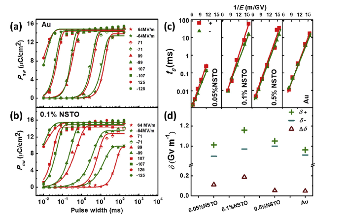
To investigate the switching dynamics of P(VDF-TrFE), a positive-up-negative-down (PUND) method with a five-consequent pulse voltage sequence [11] was applied onto the devices and the switched polarization Psw was recorded accordingly. The pulse width ranges from 0.01 ms to 100 ms. Fig. 3a and b shows Psw on typical substrates of Au and 0.1% NSTO, respectively. Both positive (red data) and negative (green data) electric field have been applied. For samples on Au substrate, the switching behaviors under positive and negative electric fields show minor difference. This is due to the relative symmetric electrodes that have been used, which results in the symmetric switching to the electric field. Note that both Au and Cu are good conductors with similar conductivity (254.5 S/cm for Cu and 308.6 S/cm for Au). For samples on 0.1%NSTO substrate, it shows an obvious asymmetric switching behavior under opposite electric fields. We can see that a longer pulse width is required to induce the same Psw for a positive electric field, compared with that of using negative electric field. For example, the device starts to switch at $\widetilde{1}$ ms for -64 MV/m, whereas it starts to switch at $\widetilde{1}$0 ms for +64 MV/m. Similar asymmetry has also been observed under other electric fields, indicating that P(VDF-TrFE) thin film is easier to switch under negative electric field when prepared on NSTO substrate. Such a difference between devices on Au (Fig. 3a) and on NSTO (Fig. 3b) suggests that the semiconducting nature of NSTO electrode could affect the switching dynamics of P(VDF-TrFE) effectively. We will discuss the possible mechanisms in the next section.
Fig. 3. Switching dynamics of P(VDF-TrFE) thin films on different substrates: Switched polarization Psw as a function of pulse width at different external fields on typical substrates of (a) Au and (b) 0.1% NSTO, respectively. The red data and green data are obtained under positive voltage and negative voltage, respectively. Solid lines are the fittings according to KAI model. (c) Switching time to versus 1/E on various substrates. (d) Activation field δ+ and δ- under positive and negative voltages obtained from (c) for films on different substrates, Δδ is the difference of δ+ and δ-.
To quantify the switching dynamics of P(VDF-TrFE) thin films, we use the Kolmogorov-Avrami-Ishibashi (KAI) model [34] to fit the data in Fig. 3a and b. KAI theory assumes a homogeneous nucleation and unrestricted domain growth, which is suitable for describing P(VDF-TrFE) polymer thin films [11] and other inorganic ceramic thin films [35,36] with the following equation,
Psw(t)=2Pr[1-exp(-(t/t0)n)] (1)
where t is the pulse width, Psw(t) is the switched polarization, Pr is the remanent polarization, t0 is the switching time constant, and n is the geometric dimension for domain growth. Solid lines in Fig. 3a, b and Fig. S3 are the fitting results according to Eq. (1), which is in good agreement with the experimental data. The fitted switching time constant t0 versus the inverse of electrics field 1/E for different samples are shown in Fig. 3c, which conforms to Merz’s law [37] very well with the following expression:
to=t∞exp(δ/E) (2)
where δ is the activation field and t∞ is the lower limit of switching time that can be extracted from the slope and intercept of curve respectively [38]. The corresponding activation field δ+ (δ-) under positive (negative) electric field directions on various substrates are summarized in Fig. 3d. Generally, the sample on Au substrate possesses a modest activation field (+0.96 GV/m and -0.91 GV/m) compared with that on NSTO substrate, consistent with the fact that P(VDF-TrFE) is easier
to be switched on Au substrate (Fig. 2). And the asymmetry of the activation field is larger for samples on NSTO substrate compared with that on Au substrate, especially for low doping level of 0.1% and 0.05%. A deep doping up to 0.5% will induce a highly conducting electrode interface, which results in the similar behavior as that of using Au electrode. This suggests that the semiconducting nature of NSTO could affect the switching properties of P(VDF-TrFE) capacitors effectively.
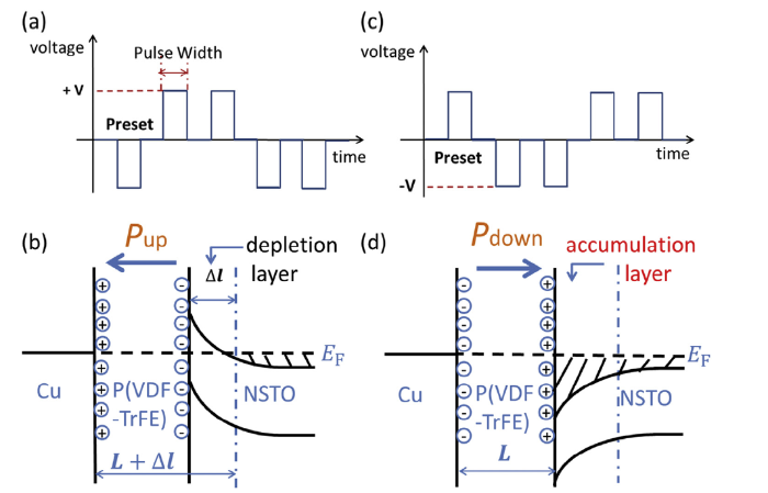
We propose a possible explanation for the electrode effect on switching dynamics of P(VDF-TrFE) thin films. The fact that both films on conducting Au and semiconducting NSTO substrates share the same structural crystallinity, similar crystalline distribution and topography suggests that it is mainly an electronic effect from the electrode. To illustrate this point, the band alignment model is shown in Fig. 4.
Fig. 4. Band model analysis of the semiconducting electrode effect on switching dynamics of P(VDF-TrFE) thin film capacitors: (a) The voltage-pulse sequence of PUND test for a positive electric field. (b) The corresponding band alignment of Cu/P(VDF-TrFE)/NSTO structure before the test in (a). (c) The voltage-pulse sequence of PUND test for a negative electric field. (d) The corresponding band alignment of the device before the test as-shown in (c).
As we know, NSTO is an n-type degenerate semiconductor, and its charge screening ability is not as brilliant as metal like Au and Cu [26] because of low carrier density. When NSTO is in contact with P(VDF-TrFE), a good insulator with a large band gap of $\widetilde{6}$ eV [39], a band bending occurs near the NSTO interface, with the bending direction depending on the polarization state of P(VDF-TrFE). Note that the band bending on metallic Cu or Au electrode could be ignored due to their high carrier densities and excellent charge screening abilities with a very short screening length of less than one angstrom [23]. During the PUND test for a positive electric field (Fig. 4a), a negative preset voltage will be applied onto the device which puts the polarization state pointing upwards the top Cu electrode (Pup) as shown in Fig. 4b. This will drive the NSTO surface into a depletion state, with a depletion length Δl, to screen the negative polarization charges at the interface of P(VDF-TrFE)/NSTO. For example, based on the charge neutralization condition, Δl is estimated to be $\widetilde{3}$0 nm for 0.05 wt.% NSTO and decreases to $\widetilde{3}$ nm for 0.5 wt.% NSTO, depending on doping induced carrier density (Supporting Note). Due to the insulating nature and longer effective working thickness (L + Δl) of depletion region, we need a stronger positive electric field or a longer pulse time to switch Pup. On the contrary, when the initial polarization points to NSTO substrate (Pdown, Fig. 4d), NSTO will be driven into an accumulating state and behaves like a metal. In this case, the effective working thickness is L, and a smaller negative electric field or shorter electric pulse width is required to switch Pdown. This makes Pup more stable compared with Pdown and could explain the positive shift of P-E loops (Fig. 2) and the asymmetric switching dynamics (Fig. 3) for samples prepared on NSTO substrate. We thus conclude it is the polarization dependent electronic state of NSTO that turns back to affect the switching properties of P(VDF-TrFE) thin films.
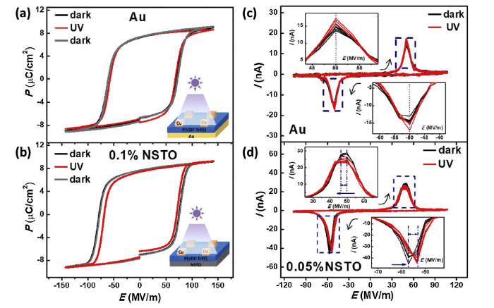
NSTO is also a good light absorber [26], which provides an additional chance to modulate the ferroelectric properties of P(VDF-TrFE) thin film capacitors by light illumination. Such a modulation has been achieved in ferroelectric ceramic thin film before [20,26], but seldom for ferroelectric polymers. Fig. 5a and b illustrates the P-E hysteresis loops in the dark and under UV light illumination (wavelength 365 nm, light intensity $\widetilde{5}$.0 W/cm2) for P(VDF-TrFE) thin film capacitors on Au and NSTO substrates, respectively. As can be seen, there is minor change in P-E loops in dark, during and after UV light illumination for devices on Au substrate. By contrast, slim P-E loop with distinct reduced coercive field has been induced by UV light illumination for device on NSTO substrate (Fig. 5b). e.g., Ec decreases from 78.3 MV/m to 64 MV/m with a change of 18% has been observed, and residual polarization is consistent with that before UV light illumination. To avoid the light induced heating effect, nitrogen gas was guided across the device surface during the measurement, and a slight temperature increase of $\widetilde{3}$ °C was monitored under UV light illumination, which would have minor effect on the as-observed coercivity reduction. The fact that minor change occurs for Au based device also excludes the possible heating effect.
Fig. 5. Light modulation on ferroelectric switching of P(VDF-TrFE) thin film capacitors: (a) and (b), P-E hysteresis loops in the dark and under UV light illumination for P(VDF-TrFE) thin film capacitors on Au and 0.05% NSTO electrodes, respectively. (c) and (d) the corresponding switching I-V curves in the dark and under UV light illumination. Insets: enlarged region near the switching current peaks.
Such a coercivity reduction was also observed in the static I-V measurement as shown in Fig. 5c and d. Two current peaks originate from the switching of the polarization during the voltage sweeping process. The enlarged current peak region (inset of Fig. 5d) clearly reveals that there is a peak shift to lower electric field for I-V curves under UV light illumination for P(VDF-TrFE) on NSTO substrate, i.e., +Ec reduces from 50 MV/m to 46 MV/m and -Ec reduces from -57 MV/m to -53 MV/m, which results in an average coercivity reduction by $\widetilde{8}$% after light illumination. This value is smaller than that of $\widetilde{1}$8% observed in the P-E loops as shown in Fig. 5b. This is due to the fact that transient switching current measurements are done in the quasi-static frequency region ($\widetilde{0}$.08 Hz), while the P-E loops are characterized under frequency of 100 Hz. On the contrary, there is no peak shift for P(VDF-TrFE) on Au substrate (Fig. 5c), which collaborates with minor change of P-E loops shown in Fig. 5a. To avoid any intrinsic imprint effect [32,33], a training procedure up to 20 cycles has been performed to achieve a stable polarization switching curve before the light illumination. Similar UV light illumination modulated coercivity was also observed on other samples prepared on NSTO (0.01% NSTO, 0.5% NSTO) substrates (see Supporting Information Figs. S4, S5), suggesting it is a common feature of using NSTO electrode. We thus believe that it is closely related with the electronic properties of NSTO substrate. The 365 nm UV light with photon energy of $\widetilde{3}$.4 eV could induce a band-to-band excitation in NSTO electrode (bandgap$\widetilde{3}$.1 eV) [26] and produce a large amount of electrons and holes near the NSTO/ P(VDF-TrFE) interface. These free carriers could reduce the depletion or even enhance the accumulation of NSTO interface, making the electric field applied onto P(VDF-TrFE) more effectively and reducing the electric field required for polarization switching. Note that a Cu top electrode with a thickness of $\widetilde{1}$50 nm has been applied in the present case, which will block most of the UV light. So NSTO will mainly absorb the UV light from the side and the light effect is moderate. To improve the light modulation ability in future, a transparent top electrode could be considered carefully, which should have a processing temperature lower than 140 °C to avoid damage to the P(VDF-TrFE) thin films. Suitable candidate include silver nanowires embedded into poly(4,3-ethylene dioxythiophene): poly(styrene-sulfonate) (PEDOT:PSS) [40].
In summary, by using semiconductor Nb:SrTiO3 as electrode, we could tailor the ferroelectric properties of P(VDF-TrFE) thin film capacitors effectively. The asymmetric P-E loops and switching dynamics could be well explained by a simple band alignment model, which is based on the polarization dependent electronic states of NSTO/ P(VDF-TrFE) interface. In addition, the semiconducting nature of NSTO also allows us to modulate the ferroelectric loop of P(VDF-TrFE) capacitors through light illumination for the first time. A coercivity change up to $\widetilde{1}$8% is realized by a 365 nm light illumination. Our experiment results may open doors towards the light sensors or light modulated memories based on ferroelectric polymers in the future.
This work was supported by the “Hundred Talents Program” of Chinese Academy of Sciences (CAS).
Supplementary material related to this article can be found, inthe online version, at doi:https://doi.org/10.1016/j.jmst.2019.05.040.

 WeChat
/
| 〈 |
|
〉 |