
Tungsten Doped Indium Oxide Thin Films Deposited at Room Temperature by Radio Frequency Magnetron Sputtering
[Pan Jiaojiao, Wang Wenwen*  , Wu Dongqi, Fu Qiang, Ma Ding]
, Wu Dongqi, Fu Qiang, Ma Ding]
|
|


Tungsten doped indium oxide (IWO) thin films were deposited on glass substrate at room temperature by radio frequency reactive magnetron sputtering. Chemical states analysis was carried out, indicating that valence states of element W in the films were W4+ and W6+. The effects of sputtering power and film thickness on the surface morphology, optical and electrical properties of IWO thin films were investigated. The IWO thin films had high transmittance in near infrared (NIR) spectral range. The resistivity, carrier mobility and carrier concentration owned their respective optimum values as sputtering power and thickness changed. The as-deposited IWO film with the minimum resistivity of 3.23 × 10⁻⁴ Ω cm was obtained at a sputtering power of 50 W, with carrier mobility of 27.1 cm2 V-1 s-1, carrier concentration of 7.15 × 1020 cm-3, average transmittance about 80% in visible region and above 75% in NIR region. It may meet the application requirement of high conductivity and transparency in NIR wavelength region.
Transparent conductive oxides are widely used in various applications such as in flat panel display, light emitting diodes and photovoltaic cells [1], [2], [3] and [4]. It is well known that the visible light (400–700 nm) accounts for only 43% of the energy in the air-mass 1.5 global solar irradiance spectrum (300–2500 nm), and near infrared (NIR, 700–2500 nm) region occupies 52% and ultraviolet (300–400 nm) 5% of the radiation [5] and [6]. However, all commonly used transparent conductive oxides (TCO) thin films including In2O3:Sn (ITO), SnO2:F, and ZnO:Al as transparent window electrodes of solar cells suffer from the free carrier absorption in the NIR region, limiting the long-wavelength response of solar cells [1]. According to the Drude model, the increase of the transparency to NIR without compromising the conductivity can only be achieved by increasing the mobility and decreasing the carrier density [7] and [8]. Tungsten doped indium oxide (In2O3:W, IWO) is a promising material for optoelectronic and photovoltaic application due to its low electrical resistivity, high electron mobility and high transparency in both visible and NIR region [9].
It has been shown in previous studies that IWO thin film prepared by direct current (DC) magnetron sputtering technique requires a substrate temperature above 300 °C [9] and [10]. Gupta et al. [10] and Zhang et al. [11] and [12]have reported the effect of thickness on optical and electrical properties of IWO films by DC magnetron sputtering at 500 and 380 °C, respectively. It was also found that W6+ can supply three extra electrons when it substitutes In3+. As a result, with fewer doping ratio of W ions, the IWO films can achieve a rather high conductivity and transparency in the NIR range because of higher carrier mobility. The doping ratio is usually lower than 6 wt% in IWO while in the preparation of ITO, the value is about 10 wt% [1], [2] and [3].
In this work, in order to meet the requirement of sputtering the IWO film on flexible substrate with temperature no more than 100 °C, the deposition of IWO thin films by radio frequency (RF) magnetron sputtering under room temperature was realized by using a ceramic target. The doping content of tungsten in the target is chosen to be 4.8 wt%. This doping content is determined through previous experiments which indicate that 6 wt% is acceptable and an even lower value could also be tested [8], [9] and [10]. The influences of sputtering power and film thickness on the crucial properties of IWO thin films are investigated.
Films of polycrystalline IWO were prepared by RF magnetron sputtering using ceramic targets (60 mm (diameter) × 3.5 mm (thickness), purity of 99.99%, 4.8 wt% W-doped In2O3) at room temperature. A vacuum vessel with a volume of 0.1 m3 was evacuated by a molecular pump, which resulted in a base pressure of 1 × 10⁻³ Pa before introducing pure argon and oxygen gas [13]. The oxygen partial pressure of the vessel was maintained at 4 × 10⁻³Pa using a needle valve and the working pressure was maintained at 1 Pa during the film deposition. The distance between the target and the substrate was kept at 75 mm. The IWO film was deposited on glass substrate which was mounted on a circular cathode. A grounded metal ring served as the main anode [14], [15] and [16]. Two groups of IWO thin films using different sputtering power varying from 40 to 90 W and different sputtering time to get film thickness distributed from 110 to 360 nm were obtained, respectively.
The thicknesses of films were measured with α step profiler (Dektak6M). The crystallinity was evaluated by grazing-incidence X-ray diffraction (XRD, Rigaku D/max-2200pc). The surface morphology was imaged by scanning electron microscopy (SEM, BACPCS4800). Surface roughness was measured through atomic force microscopy (AFM, Nanosurf Easyscan 2). The element profile of the film was measured by X-ray photoelectron spectroscopy (XPS). The optical transmittance spectra were measured by spectrophotometer. The carrier mobility and concentration of IWO films were characterized with Hall effect measurements using the van der-Pauw technique [7] and [17].
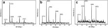
Fig. 1 shows the XRD patterns of IWO thin films prepared at oxygen partial pressure of 4 × 10⁻³Pa with different sputtering power. It is obvious that the IWO thin film is polycrystalline, with each identified diffraction peak being consistent with cubic bixbyite In2O3structure. Within the resolution threshold of the instrument, no peaks of impurities phase can be detected from the films, implying that the tungsten doping will not change the crystalline structure of indium oxide. The radius of In3+and W6+are 0.081 and 0.065 nm, respectively, thus the doped tungsten ion can substitute indium in the lattice of In2O3. The strongest diffraction peak of the film deposited under 50 W corresponds to the (222) plane and the grain size is estimated to be 90 nm using the Debye–Scherrer formula from the half maximum width of the (222) peaks [18] and [19]. It can be found in Fig. 1 that with increasing sputtering power, the crystallinity is firstly improved and decreases. On the other hand, the preferred orientation changes gradually, with the strongest diffraction peak turning from (222) plane to (400) plane.
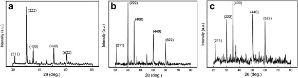 | Fig. 1. XRD pattern of IWO film deposited at room temperature with different sputtering power of 50 W (a), 80 W (b), 90 W (c) and the same deposition time of 25 min. |
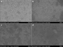
Fig. 2 shows the SEM images of the surface morphology of IWO films with different sputtering power of 40, 50, 80 and 90 W and the sputtering time of 25 min. It can be found that all samples have smooth surface, and the preferred orientation changes gradually with increasing sputtering power, corresponding with the XRD results shown in Fig. 1 and related analysis in Section. Comparing with the scale, the changing tendency of the grain size is also in agreement with the calculation mentioned in Section. Through AFM measurement, the surface roughness (root mean square, RMS) of IWO thin films is 1.09, 2.69, 4.27 and 4.72 nm, when the sputtering power is 40, 50, 60 and 80 W, respectively.
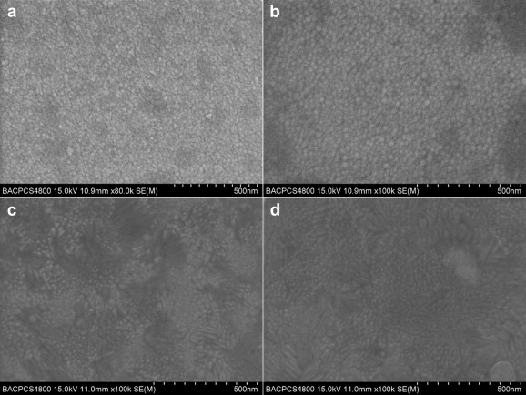 | Fig. 2. SEM images of IWO thin films deposited at room temperature with different sputtering power of 40 W (a), 50 W (b), 80 W (c), 90 W (d) and the same deposition time of 25 min. |
In order to identify the chemical states of indium and tungsten elements in the IWO films, the representative XPS survey for the film was performed, and the results are shown in Fig. 3. Fig. 3(a) and (b) exhibit the spectra of In 3 d and W 4 f , respectively. The spectrum of In 3 d consists of a doublet with binding energies of 444.4 eV for the In 3 d5/2and 451.8 eV for the In 3 d3/2, corresponding to the binding energies of the In3+ion in In2O3. Doublet with binding energies of 35.2 eV for the W 4 f7/2and 37.6 eV for the W 4 f5/2is found in the spectrum of W 4 f , which implies that the tungsten atoms are oxidized to W6+and W4+ions during the deposition process. Additional peaks around 530.6 and 284.6 eV are related to O 1 s and C 1 s signal, respectively [20] and [21]. The oxidation process can easily happen at a high temperature with incorporation of oxygen, but at room temperature the process cannot be fully completed. The results also confirm the high valence difference between the doped and substituted ions in the IWO thin films.
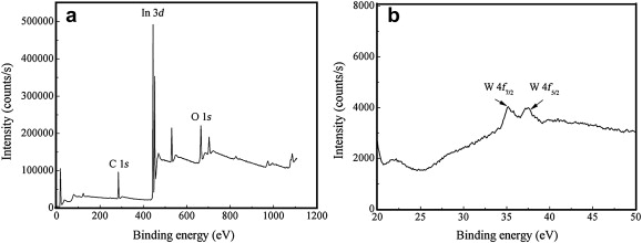 | Fig. 3. XPS spectra of the IWO film deposited at room temperature. |
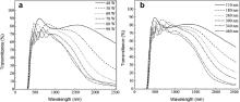
Fig. 4(a) shows the optical transmittance spectra of IWO films deposited on glass substrates with different sputtering power. The sputtering power is found to strongly affect the optical transmittance of these films. It can be seen that the films which are deposited at 40–50 W have higher transparency both in visible and NIR region. In the range of 400–2200 nm, the average transparency of the films grown at room temperature with a sputtering power of 40 W is 78%, and the average transparency in visible region is over 85%.
 | Fig. 4. (a) Optical transmittance spectra of the IWO films prepared with different sputtering power and the same deposition time of 25 min, (b) optical transmittance spectra of the IWO films deposited with different thickness and the same sputtering power of 60 W. |
Fig. 4(b) shows the effect of film thickness on optical transmittance of IWO films. The film thickness is controlled and adjusted by deposition time. All films are highly transparent in visible and NIR region and the transparency of the films decreases as the thickness of the films increases. The average transparency of the films with a thickness of 180 nm is over 80%.
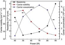
The dependences of electrical resistivity, carrier concentration and mobility on the sputtering power are exhibited in Fig. 5. The electrical resistivity of IWO films is determined by taking the product of sheet resistance and film thickness. The carrier concentration ( n) is derived from the relation n = 1/( eRH), where RH is the Hall coefficient and e is the absolute value of the electron charge. The carrier mobility ( μ) is determined by the relation μ = 1/( nρe), where ρ is the resistivity. Fig. 5 shows that the resistivity of IWO films decreases from 6.48 × 10⁻⁴Ω cm to the minimum value (3.23 × 10⁻⁴Ω cm) when the sputtering power increases from 40 to 50 W and then it grows to 9.01 × 10⁻⁴Ω cm at 90 W. It can also be found that after a small increase, the carrier mobility of IWO thin film decreases sharply from 27.1 to 14.1 cm2V-1s-1 as the sputtering power increases from 50 to 90 W. On the other hand, the carrier concentration increases from 3.66 × 1020cm-3 at the sputtering power of 40 W to the maximum of 9.25 × 1020cm-3 at 70 W, then it drops to 4.94 × 1020cm-3at 90 W.
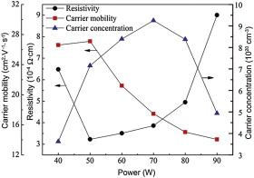 | Fig. 5. Dependences of electrical resistivity, carrier concentration and mobility of IWO films on sputtering power. |
It is known that a high conductivity is resulted from high carrier concentration and mobility. Consequently, the minimum resistivity is obtained when the sputtering power is 50 W, where the carrier mobility has the maximum value and the concentration is also acceptable. At the beginning, as sputtering power increases, the carrier concentration also increases due to the growing of the thickness and the modification of the crystallinity. However, it is presumed that when the sputtering power is too large, incomplete substitution of indium ions by tungsten ions could happen because of the high speed of film deposition, which probably results in the decrease in the carrier concentration [22]. On the other hand, when the sputtering power is larger than 50 W, the carrier mobility shows a sharp decline when the power increases, which can be explained with the following theory. When sputtering power is excessively high, incomplete oxidation may cause a large amount of defects and clubbed nano-wire monocrystallines which have loose arrangement, resulting in an increase of grain boundary scattering and leading to the drop of carrier mobility [22]. This explanation can be supported by XRD analysis which indicates that the films deposited at low sputtering power are more crystalline when the sputtering power is over 50 W.
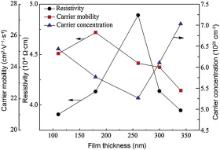
Fig. 6 shows the influence of the thickness on the electrical resistivity, carrier concentration and carrier mobility of IWO films deposited at room temperature. As shown in the graph, the electrical resistivity firstly increases then decreases as the thickness grows from 100 to 350 nm. The changing tendency is resulted from the joint changes of carrier concentration and mobility. With increasing thickness from 100 to 250 nm, the carrier concentration of IWO films drops. However, after 250 nm, the further increase of the thickness leads to a rise of carrier concentration. When the film thickness is small, the rather short deposition time could result in more oxygen vacancies, so when the deposition time increases, the number of oxygen vacancy decreases, leading to the decrease in the carrier concentration. At the same time, as deposition time grows, the substrate temperature also increases because of the continuous collisions by the sputtered target atoms and ions. Higher substrate temperature could enhance the substitution of In3+ions by W ions, resulting in the rise of carrier concentration after 250 nm. On the other hand, the carrier mobility has an opposite change tendency to carrier concentration with the top value 26.2 cm2V-1s-1obtained at 180 nm. Migration rate is influenced by both grain boundary scattering and film surface scattering. Polycrystalline films with small grains are mainly controlled by the grain boundary scattering, and carrier mobility increases when grain size becomes larger. When the film is thinner, the grain is smaller, and the function of grain boundary scattering and film surface scattering is stronger, which lead to a lower mobility. As the film thickness increases, its crystallization is improved, the growth of grain size weakens intergranular scattering and prolongs the service life of the carrier, therefore the carrier mobility increases. With the further increase of the thickness, once the grain size of the film exceeds a certain value, it will be no longer dominated by the grain boundary scattering. Meanwhile the increase of film thickness also reduces the surface electric field effect. With the influence of oxygen vacancy and the doping of W ions, the migration rate declines when the thickness of IWO film is larger than 180 nm.
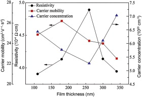 | Fig. 6. Electrical resistivity, carrier concentration, and carrier mobility of IWO films with different thickness. |
Transparent conductive oxide thin films of tungsten doped In2O3 with high transparency in NIR region have been deposited on conventional glass substrates by RF magnetron sputtering at room temperature. These films are highly transparent and conductive with high mobility. The lowest resistivity of 3.23 × 10⁻⁴Ω cm is obtained when the sputtering power is 50 W with the carrier concentration of 7.15 × 1020cm-3and carrier mobility reaching the maximum value of 27.1 cm2V-1s-1. At the same time, the average transmittance of the film is about 75% in NIR region and 80% in visible region. The results indicate that IWO thin films deposited at room temperature have a performance advantage for applications where high conductivity and transparency in NIR wavelength region are required.
This work was financially supported by the National Natural Science Foundation of China (No. 50902006) and Aviation Science Foundation of China (2012zf51066).
| 1. |
|
| 2. |
|
| 3. |
|
| 4. |
|
| 5. |
|
| 6. |
|
| 7. |
|
| 8. |
|
| 9. |
|
| 10. |
|
| 11. |
|
| 12. |
|
| 13. |
|
| 14. |
|
| 15. |
|
| 16. |
|
| 17. |
|
| 18. |
|
| 19. |
|
| 20. |
|
| 21. |
|
| 22. |
|