Search for articles:
Shuan Li , Xingguo Li
Corresponding authors:
Received: 2019-03-8
Revised: 2019-04-16
Accepted: 2019-04-30
Online: 2019-10-05
Copyright: 2019 Editorial board of Journal of Materials Science & Technology Copyright reserved, Editorial board of Journal of Materials Science & Technology
More
Abstract
Gadolinium oxide (Gd2O3) film has potential as a candidate gate dielectric to replace HfO2. In this work, we provide a simple method by trace Ta ($\widetilde{1}$%) doping to significantly improve the dielectric properties of Gd2O3 film. And effects of annealing temperatures of Ta-doped Gd2O3 (GTO) films are investigated in detail. Results show that GTO film annealed at 500 °C exhibits excellent performance as a novel gate dielectric material for integrated circuit, showing a small surface roughness of 0.199 nm, a large band gap of 5.45 eV, a high dielectric constant (k) of 21.2 and a low leakage current density (Jg) of 2.10 × 10⁻³ A/cm2. All properties of GTO films are superior to pure Gd2O3 films and these GTO films meet the requirements for next-generation gate dielectrics. In addition, impedance spectrum is first used to analyze the equivalent circuit of GTO based metal-oxide-semiconductor (MOS) capacitors, which represents a new insight to understand observed electrical behaviors.
Keywords:
Complementary metal-oxide-semiconductor field effect transistors (CMOSFETs) are the key basic units for integrated circuits [[1], [2], [3], [4]]. Furthermore, the core structure of CMOSFETs is gate dielectric [5]. In past ten years, the greatest breakthrough in gate dielectric for integrated circuit development is the replacement of SiO2 and polysilicon gate electrodes by high dielectric constant (k) metal oxides and metal gate electrodes [6]. Among them, the function of high k metal oxides is to maintain the same capacitance by keeping the film physical thickness thicker [7]. High k materials make it possible to downscale electronic devices and integrate more functions for future integrated circuits [[8], [9], [10]].
As we known, HfO2 based high k oxides have become a new generation of gate dielectric for electronic devices since 2007 [11], because there are many advantages of HfO2, such as a relatively large band gap ($\widetilde{5}$.5 eV), a relatively large dielectric constant (k$\widetilde{2}$0) and a large band gap offset to Si substrates [[12], [13], [14], [15], [16]]. However, HfO2 is not perfect and also has its own shortcomings. Firstly, some reports have indicated that the crystallization temperature of pure HfO2 is lower than 500 °C [17]. Secondly, HfO2 cannot effectively prevent the diffusion of oxygen, causing oxygen from gate dielectric to react with substrate to form a low-k layer [18,19]. In order to deal with these problems, on the one hand, people try their best to improve the performance of HfO2 by doping, etc [18,[20], [21], [22], [23], [24]]. On the other hand, people are dedicated to finding new high k metal oxides to replace HfO2 [25,26]. In this work, we focus on looking for potential high k gate dielectrics.
Among all candidate oxides, Gd2O3 attracts more and more attention, due to its suitable band gap (>5 eV), high chemical and thermal stability with Si and extremely higher crystallization temperature (>1000 °C) than HfO2 [[27], [28], [29]]. However, its dielectric constant is relatively small (k<18) [28]. In this work, we offer a simple method by Ta doping via magnetron co-sputtering method to improve the performance of Gd2O3 film. And annealing temperature effects of Ta-doped Gd2O3 (GTO) films on microstructure, optical and electrical properties are comprehensively studied. Finally, impedance spectrum is first used to analyze GTO based metal-oxide-semiconductor (MOS) capacitors annealed at different temperatures, which offers a new insight into electrical behaviors of GTO thin films.
Ta-doped Gd2O3 thin films were prepared on clean quartz glass substrates or Si wafers by radio frequency (RF) sputtering method. The sputtering power of both gadolinium target (99.95%, Ф50 mm × 4 mm) and yttrium target (99.95%, Ф50 mm × 4 mm) was set to 30 W. Base chamber pressure was fixed to 5 × 10⁻⁴ Pa at least and the mass flow of Ar and O2 was controlled to 30:10 sccm to ensure that the working pressure during film deposition was maintained at $\widetilde{0}$.6 Pa. As a comparison, pure Gd2O3 films were deposited by RF sputtering a Gd target with the power of 30 W.
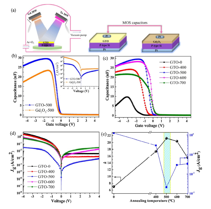
The measurement of capacitance-voltage (C-V) curves, the leakage current density -voltage (I-V) curves and impedance spectrums are based on MOS capacitors. As shown in Fig. 1, $\widetilde{2}$0 nm GTO or Gd2O3 high k films were deposited on p-type (100) Si wafers with a resistivity of 1-10 Ω cm. Then $\widetilde{6}$00 nm Pt electrodes were deposited on the back of Si wafer and surface of high k oxides films by a direct current (DC) sputtering of 70 W. The area of Pt electrodes (3.14 × 10⁻² cm2) was determined by shadow masks. Finally, all GTO films were annealed in pure oxygen atmosphere (100 sccm) for 6 min at temperatures of 0, 400, 500, 600 and 700 °C, respectively. In order to highlight the advantages of Ta incorporation, pure Gd2O3 film was annealed at 500 °C for the same annealing process. All samples were marked as GTO-T or Gd2O3-T (T stands for temperature from 0 to 700 °C) in following discussion.
Fig. 1. Flow chart for preparation of MOS capacitors.
The composition of the GTO film was determined by inductively coupled plasma-atomic emission spectrometer (ICP: Prodigy 7). The microstructure of GTO and Gd2O3 film was characterized by scanning electron microscopy (SEM, Hitachi S4800), transmission electron microscopy (TEM: JEOL JEM-2100), X-ray diffraction equipment (XRD, PANalytical X’Pert3 Powder) and atomic force microscope (AFM, SPI3800/SPA400). The optical properties of GTO and Gd2O3 films were measured by UV/Vis spectrometer (Lambda 35). The electrical properties of GTO and Gd2O3 film were measured by precision LCR meter (TH2838 H) and electrochemical workstation (CHI760D). The impedance spectrums of GTO films were measured by electrochemical workstation (CHI760D).
The atomic ratio of Ta to (Ta + Gd) is determined by ICP method and can be extracted to be 1%. The initially deposited GTO film is an amorphous film, which is consistent with XRD patterns of the GTO-0 thin films in Fig. 2(f). As observed by SEM (Fig. 2(b)), the thickness of the film used to test electrical properties and impedance spectrum is about 20 nm. And EDS mapping of GTO film demonstrates the average and uniform distribution of Ta and Gd atoms. Fig. 2(f) shows the XRD patterns of the GTO thin films as a function of annealing temperatures. All GTO films annealed at 400 to 700 °C are in amorphous states, due to the extremely high crystallization temperature of Gd2O3 (in our experiments, the Gd2O3-900 film is still amorphous). There are many advantages to use amorphous oxides over polycrystalline oxides. First, defects are more likely to occur at the oxide grain boundaries, which will reduce the performance of thin films [30]. Second, the grain boundaries always act as paths of leakage current density and doping elements, such as B or P from Si wafers [31,32]. Third, since the amorphous oxide and its dielectric constant are isotropic, the polarization fluctuation of the oxide does not cause the carriers to scatter around [11]. In this work, the crystallization temperature of ternary GTO thin films exceeds 700 °C at least, which is higher than HfO2 films crystallized at 500 °C [17] and their TiO2-doped HfO2 films crystallized at 600 °C [18].
Fig. 2. (a) TEM image of $\widetilde{5}$ nm GTO-0 film, (b) SEM image of GTO film thickness for electrical performance test, (c, d, e) EDS mapping of GTO-0 thin films and (f) XRD patterns of GTO and Gd2O3 thin films.
AFM images of GTO and Gd2O3 films are shown in Fig. 3(a)-(f). Compared with Fig. 3(a) and (d), surface roughness (Ra) of GTO film (0.199 nm) is smaller than pure Gd2O3 film (0.213 nm), implying that Ta doping improves the surface quality of Gd2O3 films, which may be attributed to that proper incorporation of Ta can change Gd2O3 film growth mode [33]. When it comes to annealing temperature effect on GTO film surface morphology, as shown in Fig. 3(g), Ra of GTO-0, GTO-400, GTO-500, GTO-600 and GTO-700 films are 0.402, 0.248, 0.199, 0.203 and 0.443 nm, respectively. Obviously, when annealing temperature is increased to 500 °C, the GTO film exhibits the smoothest surface (0.199 nm), which is ideal for suppressing leakage current caused by surface roughness [10,34]. However, accompanying annealing temperature from 500 to 700 °C, the values of Ra have a significant increase from 0.199 to 0.443 nm, which may be ascribed to higher temperature causing the aggregation of oxide particles and local crystallization of the GTO film. However, no peak is observed by XRD patterns, indicating that the film may be slightly crystallized locally [35]. As shown in Fig. 3(f), the surface of the GTO-700 film does have some raised small particles, confirming the guess above.
Fig. 3. AFM images of (a) Gd2O3-500 film, (b, c, d, e, f) GTO-T film and (g) Ra of Gd2O3-500 and GTO-T (T = 0, 400, 500, 600 and 700 °C) films.
High k oxide film should have a large enough band gap to act as an insulator in CMOSFETs, so it is necessary to measure band gaps of GTO thin films. In this work, we measure the optical absorption of GTO and Gd2O3 films deposited on quartz glass substrates by UV-vis spectroscopy. Based on optical absorption of GTO and Gd2O3 films, the band gaps can be determined by Tauc method [[36], [37], [38]]. In this study, the band gap of pure Gd2O3 film is determined to be 5.27 eV. It is noteworthy that GTO film has a higher band gap (5.47 eV) than pure Gd2O3 film. Based on the previous study, the band gap of pure Ta2O5 film is only $\widetilde{4}$.5 eV [11,39]. However, the doping of Ta can increase the band gap of Gd2O3 film. As we known, Ta2O5 is a n-type semiconductor whose incorporation causes the Fermi level to enter the conduction band, so that electrons can only be excited to the upper level of the Fermi level, resulting in GTO film exhibiting a larger band gap than pure Gd2O3 film [11,40]. As shown in Fig. 4(b), accompanying temperature from 0 to 500 °C, the absorption of GTO films increases from 0.25 to 0.35. However, the absorption of the GTO film is slightly decreased to 0.31 when annealing temperature reaches 700 °C, this can be attributed to higher surface roughness causing photon scattering [41]. Correspondingly, as shown in Fig. 4(c)-(g), the band gaps of GTO-0, GTO-400, GTO-500, GTO-600 and GTO-700 films are 5.25, 5.30, 5.45, 5.37 and 5.34 eV, respectively. Based on the previous studies [11,42], the band offset of the high k oxide film relative to Si (the band gap of Si (Eg) is 1.12 eV) substrate should be greater than 1 eV. Considering that the conduction band offset is usually less than the valence band offset, the band gap of the candidate oxide film should exceed 5 eV [11,40]. All band gaps of GTO films, especially GTO films annealed at 500 °C (5.45 eV), fulfill this requirement.
Fig. 4. (a) Optical absorption and band gap of Gd2O3-500 film, (b) optical absorption and (c, d, e, f, g) Tauc plots of GTO-T (T = 0, 400, 500, 600 and 700 °C) films and (h) band gaps of Gd2O3-500 and GTO-T (T = 0, 400, 500, 600 and 700 °C) films (α: absorption coefficient; h: Planck constant; υ: frequency of light).
As shown in Fig. 5(a), to highlight the advantages of Ta doping, we compared the k values and leakage current density (Jg) of GTO-500 and pure Gd2O3-500 samples. In terms of C-V curves (Fig. 5(b)), based on the accumulation data of C-V curves, dielectric constants of samples can be calculated [15,43]. The k values of Gd2O3-500 and GTO-500 samples are determined to be 16.8 and 21.2, respectively. The result indicates that incorporation of Ta into Gd2O3 film can effectively improve the dielectric constant, one reason is that $\widetilde{1}$% Ta doped Gd2O3 film has fewer defects (such as oxygen vacancies) than pure Gd2O3 film. Flat band voltage (Vfb) can reflect the defects generated in films and large negative Vfb shift can be attributed to the presence of oxygen vacancies and the interface state [30,44]. By Ref. [45], the flat band voltages (Vfb) of GTO-500 and Gd2O3-500 samples are calculated to be -0.13 and -0.28 V, respectively. Therefore, GTO film has fewer defects and exhibits a higher dielectric constant. Another reason is that, according to the phase diagram of Gd2O3 and Ta2O5 [46], a Gd3TaO7 phase (k>200) may be formed in GTO film, which can increase the dielectric constant of GTO film [47]. In terms of I-V curves, incorporation of Ta into Gd2O3 film can decrease leakage current density from 0.146 to 2.10 × 10⁻³ A/cm2 at (Vfb-1) V. Therefore, we conclude that proper incorporation of Ta ($\widetilde{1}$%) into Gd2O3 film is beneficial for improving its dielectric properties.
Fig. 5. (a) Schematic diagram of magnetron co-sputtering GTO film as well as GTO and Gd2O3 based MOS capacitors, (b) C-V and I-V curves of GTO-500 and Gd2O3-500 samples, (c) C-V, (d) I-V curves and (e) k value and Jg value change chart of GTO-T (T = 0, 400, 500, 600 and 700 °C) samples.
Fig. 5(c) shows the C-V points of Pt/GTO-T/Si/Pt MOS capacitors (T = 0, 400, 500, 600 and 700 °C). The dielectric constant can be calculated to be 7, 17.4, 21.2, 20.4 and 15.6 for GTO-0, GTO-400, GTO-500, GTO-600 and GTO-700 samples, respectively. The dielectric constant of annealed GTO samples is greatly improved compared to as-deposited samples. The value of Vfb of GTO-0, GTO-400, GTO-500, GTO-600 and GTO-700 samples are determined to be -1.77, -0.68, -0.13, 0.16 and 0.21 V, respectively. Vfb of GTO films gradually increases from -1.77 to 0.21 V from 0 to 700 °C, indicating that higher temperature annealing leads to lower density of oxygen vacancies and defects in GTO film. The other parameters of the GTO and Gd2O3 films obtained from the C-V curves are summarized in Table 1.
Table 1 Parameters extracted from C-V curves (Cox: accumulation capacitances; Cfb: flat band capacitance; Qox: equivalent oxide-charge density; EOT: equivalent oxide thickness).
| Sample | Cox (nF) | k | Cfb (nF) | Vfb (V) | Qox (cm-2) | EOT (nm) |
|---|---|---|---|---|---|---|
| GTO-700 | 24.09 | 15.6 | 2.04 | 0.21 | 2.83×10¹² | 5 |
| GTO-600 | 28.29 | 20.4 | 2.07 | 0.16 | 3.60×10¹² | 3.8 |
| GTO-500 | 29.46 | 21.2 | 2.07 | -0.13 | 5.45×10¹² | 3.7 |
| GTO-400 | 24.15 | 17.4 | 2.04 | -0.68 | 1.29×10¹² | 4.5 |
| GTO-0 | 9.72 | 7.0 | 1.81 | -1.77 | 4.97×10¹² | 11.1 |
| Gd2O3-500 | 23.40 | 16.8 | 2.04 | -0.28 | 5.03×10¹² | 4.6 |
Fig. 5(d) shows the leakage current density of GTO films. The leakage current density (Jg) of GTO-0, GTO-400, GTO-500, GTO-600 and GTO-700 samples is 1.253, 0.297, 2.10 × 10⁻³, 2.92 × 10⁻² and 3.40 × 10⁻² A/cm2 at (Vfb-1) V. It is obvious that GTO-500 samples have the lowest leakage current density, which corresponds to the GTO-500 sample with the smoothest surface (0.199 nm) and largest band gap (5.45 eV) among all GTO-T films. Fig. 5(e) shows the k values and Jg values of GTO films as a function of annealing temperature. As a result, we confirm that the best annealing process for GTO film is annealing at 500 °C in O2 atmosphere, which can provide a reference for the high-k rare earth oxides annealing process.
Impedance spectrum analysis is an effective way to help us better understanding electrical behavior of electronic devices, such as lithium storage process of lithium battery [48]. However, no work takes advantage of impedance spectrum to analyze the electrical performance of MOS capacitors. In this work, we focus on the response of impedance spectrums to GTO-400, GTO-500, GTO-600 and GTO-700 samples. This method can provide a direct evidence to explain the difference in leakage current density between four samples. The frequency of the impedance spectrum is chosen to be 10-2-106 Hz. The Nyquist plots of GTO-400, GTO-500, GTO-600 and GTO-700 samples are displayed in Fig. 6(a). It is noteworthy that every MOS capacitor exhibits a depressed semicircle, which corresponds to the polarization process of GTO gate dielectric. However, the intercept of the semicircle in the real axis is significantly different, which means that the resistances in the Pt/GTO/Si/Pt MOS capacitors are different. Fig. 6(b) reveals two time constants appearing during the test, implying that there are two RC elements connected in series in Pt/GTO/Si/Pt MOS capacitors [49]. By fitting the above spectrum with Zview software, the equivalent circuit can be described in the inset of Fig. 6(c), which includes a series resistor R1 and a constant phase angle element CPE2 in parallel with the resistor R2. The total impedance can be written as follows [50]:
Z=R1+ $\frac{1}{\frac{1}{R^{2}}j\omega CPE_{2}}$ (1)
where j is a constant and ω is angular frequency. By fitting impedance spectrum, as shown in Fig. 6(d)-(g), several key parameters can be extracted and listed in Table 2. The values of resistor R1 are similar for four samples ($\widetilde{5}$0 Ω) and R1 can be attributed to external test systems, such as test equipment and fixtures. But the values of R2 are completely different for GTO-0, GTO-400, GTO-500, GTO-600 and GTO-700 samples and R2 is the contribution from internal resistance of MOS capacitors, which is one of the key factors affecting the electrical performance of MOS capacitors. As displayed in Fig. 6(h), R2 of GTO-400 sample is 3156 Ω. And GTO-500 samples show the largest value of R2 (5272 Ω). However, the values of R2 decrease from 5272 to 576.6 Ω while annealing temperature increasing from 500 to 700 °C. Obviously, the trends of leakage current density and R2 value with annealing temperature are opposite, which is consistent with the conclusion that the larger the resistance value, the smaller the leakage current density, that is, GTO-500 sample has the smallest leakage current density, probably due to its largest R2 value.
Fig. 6. (a) Nyquist plots, (b, c) θ and |Z| as a function of frequency (the inset in (c) shows the equivalent circuit), (d, e, f, g) fitting curves of GTO-400, GTO-500, GTO-600 and GTO-700 samples and (h) values of R2 as a function of annealing temperature (Z’: real part of impedance; Z’’: imaginary part of impedance; θ: phase angle).
Table 2 Parameters extracted from equivalent circuit.
| Sample | R1 (Ω) | R2 (Ω) | CPE2-T (F) | CPE2-P |
|---|---|---|---|---|
| GTO-700 | 49.37 | 576.6 | 1.88×10⁻⁷ | 0.77 |
| GTO-600 | 50.79 | 3004 | 7.37×10⁻⁸ | 0.82 |
| GTO-500 | 49.97 | 5272 | 4.62×10⁻⁸ | 0.83 |
| GTO-400 | 51.38 | 3156 | 2.87×10⁻⁹ | 0.91 |
A novel high k gate dielectric is successfully fabricated by Ta doped Gd2O3 film via magnetron co-sputtering method. Trace Ta doping can significantly improve the performance of Gd2O3 films. And the GTO films annealed at 500 °C exhibit superior performance to HfO2 for candidate gate dielectric materials, such as the largest dielectric constant of 21.2 and the smallest Jg value of 2.10 × 10⁻³ A/cm2. Such excellent performance of GTO-500 film is attributed to its amorphous structure, minimum surface roughness (Ra = 0.199 nm), largest band gap (5.45 eV) and fewer defect density. Besides, we first used the impedance spectrum to creatively analyze the equivalent circuit of MOS capacitors, which offers a direct evidence to explain the observed electrical behaviors as function of annealing temperature. Therefore, the simple preparation method and excellent performance will enable GTO films to be the next generation gate dielectric materials.
This work is supported financially by the Project of Ministry of Science and Technology of the People's Republic of China (No. 2017YFB0405902), the National Natural Science Foundation of China (Nos. 51431001, 51771002, 21771006, U1607126 and 21621061) and Beijing Municipal Commission of Science and Technology (No. Z17110000091702).

 WeChat
/
| 〈 |
|
〉 |


