Short-Term Synaptic Plasticity Mimicked on Ionic/Electronic Hybrid Oxide Synaptic Transistor Gated by Nanogranular SiO2 Films
[Zhaojun Guo1, 2 , Liqiang Guo2 , Liqiang Zhu2, *  , Yuejin Zhu
1 ]
, Yuejin Zhu|
|


An indium-zinc-oxide (IZO) based ionic/electronic hybrid synaptic transistor gated by field-configurable nanogranular SiO2 films was reported. The devices exhibited a high current ON/OFF ratio of above 107, a high electron mobility of ∼14 cm2 V−1 s−1 and a low subthreshold swing of ∼80 mV/decade. The gate bias would modulate the interplay between protons and electrons at the channel/dielectric interface. Due to the dynamic modulation of the transient protons flux within the nanogranular SiO2 films, the channel current would be modified dynamically. Short-term synaptic plasticities, such as short-term potentiation and short-term depression, were mimicked on the proposed IZO synaptic transistor. The results indicate that the synaptic transistor proposed here has potential applications in future neuromorphic devices.
Inspired by the high efficiency of neural computation in biological systems, neuromorphic computational systems based on solid-state neural network have attracted much attention[1], [2] and [3]. Electrically triggered memristors with self-learning abilities were proposed to mimic the synaptic behaviors in biological systems and were reported to have potential applications in neuromorphic computation[4], [5], [6] and [7]. The field-driven migration of metal ions results in the formation of metal filaments and the decreased resistivity. Transistors, with several unique characteristics, are also pretty candidates for emulating artificial synapses and thus for building artificial neural networks. Alibart et al.[8] reported pentacene-based organic transistor behaving as an artificial synapse to mimic short-term plasticity of a biological synapse. Synaptic transistors with p-Si channel and carbon nanotube (CNT) have also been investigated to mimic signal processing and learning functions[9] and [10]. Much attention has been attracted on zinc oxide based semiconductors. Structure and electrical characteristics were studied[11], [12] and [13]. Especially, amorphous oxide semiconductor-based thin-film transistors (TFTs) have stimulated considerable attention due to their high electron mobility and low processing temperature[14], [15] and [16]. However, there are few reports on amorphous oxide semiconductor-based transistors for mimicking biological synaptic plasticity. It is well known that low-dimensional inorganic semiconductor nanostructures are attracting tremendous interest due to their unique physical and chemical properties[17] and [18]. Recently, nanogranular SiO2 films have also been proposed as a solid-state electrolyte to gate the oxide semiconductor, resulting in metal-insulator phase transition[19]. Due to the unique protonic/electronic coupling effects within the nanogranular SiO2 electrolyte, nanogranular SiO2 electrolyte gated transistor has been proposed to mimic the synaptic responses[20] and [21]. In this work, we demonstrated that analog synaptic plasticity behaviors can be mimicked in an indium-zinc-oxide (IZO) based thin-film transistors fabricated at room temperature. The gate bias modulated the interplay between protons and electrons at the channel/nanogranular SiO2 film interface. Typical transistor characteristics and short-term synaptic plasticities were obtained. The proposed synaptic transistor has potential applications in future neuromorphic devices.
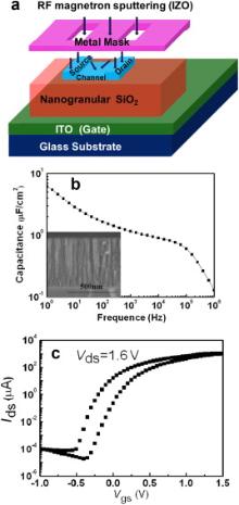
Fig. 1 (a) shows the schematic diagram for obtaining IZO thin-film transistors (TFTs) on indium-tin-oxide (ITO) coated glass substrates. Firstly, a phosphorus (P)-doped nanogranular SiO2 layer was deposited on ITO glass substrates by plasma enhanced chemical vapor deposition (PECVD) by using SiH4/PH3mixture (95% SiH4 + 5% PH3) and O2 as reactive gases. Then, patterned IZO layers (150 μ m × 1000 μ m) were deposited on the nanogranular SiO2 by radio frequency (RF) magnetron sputtering with a nickel shadow mask. The nickel shadow mask was placed above the substrate. The deposition was performed using IZO ceramic target (In2O3:ZnO = 90:10 in wt%) sputtered with a RF power of 100 W. The working pressure and Ar gas flow rate were set to 0.5 Pa and 14 sccm (standard cubic centimeter per minute), respectively. As shown in Fig. 1(a), the sputtered IZO nanoclusters will diffract into the shadow regions of the nickel mask. Therefore, a thin IZO channel layer will be self-assembled between two patterned IZO layers simultaneously. Due to the low resistance, the two patterned IZO layer could be deemed as the source and drain electrodes. When the bottom conductive ITO layer is deemed as the bottom gate, a normal bottom gate IZO TFT is obtained. When taking the bottom gate as the pre-synapse, while the channel with the source and drain as the post-synapse, an IZO based synaptic transistor is obtained. At the same time, nanogranular SiO2 films were also deposited on polished Si wafers for scanning electron microscopy (SEM) characterizations. The cross-sectional morphology characterizations were performed by field-emission SEM (Hitachi-S4800). The capacitance of the nanogranular SiO2 films was measured by using a Solartron 1260A impendance analyzer. The transistor performances and synaptic plasticity were characterized by using a Keithley 4200 semiconductor parameter analyzer. All the measurements were finished at room temperature and at air ambient inside a shielded box.
 | Fig. 1 (a) Schematic diagrams for obtaining IZO thin-film transistors (TFTs) with IZO source/drain electrodes and self-assembled IZO channel by using one shadow mask; (b) Specific capacitance as a function of frequency from 1 Hz to 106 Hz for the microporous SiO2 films (Inset: cross-sectional SEM images of the nanogranular SiO2 films on Si wafer); (c) Transfer characteristics (Ids vs Vgs) of the IZO TFT gated by P-doped nanogranular SiO2 films with a constant Vds of 1.6 V in a bottom gate structure. |
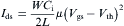
The inset of Fig. 1(b) shows the cross-sectional SEM images of the phosphorus (P)-doped nanogranular SiO2 films on Si substrate. Clear nanocolumnar microstructures with aligned nanochannels are observed. The thickness of the nanogranular SiO2 films deposited at room temperature is estimated to be ∼650 nm. Such loose structure helps to the absorption of H2O molecules within the nanogranular SiO2 films and the protonic/electronic hybrid behaviors. Fig. 1(b) shows the specific capacitance of the nanogranular SiO2 films as a function of frequency in the range between 1.0 Hz and 1.0 MHz. It can be seen that the specific capacitance increases with decreasing frequency. The maximum specific capacitance of ∼6.3 μ F/cm2 is obtained at 1.0 Hz. Such big specific capacitance is due to the formation of electric-double-layer (EDL) at the interface. Fig. 1(c) shows the transfer characteristics (drain current, Ids vs gate voltage, Vgs) of the IZO TFT gated by P-doped nanogranular SiO2 films in saturation region with a constant Vds of 1.6 V in a bottom gate structure. A hysteresis loop of ∼0.3 V is observed by the forward and reverse scan, which is suggested to be related to the migration of protons within the nanogranular SiO2 films [19] and [22]. Current ON/OFF ratio, subthreshold swing (S.S.) and threshold voltage (Vth) are estimated to be ∼6 × 10⁷, 80 mV/decade and − 0.1 V, respectively. Field-effect mobility (μ ) is estimated by the following equation:

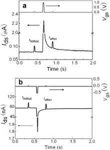
The modulation of the IZO channel conductance is related to the field-configurable protons flux within the nanogranular SiO2 films. The gate bias would trigger a transient protons flux within SiO2 films, therefore modulating the interplay between protons and electrons at the channel/dielectric interface. Due to the dynamic modulation of the migration of protons within the nanogranular SiO2 films by the gate bias, the channel current would be modified dynamically. Owing to such unique protonic/electronic hybrid properties, synaptic plasticity could be mimicked on the field-configurable nanogranular SiO2 gated IZO TFTs. The bottom gate could be deemed as the pre-synapse and the IZO channel with the source/drain electrodes could be deemed as the post-synapse. The IZO channel current was read out with a short read pulse on the gate before and after applying a gate input spike (programming pulse). Fig. 2(a) shows the IZO channel current as a function of time after applying a read pulse (0.05 V, 20 ms) and a single programming pulse of 1 V in amplitude and 30 ms in duration time. A constant Vds of 0.5 V was applied to the drain with the source grounded. The interval time between the read pulse and the programming pulse is 250 ms. Before applying the positive programming pulse, the initial drain current (Iinitial) is ∼102 nA by applying a read pulse on the gate. After applying the positive programming pulse, the drain current (Iafter) increases to ∼119 nA by applying a read pulse on the gate. Interestingly, for the negative programming pulse of − 0.5 V in amplitude and 30 ms in duration time, Iafter is lower than Iinitial (91 nA vs 97 nA), as shown in Fig. 2(b). When the pulse ends, the current gradually decays back to a static equilibrium state. The temporal profile of the current is comparable to those observed in biological synapses.
 | Fig. 2 IZO channel current as a function of time after applying a read pulse (0.05 V, 50 ms) and a single programming pulse with a constant Vds of 0.5 V: (a) A positive programming pulse of 1 V in amplitude and 30 ms in duration; (b) A negative programming pulse of − 0.5 V in amplitude and 30 ms in duration. |
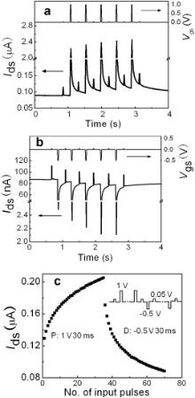
The transistors can also be dynamically programmed to arbitrary states by applying gate programming pulses with different amplitude and different polarity. A series of positive programming pulses with fixed amplitude of 1 V and fixed duration time of 30 ms were applied to the bottom gate. A constant Vds of 0.5 V was applied to the drain. After each programming pulse, the transistor was stabilized at Vgs = 0 V for 250 ms. Then the drain current was measured by applying a read pulse (0.05 V, 20 ms) on the gate. The interval time between two programming pulses is 500 ms. As shown in Fig. 3(a), the current read out by the read pulse progressively increases with the increase of the number of the positive programming pulses. A series of negative programming pulses with fixed amplitude of − 0.5 V and fixed duration time of 30 ms were also applied to the bottom gate. Different behaviors are observed. As shown in Fig. 3(b), the current read out by the read pulse progressively decreases by the negative programming pulses. The progressive increasing and decreasing in channel current as a function of constant programming pulse trains are similar to the response of synapse with facilitating process and depressing process, respectively [9]. The phenomena suggest that the drain current can be gradually adjusted by tuning the numbers and polarity of the programming pulses. Fig. 3(c) illustrates the drain current when the device is configured by a series of identical positive programming pulses (1 V, 30 ms) followed by a series of identical negative programming pulses (− 0.5 V, 30 ms). The drain current was measured at a small read pulse of 0.05 V on the gate with a constant Vds of 0.5 V after each programming pulse. The interval time between the read pulse and the programming pulse is 250 ms. The application of positive programming pulses (P) progressively increases the drain current, while the application of negative programming pulses (D) gradually decrease the drain current. Under the influence of an electric field, the continuous potentiation and depression contribute to modulating the drain current precisely. The increase (or decrease) in the drain current observed here is analogous to short-term synaptic potentiation (or depression) of synapses in biological systems.
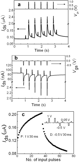 | Fig. 3 IZO transistors response to programming pulses. The channel current is read out by applying a read pulse (0.05 V, 50 ms) with a constant Vds of 0.5 V. (a) Current (lower curve) is progressively increased by applying a series of positive programming pulses with amplitude of 1 V (upper curve). (b) Current (lower curve) is progressively decreased by applying a series of negative programming pulses with amplitude of − 0.5 V (upper curve). (c) The channel current can be progressively increased or decreased by consecutive positive (P: 1 V, 30 ms) or negative (D: − 0.5 V, 30 ms) programming pulses. |
The operation mechanisms of the synaptic plasticity are discussed as follows. When a positive bias at the bottom gate electrode is applied, mobile protons (H+) within the P-doped nanogranular SiO2 films will move to the area near the interface of the top IZO channel and result in the formation of an interfacial electric-double-layer (EDL)[19]. On the one hand, protons (H+) dissociated from SiH4 and PH3 during the PECVD process will enter the nanogranular SiO2 films. On the other hand, the loose nanogranular SiO2 films exposed to the atmosphere would absorb H2O molecules within SiO2 films, in which hydrogen bonds with the hydroxyl groups[23] and [24]. When a positive gate programming pulse arrives, a transient proton flux is triggered within the nanogranular SiO2 films. Then the protons (H+) will accumulate at the SiO2/IZO channel interface, resulting in the accumulation of electrons in the IZO channel. With the increase of the numbers of the positive gate programming pulse, the phenomena of potentiation are observed. When a negative gate programming pulse arrives, a transient proton flux with opposite direction is triggered within the nanogranular SiO2 films. Therefore the electron in the IZO channel can be depleted. With the increase of the numbers of the negative gate programming pulse, the phenomena of depression are observed. The microporous structure of the nanogranular SiO2 films plays an important role in field-configurable operation. The short-term synaptic plasticity mimicked on the proposed IZO synaptic transistors is related to the dynamic modulation of the protons flux within the SiO2 nanogranular films.
In summary, an indium-zinc-oxide based ionic/electronic hybrid synaptic transistor gated by field-configurable nanogranular SiO2 films was demonstrated. High electrical performances are illustrated, such as a high drain current ON/OFF ratio of above 107, a low subthreshold swing of 80 mV/decade and a high electron mobility of 14 cm2 V− 1 s− 1. Due to the dynamic modulation of the transient protons flux within the nanogranular SiO2 films, the channel current would be modified dynamically. Short-term synaptic plasticities, such as short-term potentiation and short-term depression, were mimicked on the proposed IZO synaptic transistor. The synaptic transistor proposed here has potential applications in future neuromorphic devices.
The authors have declared that no competing interests exist.
| [1] |
|
| [2] |
|
| [3] |
|
| [4] |
|
| [5] |
|
| [6] |
|
| [7] |
|
| [8] |
|
| [9] |
|
| [10] |
|
| [11] |
|
| [12] |
|
| [13] |
|
| [14] |
|
| [15] |
|
| [16] |
|
| [17] |
|
| [18] |
|
| [19] |
|
| [20] |
|
| [21] |
|
| [22] |
|
| [23] |
|
| [24] |
|