Characterisation of Photocathodes Based on Pb Thin Film Deposited by UV Pulsed Laser Ablation
1. Istituto Nazionale di Fisica Nucleare e Università del Salento, Lecce, Italy
2. Università del Salento, Dipartimento di Matematica e Fisica “E. De Giorgi”, Lecce, Italy
3. Laboratori Nazionali di Frascati, Istituto Nazionale di Fisica Nucleare, Frascati, Italy
4. Center for Biomolecular Nanotechnologies, Istituto Italiano di Tecnologia, Arnesano, Lecce, Italy
5. Dipartimento di Ingegneria dell'Innovazione, Università del Salento, Lecce, Italy
6. National Nanotechnology Laboratory (NNL), CNR – Istituto Nanoscienze, Lecce, Italy
Corresponding author. Ph.D.; Tel.: +39 832 297501.
1. IntroductionRecently, metallic photocathodes have attracted much research attention with respect to the competitive photocathodes based on semiconductors. Although generally, the latter guarantee higher emission efficiencies, metallic photocathodes have several advantages, such as longer lifetime, shorter response photoemission time and high robustness [1], [2], [3] and [4]. Many groups have investigated the performance of metallic photocathodes under different operational conditions with the aim of improving their relatively low quantum efficiency (QE). The results of these investigations indicate that yttrium and magnesium are the most promising metallic photocathodes [5], [6], [7], [8] and [9]. Such materials provide better photoemission performance with respect to Cu, which is currently the most used metallic photocathode in the conventional radio frequency photoinjector guns, despite having a QE that is not very high (1.4 × 10⁻⁴ @ 266 nm).
For free electron laser development, it is necessary to obtain electron beams with significant average currents (>1 mA). Superconducting radio frequency guns (SRF-guns) are more recent and competitive potential solution because they are able to operate with continuous wave (cw) and near-cw sources at high accelerating gradients (>20 MV/m) and with lower dissipated power [10] and [11] with respect to conventional photoinjector guns.
Despite these advantages, the principal drawback of SRF-guns is the low QE of superconductors, mainly Nb, which is the most commonly used photocathode for such cavities [12] and [13]. This drawback can be overcome by incorporating a photocathode made of an alternative material with higher photoemission performance [10], [11], [12] and [13]. The challenge faced when trying to incorporate a different photocathode into an SRF-gun is to preserve both the quality factor of the superconducting cavity and the QE of the alternative photocathode material [14]. A smart solution seems to be the use of a photocathode based on Pb thin film. First, the superconducting temperature of Pb is quite similar to that of Nb; second, the QE of Pb bulk (around 7 × 10⁻⁵ @ 250 nm) [15] is much higher than that of Nb bulk (around 1 × 10⁻⁵ @ 250 nm) [15]; in addition, other important reasons are its higher chemical stability and the possibility to preserve the superconducting properties of Nb cavities [14].
Currently, the feasibility of Pb photocathodes has been tested for both bulk materials and thin films. Different deposition techniques have been used for the realisation of Pb thin films, such as electroplated deposition, arc deposition, sputtering and evaporation [11] and [16] but very little work has been done with pulsed laser ablation deposition (PLAD). The deposition of Pb thin films by PLAD was investigated in our previous work by using the fundamental wavelength of an Nd:YAG laser operating in the near-IR region (1064 nm) [17]. The deposited films were polycrystalline with high droplet density on the film surface. Moreover, the films were non-homogeneous, whereas grain dimensions increased with the laser fluence. Because of the restrictive needs of photocathodes in SRF-guns, the quality of Pb films must be improved further in terms of reduced droplet density and higher uniformity.
It is well known that the morphological features of thin films obtained by PLAD are strictly related to the choice of the laser parameters, such as laser wavelength. Therefore, in this work, PLAD deposition by UV laser beam was performed with the aim of obtaining a photocathode based on Pb thin film with an improved structure making possible the study of the photoemission properties of such device.
2. ExperimentalThe target ablation was performed by the fourth harmonic of an Nd:YAG laser (266 nm, Continuum Powerlite-8010, τ = 7 ns, f = 10 Hz) in a high vacuum system [18]. The operating laser fluence was fixed at 0.5 J/cm2 by using an energy attenuator; the value of laser fluence was chosen to be very close to the laser ablation threshold, Fthr ≈ 0.4 J/cm2, which was calculated theoretically according to the thermal model of Singh and Narayan [19], in order to reduce as much as possible the ejection of melt material from the target surface [20].
The laser beam was guided on the Pb target surface (99.9% purity) by using a mirror and a focused lens, leading to a laser spot size on the target surface of about 1.4 mm. The laser beam was incident on the target surface at an angle of 45°; Si (100) or Nb substrate was placed in front and parallel to the target at a distance of 5 cm. The target was rotated to avoid both the formation of deep craters and the plume deflection effect [21]. The Si (100) substrates were used as-received without any additional surface polishing treatment, while the Nb substrates were mechanically polished before the deposition. However, both kinds of substrates were cleaned with electronic grade acetone and ethanol. The Pb films were grown at room temperature with a base pressure of 10-5 Pa. The quality of the vacuum was supervised by a quadrupole mass spectrometer (Hiden Analytical HALO 201 RC). The partial pressures of oxygen (1 × 10⁻⁷ Pa) and water (5 × 10⁻⁷ Pa) were low enough to ensure high quality films in terms of chemical purity.
For each film deposition, 20,000 laser pulses were applied, which corresponded to 650 pulses/site. The number of pulses per site was calculated by multiplying the total number of shots, by the ratio of the laser spot area, to the area of the circular target track. The average ablation rate was 0.27 ± 0.02 μg/pulse, deduced by weighing the target before and after the ablation process. The etching rate of the target surface was of 16 nm/pulse.
The film morphology was studied by scanning electron microscopy (SEM, model JEOL-JSM-6480LV) and atomic force microscopy (AFM, Nanoscope III controller with Digital Instruments Multimode head, integrated with J-scanner) in tapping mode.
The structure and crystal orientation of the material was studied by X-ray diffraction (XRD) measurements performed on as-deposited samples in the Bragg–Brentano geometry using a Rigaku D/MAX-Ultima diffractometer equipped with a MPA2000 thin film attachment stage and a Cu anode.
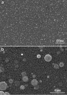
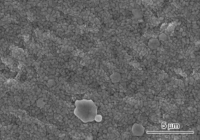
3. Results and Discussion Fig. 1 shows the morphological structure of the Pb film deposited on Si (100) substrate. A very large droplet density can be clearly observed at low magnification ( Fig. 1(a)); in fact, the film surface seems to be completely covered by droplets of different sizes and with a higher density than that found in our previous work using a laser wavelength of 1064 nm [17]. Moreover, the SEM image of the film at high magnification ( Fig. 1(b)) reveals a granular structure with a large presence of voids not allowing the formation of a continuous film. In addition, this granular structure is also replicated on the surface droplets, which are not completely spherical, as can be clearly seen in Fig. 1(b). This fact could be attributed to a large surface tension, which leads to the growth of the film on the substrate surface as an agglomeration of grains in the micrometric range.
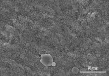
When Pb is deposited on the Nb substrate ( Fig. 2), the coverage of the substrate is better, avoiding the appearance of significant voids even though the film structure remains granular. Because of the experimental conditions, the ablation process was the same for all the experiments. The differences found in the film grown on different substrates could be attributed to the mechanism involved directly in the growth process of the Pb film over the substrate surface, where the competition between surface tension and nucleation will determine the final structure of the film. In those cases where the surface tension is greater, the substrate surface is not completely covered, whilst in the opposite cases the granular film covers nearly completely the substrate. This last structure seems to be more favourable for the realisation of photocathodes based on Pb thin films with PLAD technique.
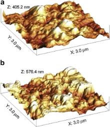
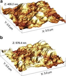
Fig. 3 reports the AFM inspection of the sample deposited on Si (100) and Nb substrates. The μ-scale morphologic structure of the Pb film can be clearly appreciated on the three-dimensional (3D) view AFM image, corroborating the results obtained by SEM. Fig. 3(a) and (b) shows an irregular granulometric distribution of Pb with a root-mean square roughness of about 58 and 108 nm and a maximum grain height of about 400 nm and 580 nm for Si and Nb, respectively. While a higher roughness is expected for the Pb film deposited on silicon, due to the stronger surface tension, the film deposited on the Nb substrate presents the highest surface roughness. Such behaviour can be most likely ascribed to the roughness of the Nb substrate. Even though the substrate was mechanically polished before the deposition, the roughness of Nb is much higher than that of Si (100), which has a very smooth morphology.
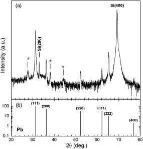
Fig. 4(a) shows the XRD pattern of a Pb film deposited on Si (100). In addition to the (200) and (400) peaks of the Si substrate, the figure shows a relatively intense peak at an angle of 31.30°, along with weaker peaks at 36.26°, 52.24°, 62.14°, 65.24° and 76.95° ascribed to the Pb deposit in the cubic crystalline form. The peaks can be ascribed to the (111), (200), (220), (311), (222) and (400) peaks of cubic Pb, respectively. Moreover, a comparison with the polycrystalline (powder) XRD pattern of Pb in Fig. 4(b) indicates that the (111) diffraction peak measured for the as-deposited metal film is relatively more intense than that expected for a randomly oriented polycrystalline sample, demonstrating that Pb deposition onto the substrate occurs preferentially along the (111) planes.
A few additional weak diffraction peaks at 27.68°, 38.12° and 44.04°, indicated with an asterisk (*) in Fig. 4(a), could be tentatively ascribed to the formation of lead silicates (most likely PbSiO3) [22] and [23]. The occurrence of these peaks suggests that energetic Pb atoms and ions during PLAD may interact with the native oxide layer on the Si substrate surface and residual (vacuum background) oxygen in the chamber to form lead silicate crystallites.
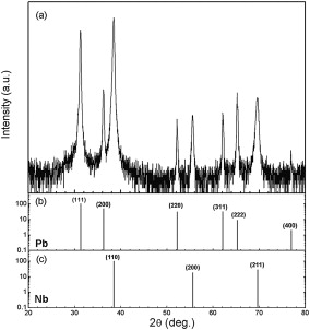
For the Pb film deposited on Nb ( Fig. 5), it is also possible to observe the same peaks ascribed to (111), (200), (220), (311), (222) and (400) crystalline planes of cubic Pb. Also, in this case, the Pb deposit appears preferentially oriented along the (111) planes. This fact proves the polycrystalline character of the films deposited on both substrates, as well as their common preferential orientation.
It is noteworthy to observe that in this latter case, no peaks corresponding to lead silicates were detected in the pattern, supporting our previous hypothesis that lead silicates could form on Si substrate upon reaction of Pb with the native silicon oxide surface.
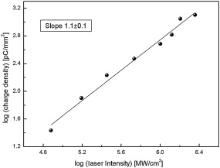
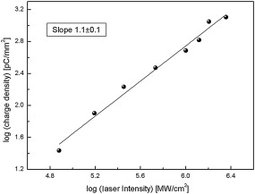
Studies on the photoemission performance of Pb thin films deposited on Nb substrate have been carried out in a photodiode cell [24]. The QE was in average 6 × 10⁻⁵ at a laser-driven photoemission of a wavelength of 266 nm, calculated as the ratio between the number of photoemitted electrons and the number of photons that impinge the cathode surface with the hypothesis of a single-photon emission. The data of the photoemitted charge as a function of laser energy ( Fig. 6) have been managed according to the generalised Fowler–Dubridge equation, J = CI n, where J is the current density, C is a constant, I the laser intensity and n the number of photons that are absorbed per electron emitted, in order to demonstrate that the photoemission is induced mainly by single-photon absorption [25]. The dependence of the charge density on I n in a log–log scale provides an easy method to examine the dominant process in the photoelectron emission. The data plot (dot points) of Fig. 6 shows a linear fit (continuous line) with a slope of 1.1 ± 0.1, which indicates that a single-photon absorption is the main photoemission process.
These interesting results demonstrate the low chemical reactivity of Pb to the gas environment; contrarily, for photocathodes based on Mg thin films deposited by PLAD, the formation of contaminant compounds on its surface, due to the air exposure, is responsible for photoemission processes induced by multi-photon absorption [8]. In that case laser cleaning of the cathode surface is mandatory to improve the photoemission performances of the cathode device.
4. ConclusionPLAD carried out by UV laser beams has been successfully proposed as a deposition technique for the realisation of Pb thin films adhered to substrates for the realisation of useful photocathodes in SRF-guns. The films deposited with 266 nm were more homogeneous and presented a bigger grain size than the films obtained with a wavelength of 1064 nm. It has also been observed that the morphological features of the films were improved on the Nb substrate, showing the growth of granular but uniform Pb thin film covering completely the substrate. XRD patterns revealed the growth of polycrystalline Pb film, regardless of the substrate, with a preferential orientation along the (111) planes. Photoemission testing of a photocathode based on Pb thin film showed a single-photoemission process with an average QE of about 6 × 10⁻⁵ @ 266 nm. Moreover, we believe that further work could be done in order to obtain photocathodes based on Pb thin films with better morphology, as this is responsible for the enhancement of the photoemission performance of Pb cathodes, improving not only the QE but also the emittance of the photoemitted electron beams.
Acknowledgements AcknowledgementThis work was supported by the Italian National Institute of Nuclear Physics (INFN).
The authors have declared that no competing interests exist.


 , Lorusso Antonella