

1. Introduction
Negative permittivity (epsilon-negative, ε′ < 0) is common in metals below their plasma frequency due to the plasmonic state of free electrons [1,2]. Negative dielectric properties of metals have shed light on the investigation and construction of metamaterials, while the tailorable negative permittivity in metamaterials depends on the geometric dimensions and configurations of metal building blocks [[3], [4], [5]]. Negative permittivity and negative permeability, also called double negative parameters of metamaterials, provide fresh options for wave absorbers and other electromagnetic applications [6,7]. In past several years, numerous studies demonstrated that negative permittivity can be also realized in composites with functional metal fillers randomly dispersed in insulator matrix [[8], [9], [10]]. In such materials, the realization and tunability of negative permittivity depends on the distribution and existing state of conductor fillers within the composites. The formed percolation conducting networks inside the insulating matrix permit delocalized electrons move macroscopically, leading to the state of plasma oscillation under external electric field and as a result negative permittivity appears [11,12]. Negative permittivity composites have shown great potential in various applications, such as electromagnetic shielding and wave-absorbing, novel multilayered capacitance, and coil-less electrical inductor’s design [[13], [14], [15], [16]]. Compared with metamaterials, composites take advantages on that the complicated artificial structures can be avoided but the designability of negative permittivity property can be still guaranteed. However, the anomalous dielectric behaviors in both metamaterials and composites are always based on the self-properties of building blocks or metallic fillers.
In fact, negative permittivity property hinges on the nature of carriers in material. Extremely high electron concentration of metals leads to that their plasma frequency usually distributes in ultraviolet band. And the classical free electron theory suggests that gigantic negative permittivity decreases rapidly as frequency decreases to the range far below metal’s plasma frequency [17,18]. Metamaterials and composites can be regarded as diluted metals to realize tailorable negative permittivity properties by controlling the average electrons concentration [19,20]. Furthermore, negative permittivity can be tuned by means of exerting external effect due to that electrons existing and transporting state is sensitive to the action of field like electric and temperature [[21], [22], [23]]. From the perspective of relationships between negative permittivity and electrons, it’s credible and significant to realize desirable negative dielectric performances in homogeneous materials of pure phase. In Yan’s work, Sr-doped LaMnO3 was synthesized and of which the plasma-like negative permittivity behaviors were dominated by Sr-dopants amount that determined effective electrons concentration [24,25]. Moreover, the variable carrier concentration of single-phase materials like doped semiconductors under external field actions helps to achieve tailorable negative dielectric properties [26]. Tunable negative permittivity realized in mono-component materials is full of enlightening significance to elucidate the mechanism through investigating material’s intrinsic parameters of carrier concentration and mobility. Moreover, compared with composites, mono-phase materials are more liable to be films or coatings that could extend the application scenario of epsilon-negative materials to two-dimensional or even smaller scale.
However, in most reports, negative permittivity was roughly attributed to the critical structures of building blocks both in metamaterials and composites, while investigations on the relationships between negative permittivity and carrier characters were rarely involved. In this work, tin-doped indium oxide (ITO) was sintered into mono-phase bulks to study the relevance between negative permittivity and carriers. It’s well known that ITO with appropriate doping ratio possesses excellent conductivity and has been widely studied for transparent conducting materials and electro-optical applications [27,28]. Meanwhile, the optical dielectric function and carrier concentration of ITO can be easily tailored through trimming dopants amount and preparation conditions [29,30]. In addition, carriers’ intrinsic characteristics in semiconductors can be easily and quantitatively studied by the aid of Hall effect. Therefore, ITO was sintered for epsilon-negative material in this work, where the generation and regulation mechanism of negative permittivity property were also investigated from a more microcosmic perspective.
2. Experimental
ITO was synthesized through solid state reactions of indium oxide (In2O3) uniformly mixed with 9 mol % tin oxide (SnO2). Samples with same composition were respectively sintered at 1300 °C for 180 min in oxygen (O2), air, and argon (Ar) atmosphere to investigate the influences of different carrier concentration caused by sintering conditions on negative permittivity properties.
Phase and chemical compositions were characterized with X-ray diffraction (XRD, Dmax-2500PC, Rigaku) and X-ray photoelectron spectrometer (XPS, Axis Supra, Shimadzu). Morphologies and microstructures were observed with field emission scanning electron microscope (FE-SEM, SU-70, Hitachi). Ac conductivity (σac) and complex permittivity (ε = ε′ - iε′′) spectra were measured with impedance analyzer (E4991A, Agilent) equipped with 16453A dielectric test fixture from 10 MHz to 1 GHz. Temperature-dependent dielectric properties at kHz frequencies were measured with LCR meter (E4980AL, Keysight) fitted with a self-built temperature-varying system from 20 °C to 650 °C. Carrier concentration and mobility of ITO bulks were measured by hall effect test system (Model HALL series, Semishare) with Van der Pauw method [31]. Samples for Hall test are 1 cm2 thin slices with thickness of 0.5 mm. Induction strength of the applied magnetic field was 0.3 T and the excitation current was 5 mA.
3. Results and discussion
3.1. Composition and microstructure
Fig. 1 shows the XRD patterns of ITO ceramics sintered in different atmosphere. It’s apparent that all samples possess high crystallinity and hold the main crystal phase of cubic In2O3 (PDF#71-2194). Tetragonal SnO2 (PDF#77-0447) diffraction peaks appeared on the pattern of ITO sintered in O2 but become invisible in Air and Ar. This was caused by the different solid solubility of SnO2 into In2O3 during sintering in the varied atmosphere. It seems that oxygen insufficiency of sintering atmosphere promotes the doping process for Sn atoms into In2O3 crystal lattice. As a result, ceramics sintered in Ar have the largest solubility for SnO2 incorporating into In2O3, leading to the vanishing diffraction peaks of tetragonal SnO2. This also indicated that there may be more effective Sn-dopants for ITO sintered in oxygen-deficient atmosphere. In addition, details of the main diffraction peaks near 2θ = 30.6° are shown in Fig. 1(b). On the standard pattern of undoped In2O3, diffraction peak of (222) crystal planes appears at 2θ = 30.585°. However, it shifted obviously towards high angle on patterns of doped samples, regardless the sintering atmosphere. In fact, interplanar spacing decreased as Sn atoms with smaller atomic radius substitutionally doped into the crystal lattice. According to Bragg’s equation (2dsinθ = nλ), it’s reasonable that diffraction peaks shifted to high angle as interplanar spacing decreased [32]. This also proved the successful doping of Sn atoms.
Fig. 1.
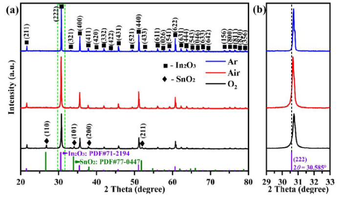
Fig. 1.
XRD patterns of ITO ceramics sintered in O2, Air, and Ar, respectively. (b) Details of diffraction peaks of (222) crystal plane.
To further verify the composition, chemical valence states of the constituent elements in ITO were analyzed with XPS [33]. Survey spectra in Fig. 2(a) show Sn, O, and In elements exhibits strong photoelectron spectra peaks, symbolizing electron chemical states of different orbits. Fine spectra of Sn3d5/2, O1s, and In3d5/2 were deconvoluted to investigate elements specific existing states. Fig. 2(b) gives the results of Sn3d5/2 of ITO sintered in different conditions. Sn3d5/2 spectra were split into two peaks of Sn3d5/2 (I) and Sn3d5/2 (II). Sn3d5/2 (I) of higher binding energy corresponds with +4 oxidation state of Sn in SnO2 or the dissolved Sn element in In2O3 lattice, while Sn3d5/2 (II) of lower binding energy is corresponding to the tiny non-stoichiometric SnO2-x caused by oxygen-deficiency. Similarly, as shown in Fig. 2(c), O1s spectra were split into O1s (I) with higher binding energy and O1s (II) with lower binding energy. The higher binding energy of O1s (I) may be caused by the adsorbed oxygen, including oxygen atoms captured by oxygen vacancies, or oxygen molecules enchained by Sn atoms [34]. Note that the contribution of O1s (I) increased with the sintering atmosphere successively changed from O2 to Air and Ar. Therefore, the role played by oxygen vacancies in ITO electric or dielectric properties can never be ignored. Fig. 2(d) presents the analysis results of In3d5/2 fine spectra and there’s no obvious difference with the varied sintering atmosphere. In3d5/2(I) with higher binding energy is related to In3+ of normal valence state, while In3d5/2(II) with lower binding energy may arise from the tiny bit of In(3-x)+ in In2O3 crystal lattice.
Fig. 2.

Fig. 2.
XPS spectra of ITO ceramics: (a) survey spectra, (b) Sn3d5/2, (c) O1s, and (d) In3d5/2 fine spectra of samples sintered in O2, Air, and Ar, respectively.
From the perspective of defect reactions, the process of Sn-doping and the generation of oxygen vacancies can be described as following.
Doped Sn atoms substituted In atoms in crystal lattice and served as donors to provide n-type carriers (i.e., electrons). Oxygen vacancies with two charges emerged as O atoms escaped from the crystal lattice. Oxygen molecules (O2) generated in both the two processes abovementioned (1 and 2). It’s noteworthy that the generated O2 on right part of the reaction equations affected the dynamics of doping and defects generation. For reaction (2), the equilibrium constant $\text{K}=[\text{V}{{_{\text{O}}^{{}}}^{\cdot \cdot }}]{{[{{\text{p}}_{{{\text{O}}_{2}}}}]}^{1/2}}{{[{e}']}^{2}}/[\text{O}{{_{\text{O}}^{{}}}^{\text{x}}}]$ is sensitive to oxygen partial pressure of the sintering atmosphere and the condition of oxygen deficiency is favorable for the forward reaction. Meanwhile, the vacancies generated in (2) can promote (1) reaction due to lattice defects help to accelerate the mass transfer process of solid solutions. Therefore, defect reactions during sintering were influenced by the oxygen partial pressure of sintering atmosphere. Based on the above discussion, it’s reasonable that tetragonal SnO2 diffraction peaks vanished on XRD patterns of the ceramics sintered in Air and Ar due to the more complete solution under low oxygen partial pressure. Then, the varied microstructures and physical properties affected by defect reactions were further discussed in following sections.
Fig. 3 shows the SEM images of microstructure for ITO sintered in O2, Air, and Ar, respectively. Fractures of samples sintered in O2 and Air exhibit entirely intergranular behaviors, as shown in Fig. 3(a, b), while that for sample sintered in Ar was transgranular (as shown in Fig. S1). Hence, fracture surface of ITO sintered in Ar was heat eroded before SEM observation to get more grain details, and the microstructures are clearly shown in Fig. 3(c). For all samples, the grain boundaries are clear without any inclusions and grains of ITO contact closely to form dense ceramics. Furthermore, grain size increased with the decreasing oxygen partial pressure of sintering atmosphere, as demonstrated by the figures of grain size distribution in (d-f). This was caused by that defect reactions and the resultant vacancy defects also accelerated the mass transfer during sintering, contributing to grain boundary movement and grain growth. The dynamics was more favorable to grain growth when the sintering atmosphere was oxygen-deficient and the result was apparent that ITO sintered in Ar possessed the largest grain size. Besides, the amount of grain boundaries in per unit volume decreased with grain size increasing for the negative correlations between them.
Fig. 3.

Fig. 3.
Secondary electron images and grain size distribution of ITO ceramics sintered in O2 (a, d), Air (b, e), and Ar (c,f), respectively. (a) and (b) show the fresh fracture surface, (c) shows the fracture surface after heat erosion.
3.2. Carrier and electric conductivity
Fig. 4(a) shows the measured carrier concentration (n), mobility (μ), and calculated resistivity (ρ-1 = nμe) for ITO ceramics sintered in different atmosphere. Combined with the abovementioned results of XRD, XPS, and SEM, it’s interpretable that carrier concentration increased with the sintering atmosphere changing from O2 to Air and Ar because more Sn atoms dissolved into In2O3 lattice as donors to provide n-type carriers. Meanwhile, carrier mobility is determined by various scattering effects, including those caused by lattice vibration and lattice defects, as well as phase or grain boundaries [35]. Influences of phonon scattering on the different mobility of the three samples were not considered due to the current discussion was based on the same test temperature. Meanwhile, the mobility is also affected by impurity scattering effect but only at very low temperature is the mobility dominated by the scattering of ionized impurity centers. In addition, for sample sintered in O2 atmosphere, there existed residual SnO2 which is insulating and remained as the second phase in ceramic, and thus the mobility is also affected by the phase boundaries. Furthermore, grain boundaries of the polycrystalline ceramics are considered to be interfacial defects which have great influences on the transport and transfer of carriers. Therefore, the decreased amount of grain boundaries is favorable for carrier mobility increasing. Affected by the above factors, sample sintered in O2 atmospheres has the lowest mobility and sample sintered in Ar atmospheres has the highest mobility. As a result, resistivity of ITO ceramics decreased with the sintering atmosphere successively changing from O2 to air and Ar.
Fig. 4.

Fig. 4.
(a) Resistivity, carrier concentration and hall mobility of ITO ceramics sintered in different atmosphere. (b) Frequency dependence of σac for ITO ceramics sintered in different atmosphere.
Fig. 4(b) shows frequency dependence of ac conductivity (σac) for ITO ceramics sintered in different atmosphere. In high frequency electric field, carriers’ movement is always influenced by external field and the crystal lattice itself, and meanwhile σac is also closely related to carrier concentration and mobility. It can be seen that σac of ITO is sensitive to sintering atmosphere and oxygen-deficient conditions lead to larger conductivity. Considering the combined contributions of delocalized free electrons, as well as the charges localized by oxygen vacancies and other defects, the Drude-Lorentz oscillator model was used to account for the high frequency conduction behaviors, as described below [36].
The front part of the equation describes the contribution of free electrons to conductivity, while the end describes the resonance response of localized charges. σdc is the dc limit of Drude conductivity, τ is the average scattering time of carriers, ωpl is the Lorentz angular plasma frequency, ω0 is the resonance frequency, and γ is the damping factor. Solid lines in Fig. 4(b) are fitted results of Eq. (3) and agree well with the measured data. Actually, electrons provided by substitutional Sn4+ donors were delocalized in the ceramics to form currents under the action of electric field, while the localized charges, including those bounded by oxygen vacancies or localized by grain and phase boundaries, can’t move in large scale, showing a localized response like polarization. Therefore, Sn doping plays the dominant role in semiconducting ITO, and oceans of delocalized n-type carriers conduct like free electron gas depicted in the classical Drude theory. Furthermore, it’s noteworthy that the variation of σac with different sintering atmosphere is consistent with that of resistivity drawn from Hall measured data, indicating that it’s feasible to investigate the high frequency performances of ITO from the carrier characteristics.
3.3. Negative dielectric permittivity
Permittivity spectra were analyzed to investigate the dielectric properties of ITO in radio frequency range. Fig. 5(a) shows the frequency dependence of permittivity for ITO sintered in different atmosphere. Negative permittivity was realized in the whole measured frequency band. Variation tendencies of permittivity on frequency for the three samples are similar but the magnitudes of negative values are disparate with varied sintering atmosphere. The analyses and discussions abovementioned suggested that free carriers and localized charges both responded to external electric fields. Localized charges would orientate or become polarized, and free electrons would oscillate repeatedly on the direction parallel to electric field. So the Drude-Lorentz model was used to study the dielectric properties of ITO ceramics, the real part of complex permittivity (ε′) was described as following [37,38].
Fig. 5.

Fig. 5.
Frequency dependences of ε′ (a) and ε′′ (b) for ITO ceramics sintered in different atmosphere. Solid lines in (a) are fitted results of Drude-Lorentz model, and lines in (b) are fitted results of conduction loss.
Solids lines in Fig. 5(a) are fitted results of Eq. (4). The realized negative permittivity properties of ITO here are similar to metal’s plasmonic behavior below plasma frequency. There seems no apparent resonance characteristic for both the experimental data and fitting results. This is attributed to that resonance responses of localized charges were overwhelmed by the plasma oscillations of extensive electrons [21]. Therefore, the Drude mechanism plays the dominant role in realizing negative permittivity for ITO ceramics. According to Eqs. (4) and (5), frequency dispersion and magnitude of negative permittivity are closely related to carrier concentration. And as a result, it’s actually that ITO sintered in oxygen-deficient atmosphere possessed higher carrier concentration and larger values of negative permittivity.
The imaginary part of complex permittivity (ε′′) represents energy loss of the material in electric field. The exerted electric field would induce delocalized carriers migrate directionally to create electric currents, leading to that ε′′ of ITO was dominated by conduction loss [40,41]. ε′′ caused by conduction loss is usually inversely proportional to frequency, as ε′′∝ω-1 [42]. As shown in Fig. 5(b), the measured data of ε′′ were basically in agreement with the fitting results of conduction loss. Meanwhile, the polarization process of localized charges at grain or phase boundaries and defects also contributed to the total dielectric loss [43,44]. In addition, ε′′ was also sensitive to sintering atmosphere. ITO with higher carrier concentration hold larger dielectric loss. Specifically, for this case, the increased carrier concentration and the decreased resistivity enabled more conduction currents to be generated, resulting in the increased conduction loss.
Furthermore, the dielectric properties in kHz frequency band for ITO ceramics sintered in air were measured as temperature increased from 20 °C to 650 °C in air atmosphere. As shown in Fig. 6, frequency dependences of ε′ showed similar dispersion spectra like those at MHz frequencies, indicating the mechanism of plasma-like negative permittivity behavior was dominated by the extremely low frequency plasmonic state of free electrons [3,21]. Meanwhile, the magnitude of negative permittivity decreased with temperature increasing, and the dielectric loss which was dominated by conduction loss also decreased as temperature gone up. In addition, σac in kHz frequency region was evidently affected by temperature, while the decreasing tendency of σacversus to frequency indicated the conductivity is mainly contributed by free electrons. Conductivity of electrons in typical conductors is closely associated with electrons concentration (n), scattering time (τ), and effective mass (m*), as described below [24,45].
Fig. 6.

Fig. 6.
Temperature-dependent permittivity (a, b) and conductivity (c, d) spectra in kHz frequency region.
Free electrons move faster and more randomly as temperature increases, and the effect of phonon scattering is more significant at high temperature, leading to electron collisions more violent and the average free time (τ) decreasing [35]. Therefore, σac became smaller when temperature increased, and the variation of conductivity versus temperature (T) followed a relationship which is valid in typical metallic conductors, as follows [46,47].
where σT0 is conductivity of the material at a given temperature T0, α is the thermal expansion coefficient of the material. The measured conductivity data agreed well with this equation, as shown in Fig. 6(d), suggesting the conduction mechanism of ITO was similar with that in metallic conductors. At high temperature, carriers motion can’t be accelerated by the exerted electric field as effectively as at low temperature. Thus, plasma oscillation state of free electrons was affected and the resultant negative permittivity behaviors showed temperature-dependent performances. Moreover, the decreased ε′′ with increasing temperature further proved that dielectric loss of the epsilon-negative ceramics was mainly dominated by conduction loss.
4. Conclusion
In summary, Sn-doped ceramics of indium oxide were successfully sintered for epsilon-negative materials. Sn-doping was affected by the sintering condition and the resultant carrier concentration was influenced by the oxygen partial pressure of sintering atmosphere. Oxygen-deficiency was favorable for more Sn-atoms doping into In2O3 lattice as donors, resulting in increasing carrier concentration. Delocalized free carriers and localized charges at various defects both responded in electric field, while the negative permittivity behavior was mainly induced by the low frequency plasmonic state of free carriers. Magnitude and frequency dispersion of negative permittivity was dependent on free carriers’ collective responses and the dielectric loss was mainly dominated by conduction loss. Negative permittivity of mono-phase ceramics is the intrinsic property which is related to material’s nature. This work ascertained the mechanism of negative permittivity properties at MHz-kHz frequencies for doped ceramics preliminarily.
Acknowledgements
This work was supported by the National Natural Science Foundation of China (Nos. 51771104, 51871146, 51971119), the Future Plan for Young Talent of Shandong University (No. 2016WLJH40), and the Innovation Program of Shanghai Municipal Education Commission (No. 2019-01-07-00-10-E00053).
Appendix A. Supplementary data
Supplementary material related to this article can be found, in the online version, at doi:https://doi.org/10.1016/j.jmst.2020.06.013.
Reference
DOI URL PMID [Cited within: 2]
DOI
URL
PMID
[Cited within: 1]

We demonstrate a composite medium, based on a periodic array of interspaced conducting nonmagnetic split ring resonators and continuous wires, that exhibits a frequency region in the microwave regime with simultaneously negative values of effective permeability &mgr;(eff)(omega) and permittivity varepsilon(eff)(omega). This structure forms a
DOI
URL
PMID
[Cited within: 1]
The advent of negative index materials has spawned extensive research into metamaterials over the past decade. Metamaterials are attractive not only for their exotic electromagnetic properties, but also their promise for applications. A particular branch-the metamaterial perfect absorber (MPA)-has garnered interest due to the fact that it can achieve unity absorptivity of electromagnetic waves. Since its first experimental demonstration in 2008, the MPA has progressed significantly with designs shown across the electromagnetic spectrum, from microwave to optical. In this Progress Report we give an overview of the field and discuss a selection of examples and related applications. The ability of the MPA to exhibit extreme performance flexibility will be discussed and the theory underlying their operation and limitations will be established. Insight is given into what we can expect from this rapidly expanding field and future challenges will be addressed.
DOI
URL
PMID
[Cited within: 1]
The mechanism of negative permittivity/permeability is still unclear in the random metamaterials, where the precise control of microstructure and electromagnetic properties is also a challenge due to its random characteristic. Here silver was introduced into porous SiO2 microsphere matrix by a self-assemble and template method to construct the random metamaterials. The distribution of silver was restricted among the interstices of SiO2 microspheres, which lead to the precise regulation of electrical percolation (from hoping to Drude-type conductivity) with increasing silver content. Negative permittivity came from the plasma-like behavior of silver network, and its value and frequency dispersion were further adjusted by Lorentz-type dielectric response. During this process, the frequency of epsilon-near-zero (ENZ) could be adjusted accordingly. Negative permeability was well explained by the magnetic response of eddy current in silver micronetwork. The calculation results indicated that negative permeability has a linear relation with omega (0.5), showing a relaxation-type spectrum, different from the
DOI URL PMID [Cited within: 1]
DOI
URL
PMID
[Cited within: 3]
Intrinsic metamaterials with negative- k that originated from random-structured materials have drawn increasing attention. Currently, intrinsic negative- k was mainly achieved in percolative composites by tailoring the compositions and microstructures. Herein, plasmalike negative- k was successfully achieved in multiwalled carbon nanotubes (MWCNT)/polyimide (PI) nanocomposites via applying external dc bias which exhibited excellent capability in conveniently and accurately adjusting negative- k. Mechanism analysis indicated that the localized charges at the interfaces between MWCNT and PI became delocalized after gaining energy from the dc bias, resulting in elevated concentration of delocalized charges, and hence the enhanced negative- k. Furthermore, it is surprising to observe that negative- k also appeared in multilayer nanocomposites consisting of alternating BaTiO3/PI and PI layers, in which there was no percolative conducting network. On the basis of systematic analysis, it is proposed that the unique nonpercolative negative- k resulted from the mutual competition between plasma oscillations of delocalized charges and polarizations of localized charges. Negative- k appeared once the polarizations were overwhelmed by plasma oscillations. This work demonstrated that applying dc bias is a promising way to achieve highly tailorable negative- k. Meanwhile, the observation of unique nonpercolative negative- k and the clarification of underlying mechanisms offer new insights into negative- k metamaterials, which will greatly facilitate the exploration of high-performance electromagnetic metamaterials.
DOI
URL
PMID
[Cited within: 1]
Metal oxides (MOs) are the most abundant materials in the Earth's crust and are ingredients in traditional ceramics. MO semiconductors are strikingly different from conventional inorganic semiconductors such as silicon and III-V compounds with respect to materials design concepts, electronic structure, charge transport mechanisms, defect states, thin-film processing and optoelectronic properties, thereby enabling both conventional and completely new functions. Recently, remarkable advances in MO semiconductors for electronics have been achieved, including the discovery and characterization of new transparent conducting oxides, realization of p-type along with traditional n-type MO semiconductors for transistors, p-n junctions and complementary circuits, formulations for printing MO electronics and, most importantly, commercialization of amorphous oxide semiconductors for flat panel displays. This Review surveys the uniqueness and universality of MOs versus other unconventional electronic materials in terms of materials chemistry and physics, electronic characteristics, thin-film fabrication strategies and selected applications in thin-film transistors, solar cells, diodes and memories.
DOI
URL
PMID
[Cited within: 1]
Lightweight absorption-dominated electromagnetic interference (EMI) shielding materials are more attractive than conventional reflection-dominated counterparts because they minimize the twice pollution of the reflected electromagnetic (EM) wave. Here, porous Ti2CT x MXene/poly(vinyl alcohol) composite foams constructed by few-layered Ti2CT x (f-Ti2CT x) MXene and poly(vinyl alcohol) (PVA) are fabricated via a facile freeze-drying method. As superior EMI shielding materials, their calculated specific shielding effectiveness reaches up to 5136 dB cm(2) g(-1) with an ultralow filler content of only 0.15 vol % and reflection effectiveness (SER) of less than 2 dB, representing the excellent absorption-dominated shielding performance. Contrast experiment reveals that the good impedance matching derived from the multiple porous structures, internal reflection, and polarization effect (dipole and interfacial polarization) plays a synergistic role in the improved absorption efficiency and superior EMI shielding performance. Consequently, this work provides a promising MXene-based EMI shielding candidate with lightweight and high strength features.

 WeChat