Search for articles:
Young Wook Noh, In Su Jin, Sang Hyun Park, Jae Woong Jung
Corresponding authors:
Received: 2019-10-21
Revised: 2019-11-16
Accepted: 2019-11-20
Online: 2020-04-01
Copyright: 2020 Editorial board of Journal of Materials Science & Technology Copyright reserved, Editorial board of Journal of Materials Science & Technology
More
Abstract
The interface engineering plays a key role in controlled optoelectronic properties of perovskite photovoltaic devices, and thus the electron transport layer (ETL) material with tailored optoelectronic properties remains a challenge for achieving high photovoltaic performance of planar perovskite solar cells (PSCs). Here, the fine and crystalline zirconium stanate (ZrSnO4) nanoparticles (NPs) was synthesized at low temperature, and its optoelectronic properties are systematically investigated. Benefiting from the favorable electronic structure of ZrSnO4 NPs for applications in ETL, efficient electron transport and extraction with suppressed charge recombination are achieved at the interface of perovskite layer. As a result, the optimized ZrSnO4 NPs synthesized at room-temperature deliver the optimized power conversion efficiency up to 16.76 % with acceptable stability. This work opens up a new class of ternary metal oxide for the use in ETL of the planar PSCs and should pave the way toward designing new interfacial materials for practical optoelectronic devices.
Keywords:
Organic-inorganic hybrid perovskite semiconductor is one of the most emerging photoactive materials for solar cells, which offers the promise of becoming inexpensive, flexible, large-scale photovoltaic technology [[1], [2], [3], [4], [5]]. In the past few years, the photovoltaic performance of perovskite solar cells (PSCs) have been enhanced by advancements in materials design and device engineering, and the fruit of effort has been realized by achieving the power conversion efficiency (PCE) up to 25 % in single-junction device [6]. Interface optimization is another key strategy to render the photovoltaic performance of PSCs, because the surface composition, crystal phase, and film morphology of the perovskite absorber are highly dependent on the underlying interface properties [[7], [8], [9]]. Moreover, the charge transport, extraction and recombination kinetics of PSCs are primarily governed by the electronic structure of the interface in the device. Up to now, the state-of-the-art PSCs are mostly fabricated in the mesoporous structure in which mesoporous titanium oxide (TiO2) is required as an electron transport layer (ETL) for efficient electron extraction with effective hole blocking from perovskite absorber layer. Unlike organic n-type semiconductors (e.g., fullerene and conjugated polymers) which are advantageous in simple and low-temperature processing with const-effectiveness, the TiO2 is a favorable ETL material due to its high optical transparency and excellent electron mobility [10]. However, the ideal mesoporous TiO2 usually formed through sintering process at >450 °C, and thus it is incompatible with low-cost fabrication and flexible substrate [11]. The planar heterojunction structure in which compact ETL of n-type metal oxides such as zinc oxide (ZnO), TiO2, or tin oxide (SnO2) layer has been demonstrated as an alternative to the mesoporous structure because of the potential in scalable and flexible device fabrication of PSCs. In specific, the colloidal nanoparticles (NPs) synthesized at low-temperature (room temperature (RT)-150 °C) are favorable for the compact ETL in the planar PSCs because the colloidal NPs are advantageous in controlling crystal structure, surface defects, and electronic properties [12]. Various types of colloidal NPs have been designed and synthesized, and high PCEs in the planar PSCs have been reported [[13], [14], [15]]. The n-type binary oxide semiconductors have been explored due to their analogy with TiO2, but most of those exhibited unsatisfactory device performances. On the other hand, ternary metal oxides (TMOs) are another interesting class of oxide semiconductors due to their potential for tunable optical and electronic properties [16,17]. In recent years, a few TMO such as Zn2SnO4 or NiCo2O4 has been reported for the use in PSCs as an interfacial layer exhibiting the controlled charge transport properties [[18], [19], [20], [21]]. Among them, Sn-based TMOs have been studied due to its excellent optoelectronic properties comparable to SnO2 coupled with potential transparency and chemical stability. Kim et al. reported the BaSnO3 NPs as a photoanode in dye-sensitized solar cells (DSSCs), which demonstrated PCE of 5.2 % [22]. La-doped BaSnO3 have also been used as mesoporous scaffolds in PSCs, and effective hole blocking was demonstrated [23]. Despite these works promise the potential of Sn-based TMOs as ETLs for PSC devices, the most of the TMO-based ETLs are prepared via high-temperature processing at present, which limit their further development in the low-cost production and their practical applications [24].
In an attempt to explore novel TMO-based ETLs for efficient PSCs, we herein demonstrate a successful synthesis of zirconia stanate (ZrSnO4) NPs at low-temperature and its application in planar PSCs as an ETL. The electronic structure and corresponding optoelectronic properties of ZrSnO4 NPs were optimized by varying the synthesis temperature, and the correlation between different ZrSnO4 NPs and the subsequent photovoltaic performance was systematically investigated. The optimized device based on ZrSnO4 NPs yielded promising PCE of 16.76 % with a VOC 1.00 V, a JSC 24.75 mA/cm2 and a fill factor (FF) of 0.67. Systematic analyses concluded that ZrSnO4 NPs render efficient electron extraction with suppressed charge recombination at the interface, which promises ZrSnO4 NPs as a low-temperature ETL material for efficient PSCs and other photoelectric devices.
The precursor solution of ZrSnO4, SnCl4 · 2H2O (10 mmol) and ZrCl2O·8H2O (10 mmol) were dissolved in hydrogen peroxide (34 ml), and then 192.2 mg of citric acid was added to the mixed solution with stirring. After 30 min, the ammonia solution was added to the mixture slowly to set the pH to 10, which induced the solution to be opaque (milky color). The solution was further stirred for 24 h with varied temperature (RT, 55 °C, and 75 °C). The heated samples (55 °C and 75 °C) were synthesized by continuous stirring in the heating mantle at a designated temperature, while the RT samples were stirred without any heat treatment. After the milky solution was washed with deionized water and ethanol twice, the decant of the dispersion was centrifuged, and the final product was dispersed in 2-methoxy ethanol to 0.5 wt%. The low band gap perovskite precursor solution was prepared as reported elsewhere [25]. The precursor solution of low band gap perovskite, 1.4 M of leadiodide, 0.07 M of methylammonium bromide, 1.4 M of formammoium iodide, and 0.07 M of leadbromide were dissolved in dimethylsulfoxide and dimethylformamide (1:8 in volume). After the solution was stirred at room temperature for 20 min, a precursor solution was filtered by PTFE-D filters with a pore size of 0.2 μm.
The ITO-coated glass substrates (20 Ω/sq) were cleaned sequentially with deionized water, acetone, and isopropanol under sonication for 15 min, and then the substrates were treated with UV-O3 for 30 min. After the ZrSnO4 nanoparticles layer was formed by spin-coating onto the ITO-coated glass (3000 RPM for 30 s), the substrate was annealed in ambient atmosphere for 1 h at 100 °C. After the substrates were cooled to RT, we treated UV-O3 for 15 min. And then the low band gap perovskite layer ((FAPbI3)0.95(MAPbBr3)0.05) was formed by spin-coating the precursor solution at 1000 rpm for 10 s and 3000 rpm for 20 s. After 14 s, 400 μL of ether was poured on top of the substrates during spin-coating. After thermal annealing at 150 °C for 3 min, the Spiro-OMeTAD (90.9 mg mL-1) in chlorobenzene with 39 μl 4-tert-butylpyridine (tBP) and 23 μl bis(trifluoromethane)sulfonamide lithium salt in acetonitrile (ACN) (540 mg mL-1) was deposited by dynamic spin-coating at 2000 rpm for 25 s. Finally, 80 nm of Au was evaporated under high vacuum (<5 × 10⁻⁶ Torr). The device area was defined by the shadow mask as 10 mm2.
Elemental investigation was carried out using X-ray photoelectron spectroscopy (K Alpha, Thermo Science). Ultraviolet photoelectron spectroscopy spectra were obtained by AXIS Ultra DLD (Kratos. Inc) equipped with He I source (hv =21.2 eV) at Korea Basic Science Institute. Absorption and transmittance measurements were carried out using a spectrometer (8453 , Agilent) at the Core Facility Center for Analysis of Optoelectronic Materials and Devices of Korea Basic Science Insittute (KBSI). The fluorescence of the sample was measured using a spectrofluorometer (FS5, Edinburgh instruments). The fluorescence lifetime of the sample was monitored by time-correlated single photon counting system using the picosecond laser with an excitation at 405 nm. Thin film morphology was observed using an atomic force microscope (CoreAFM, Nanosurf) in tapping mode and field-emission scanning electron microscopy (S-4800, Hitach). The photovoltaic performance of PSCs were obtained from parameter analyzer (4200-SCS, Keithley) under AM 1.5 G (100 mW cm-2) illumination, which was carefully calibrated using a NREL-certified photodiode. The external quantum efficiency (EQE) of the device was measured using lock-in amplifier system which records the short-circuit current density under chopped monochromatic light. Electrochemical impedance spectroscopy of the devices was investigated using a potentiostat (Compactstat, IVIUM). Intensity-modulated photovoltage spectroscopy (IMVS) and photocurrent spectroscopy (IMPS) were measured by potentiostat with a light emitting diode (LED) system (IVIUM, IM1225).
For synthesis of colloidal NPs of ZrSnO4, the precursor solution of ZrCl2 and SnCl2 were dissolved in DI water with hydrogen peroxide for hydrolysis. The citric acid was added in the solution as a directing agent of metal precursors during the hydrolysis because it can chelate metal ions with the carboxylate groups [26]. Subsequently, the precursor solution was treated with ammonia to induce dehydration and redox reaction for condensation process, where the ammonia molecules can also passivate the surface with accelerated stabilization of NPs in alcohol medium. As the nanoparticles are formed, the solution becomes opaque with a milky color, as shown in Fig. 1(a). The dehydration process for NP synthesis was controlled by varied temperature of the medium to further optimize ZrSnO4 NPs. The ZrSnO4 NPs were readily dispersed into 2-methloxyethanol with a solubility of >50 mg ml-1 regardless of the synthesis temperature, and the solutions were stable in the ambient environment without obvious precipitation regardless of synthesis temperature. (Fig. S1) The transmission electron miscropy (TEM) images for ZrSnO4 NPs synthesized at different temperatures are shown in Fig. 1(b-d). The TEM images confirm a uniform dispersity of the NPs, and the particle sizes were estimated at 3.74 ± 0.4 nm, 3.82 ± 0.5 nm and 4.04 ± 0.8 nm for RT, 55 °C, and 75 °C-processed synthesis, respectively. The obvious lattice fringes were observed for all three samples, indicating high crystallinity of ZrSnO4 NPs, which are also evident in the X-ray diffractograms as shown in Fig. S2. The inter-planar distances for ZrSnO4 NPs were decreased from 3.34 Å to 3.30 Å, and then 3.21 Å as the reaction temperature increased from RT to 75 °C, indicating increased crystallinity of ZrSnO4 NPs with higher reaction temperature.
Fig. 1. Photographs for synthesis procedure of ZrSnO4 nanoparticles (a). HR-TEM images of ZrSnO4 nanoparticles synthesized at RT (b), 55 °C (c), and 75 °C (d). Binding energy spectra of ZrSnO4 nanoparticles for O 1s (e) and Zr 3d (f).
To confirm the chemical composition of ZrSnO4 NPs, X-ray photoelectron spectroscopy (XPS) was conducted on the thin films of ZrSnO4 NPs. (Fig. 1(e-f)) Two peaks at for Sn (484.6 eV for Sn 3d5/2 and 493.2 eV for Sn 3d3/2) and for Zr (180.2 eV for Zr 3d3/2 and 183.6 eV for Zr 3d5/2) confirm successfull synthesis of ZrSnO4 NPs at low-temperature synthesis process. The O 1s peak at 528 eV can be ascribed to O-2 ions in ZrSnO4 (Fig. S3). Because the peak at ∼530 eV may be originated from O—H bonding present in the vacancy on the NPs, the ratio of O 1s peaks verifies the quantitative number of defects on ZrSnO4 NPs, and the ratio of O2- to O—H peak was minimized at RT. This result suggests that the low temperature (RT) is favorable for ZrSnO4 NPs to render the tailored electronic properties.
The optical properties of ZrSnO4 thin films are shown in Fig. 2(a). The thin films with a thickness of ∼50 nm were very transparent with high optical transparency of >90 % in entire range of UV-vis-NIR due to very low absorbance of ZrSnO4 NPs in the wavelength of 300-900 nm (inset of Fig. 2(a)). (Fig. S1 for absorbance of the solution) The surface morphology of thin films was analyzed by atomic force microscopy (AFM). Fig. 2(b-d) displays the topographic morphology of ZrSnO4 thin films with different reaction temperature. The NPs synthesized at RT show smooth and flat surface, while the NPs from higher temperatures show some agglomerations at the film surface. The root-mean-squre (RMS) roughness supports the much smoother surface of ZrSnO4 NPs from RT (σRMS∼1.8 nm) as compared to other samples (σRMS∼6.2 and 3.8 nm for 55 and 75 °C). There was no significant variation of electrical conductivity for ZrSnO4 NPs regardless of the formation temperature, as verified by conductive AFM (Fig. 2(e-g)).
Fig. 2. UV-vis absorption and transmittance spectra (a), topographical (b-d), and conductive AFM images (e-g) for thin films of ZrSnO4 nanoparticles synthsized at RT (b, e), 55 °C (c, f), and 75 °C (d, g). Inset of
The influence of synthesis temperature for ZrSnO4 NPs on the energy levels was studied by ultraviolet photoelectron spectroscopy (UPS). Fig. 3(a) shows the band edge spectra which relate with Fermi level alignment. As shown in Fig. 3(a), the Fermi levels (EF) for the ZrSnO4 NPs from RT, 55 °C and 75 °C were determined to be 4.4 eV, 4.3, eV and 4.2 eV, respectively, from EF = Ecut-off (cut-off binding energy) - 21.2 eV (emission energy from He irradiation), while the valence band levels (EVBs) for the films were determined to be 3.12, 3.38 and 3.42 eV, and 8.76 eV for 250 °C and 500 °C, respectively. Coupled with the optical band bap (Eg) obtained from the Tauc plot (Fig. 3(b)), it is confirmed that the energy levels of ZrSnO4 NPs gradually become downward as the synthesis temperature increases, as schematically presented in Fig. 3(c). Therefore, it is concluded that three ZrSnO4 NPs exhibit suitable energy level alignment with an ohmic contact to the perovskite absorber layer for efficient electron transport and extraction. Moreover, the most favorable band matching was achieved by the ZrSnO4 NPs synthesized at RT, and thus the balanced electron extraction with less energy loss was expected [27].
Fig. 3. (a) UPS spectra, (b) Tauc plots, and (c) energy levels diagram of ZrSnO4 nanoparticles.
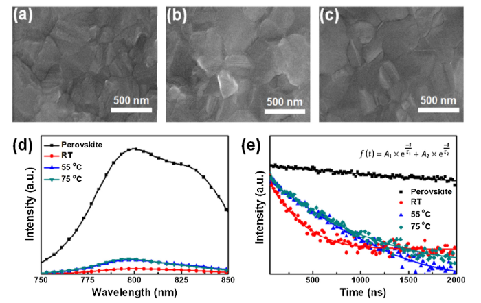
The perovskite absorber ((FAPbI3)0.95(MAPbBr3)0.05) was formed on thin film of ZrSnO4 NPs by anti-solvent quenching process [28]. Fig. 4(a-c) shows SEM images of the surface of the perovskite layers. Both three films exhibited a fully covered surface with dense grains sizing from 300 to 500 nm regardless of underlying ZrSnO4 layers. The electron extraction capability for ZrSnO4 with different fabrication temperature was studied by steady-state photoluminescence (PL) spectra. As shown in Fig. 4(d), the pristine perovskite shows a peak at 785 nm and this peak reduces when the ZrSnO4 layer is fabricated under perovskite layer. It means ZrSnO4 layer successfully transport carriers from perovskite layer. Moreover, the RT fabricated ZrSnO4 shows lower PL intensity as compared to other ZrSnO4. It can contribute to efficient electron extraction from perovskite layer to ETL. The electron lifetime process at the interface of perovskite and ZrSnO4 was analyzed by time-correlated single-photon counting (TCSPC) technique. (Fig. 4(e)) The average PL lifetime (τave) of the pristine perovskite absorber was 1398.64 ns, while the lifetime substantially decreased as the ZrSnO4 NPs were introduced as an ETL. The perovskite layer showed the lowest τave, of 116.79 ns with ZrSnO4 NPs (RT) while the other exhibited slightly elongated lifetime of 249 ns and 263.6 ns with ZrSnO4 NPs from 55 °C and 75 °C, respectively. The PL lifetime quenching primarily corresponds to the effective and quick charge extraction from perovskite, so the ZrSnO4 NPs from RT would be the most effective ETL in planar PSCs.
Fig. 4. SEM images of perovskite layers on ZrSnO4 nanoparticles synthesized at RT (a), 55 °C (b), and 75 °C (c). Steady state PL spectra (d) and time-resolved PL spectra (e) of the perovskite layer on ZrSnO4.
To explore the function of ZrSnO4 NPs as an ETL, the photovoltaic performance of planar heterojunction PSCs was studied in planar heterojunction architecture (ITO/ZrSnO4/perovskite layer/Spiro-OMeTAD/Au). The cross-sectional SEM image of a representative device was shown in Fig. 5(a). The thickness for ZrSnO4 NPs and perovskite absorber were ∼30 nm and ∼500 nm, respectively. Fig. 5(b) displays the current-voltage (J-V) curves of the champion device with different ZrSnO4 NPs under 1 sun illumination (AM 1.5 G), and the corresponding device parameters were summarized in Table 1. The PSCs with ZrSnO4 NPs (RT) exhibited the optimized PCE of 16.76 % with a VOC of 1.00 V, a JSC of 24.75 mA/cm2, and a fill factor (FF) of 0.67. For the ZrSnO4 NPs synthesized at the higher temperature, the PCEs decreased to 14.80 % and 14.50 % for the reaction temperature of 55 °C and 75 °C, respectively. The major improvement in the photovoltaic properties relied on the substantial enhancement of VOC and FF, which could be ascribed to the improved energy level alignment and thus reduced energy loss at ZrSnO4 and perovskite layer. Fig. 5(c) indicates that the photon-to-electron conversion efficiencies for different ZrSnO4 NPs were comparable.
Fig. 5. (a) Cross-sectional SEM image of device employing ZrSnO4 nanoparticles, (b) J-V curves and (c) EQE spectra of the devices with regard to ZrSnO4 synthesis temperature.
Table 1 Photovoltaic parameters for the planar heterojunction PSCs based on NiOX with various Zn doping concentrations.
| Temperature* [oC] | VOC [V] | JSC [mA cm-2] | JSC** [mA cm-2] | FF | PCE [%] | ηcc*** [%] | Rs [103 Ω] | Rsh [Ω] | R1 [Ω] | R2 [Ω] | R3 [Ω] |
|---|---|---|---|---|---|---|---|---|---|---|---|
| RT | 1.00 | 24.75 | 23.37 | 0.67 | 16.76 | 93.0 | 8.13 | 429 | 43.2 | 117 | 29.6 |
| 55 | 0.93 | 25.00 | 23.76 | 0.64 | 14.80 | 87.9 | 11.6 | 321 | 43.9 | 143 | 3.11 |
| 75 | 0.97 | 24.40 | 22.39 | 0.62 | 14.50 | 87.4 | 7.90 | 128 | 30.9 | 178 | 24.8 |
To elucidate the influence of the electrical properties of the devices, the recombination dynamics and charge transport properties were studied by using intensity-modulated spectroscopy technique. As shown in Fig. 6(a), the plots of time constants for the electron recombination lifetime (τr) to the VOC at varied illumination intensity, which was evaluated from IMVS. This result shows an increased order of τr of charge carriers in the device with an order of RT > 55 °C > 75 °C for ZrSnO4 NPs-based ETLs, which suggests the effectiveness of RT-synthesized ZrSnO4 NPs for suppressing the charge recombination at the interface of PSCs rather than the other ETLs. It has been reported that the degree of charge recombination is largely responsible for the observed increase of VOC in planar PSCs, which supports the reduced VOC for PSCs with ZrSnO4 NPs from 55 and 75 °C [29]. Fig. 6(b) shows electron transport lifetime (τt) for three devices in a short-circuit condition. The comparable τt for the devices indicate that the electron transport and extraction capabilities did not significantly influence by the synthesis temperature of ZrSnO4 NPs, which is further evident to the similar JSC and EQE results. It is also noted that the photo-induced charge carriers should be transported and extracted to the electrodes before recombination. Thus, charge collection efficiency (ηcc) can be estimated by the following Eq. (1).
ηcc=1-τt/τc (1)
Fig. 6. (a) Intensity modulated photocurrent spectroscopy, (b) intensity modulated photovoltage spectroscopy, (c) electrochemical impedance spectroscopy, (d) J-V curves under dark,of ZrSnO4-based PSCs.
As summarized in Table 1, ZrSnO4 NPs synthesized at RT achieved the highest charge collection efficiency of 93 % higher than others that remain ∼87 %. The high charge collection efficiency with the RT-synthesized ZrSnO4 NPs indicates beneficial alignment and thus faster electron transport capability with the selective contacts. This was further supported by impedance spectroscopy. Fig. 6(c) shows the Nyquist plots for three devices with different ZrSnO4 NPs-based ETLs under the dark condition with a bias (0.75 V), and the fitted results of the equivalent circuit are listed in Table 1. In the Nyquist diagram, the high-frequency intercept on the axis is referred to the series resistance (R1) in the device. In addition, the semicircle in high-frequency range can be referred to the charge transfer resistance (R2) at the interface for ZrSnO4/perovskite, while the main semicircle in the low frequency range is primarily relevant to the recombination resistance (R3) [30]. It is noted that the first semicircle in high frequency regime is not obviously distinguished because it merged into the second semicircle. As compared in R1 and R2 values for the devices, the most outstanding charge transport capability for RT-synthesized ZrSnO4 NPs was confirmed. The least R3 value of the ZrSnO4 NPs (RT)-based device further suggests the largest resistance in charge recombination at the interface of the device. These favorable electrical properties of the ZrSnO4 NPs synthesized at RT were further verified from the lowest leakage current at negative bias in dark, as well as the highest ideality factor. (Fig. 6(d)) Thus, we conclude that the electrical properties were modulated by controlling the synthesis temperature of ZrSnO4 NPs, which influences electron transport/recombination characteristics at the interface of PSCs. In specific, the RT-synthesized ZrSnO4 NPs afforded the optimized electron extraction and recombination, leading to the highest Jsc and FF than other ZrSnO4 NPs-based devices.
Another issue of importance to the practical usage of PSCs is long-term stability. To explore resistance of ZrSnO4 NPs-based devices to moisture, we monitored the PCE decay of the devices as the devices were stored in ambient condition. It is noted that the fresh devices were placed in high relative humidity condition at room temperature (27 ± 1 °C, relative humidity ∼75 %) without any encapsulation (Fig. S4). All the devices exhibited unsatisfactory stability against moisture, as shown in Fig. 7(a-d). After 48 h exposure in ambient condition, the devices retained less than 50 % of the initial PCEs. Thus, we understand that the ZrSnO4 NPs itself does not guarantee the ambient stability of the devices. The light stabilities of the devices were also investigated, as shown in Fig. 7(e-h). It is interesting that the devices employing RT-synthesized ZrSnO4 NPs still exhibited ∼50 % of initial PCE value under continuous 1 sun irradiation for 33 h, whereas the other devices were quickly degraded within 20 h. Despite the exact reasons for this discrepancy in light stability are not clear, it is suspected that better interfacial contact between the perovskite and ETL would play an important role in retaining long-term device stability against light.
Fig. 7. Stability results of PSCs with different ZrSnO4-based PSCs under ambient condition (a-d) and under N2 atmosphere with continuous illumination (100 mW/cm2) (e-h).
We herein reported the design and synthesis of highly crystalline and fine ZrSnO4 NPs at low temperature. The favorable optoelectronic properties of ZrSnO4 NPs such as high transparency, suitable energy levels and electronic structure were demonstrated for being used as an ETL in PSCs. The ZrSnO4 NPs-based ETLs have great potential for optimal electron transport and recombination at the interface of perovskite absorber layer, and the resulting devices achieved PCE as high as 16.76 % using the RT-synthesized ZrSnO4 NPs, which is a promising photovoltaic performance as solution-processed NPs-based ETL. Although the stability issue still remains in the ZrSnO4 NPs-based ETL, the low-temperature synthesized ZrSnO4 NPs will provide insight for designing the novel interfacial materials for PSCs. We believe that this study will be a seminal guide for designing functional ternary metal oxides for optoelectronic applications.
This research was supported by Korea Electric Power Corporation (Grant number: R17XA05-11) and Korea Basic Science Institute (KBSI) National Research Facilities & Equipment Center (NFEC) grant funded by the Korea government(Ministry of Education) (No. 2019R1A6C1010052). This work was also supported by the Basic Science Research Program through the National Research Foundation of Korea (NRF) funded by the Ministry of Science, ICT & Future Planning (Grant number: 2017R1C1B2009691).
Supplementary material related to this article can be found, in the online version, at doi:https://doi.org/10.1016/j.jmst.2019.11.008.

 WeChat
/
| 〈 |
|
〉 |


