Search for articles:
Qingfeng Zeng , Changhao Yang, Jiantao Liu
Corresponding authors:
Received: 2018-09-15
Revised: 2018-10-31
Accepted: 2019-04-14
Online: 2019-12-05
Copyright: 2019 Editorial board of Journal of Materials Science & Technology Copyright reserved, Editorial board of Journal of Materials Science & Technology
More
Abstract
Digital light processing technique was applied to manufacture alumina ceramic parts with two types of lattice structure units, i.e. vertex interconnect structure and edge structure. The internal porosity of the unit is 40%. The printed parts were sintered and the grain size is about 1.1 μm. The bending strength of the vertex interconnect structure is much larger than that of the edge structure. Materials genome initiative (MGI) aims to digital design and intelligent manufacture for advanced components. This research shows us an example to achieve this goal.
Keywords:
To speed up the material designs and applications, materials genome initiative (MGI) was put forward to achieve this goal. MGI tries to perform computational modeling and simulation before a real manufacturing for advanced materials.
Compared with metal materials, ceramic materials have many advantages, such as high strength, high temperature resistance, corrosion resistance and wear resistance [1]. Some ceramics also have unique electronic and magnetic properties. Thus, they have wide applications in chemical industry, aerospace, mechanical industry and electronic industry. Among ceramic materials, alumina ceramics have many excellent properties, including high elastic modulus, wear resistance, chemical corrosion resistance, high temperature stability and low raw material cost. It is a widely used high temperature structural material and wear resistant material [2].
With the development of high-performance ceramics, the requirements for the structure and dimensional accuracy of ceramic parts are increased in the engineering field [3]. Unfortunately, it is difficult to manufacture ceramic parts with complex structures using the traditional molding and machinery techniques [4].
Recently, additive manufacturing technology (3D printing) has been developed rapidly in forming and manufacturing complex ceramic parts [5]. Compared with the traditional ceramic molding method, this technology has the advantages of high precision, no need for mould, short development cycle and low manufacturing cost [6]. It has been applied to manufacture complex parts which has the character of hollow structure and thin wall, such as aircraft engine blade [7]. The additive manufacturing technology has broad application prospects in the aerospace, automotive, electronics, biomedicine and other fields [8].
Porous lattice structure materials have ever-changing microstructures and high porosity, and thus have excellent performances such as light weight, high strength, high efficiency heat dissipation, electromagnetic wave absorption, and designability [[9], [10], [11]]. Consequently, they have been widely used in many fields. Due to the limitations of the preparation process, a porous structure usually has an irregular overall distribution inside the material. With the rapid development of material preparation technology and 3D printing technology, the preparation of lightweight materials with controlled spatial position of porous structures and geometric features has gradually matured, which provides an experimental basis for studying the mechanical properties of porous lattice structures.
The porous lattice material simulates the molecular lattice configuration by computer-aided design, and the node and the connecting rod unit form a periodic topology. The lattice material composed of different cell structures exhibit a wide range of mechanical properties. Common three-dimensional lattice configurations include octahedron structure, tetrahedron structure, quadrangular pyramid structure, woven laminated sandwich structure, full triangular lattice structure, Kagome structure [12,13] and so forth. Many researches have been done on the relationship between the lattice structure and the relevant mechanical properties. Dede et al. [14] introduced a technique for designing single-layer or multi-layer periodic lattice structures, and further analyzed the mechanical properties of single-layer lattice structures. Tekoglu et al. [15] investigated the effect of cell size on the mechanical properties, through theoretical and numerical analysis of porous lattice materials under the compression, bending and shearing conditions. Zhong et al. [16] adopted the finite element method to analyze the mechanical properties of five typical cells, and proposed a design method for lattice materials under various loadings. Some pioneer simulation-based work have been performed to investigate the mechanical properties for 3D printed polymer and metal components [17,18]. On the other hand, there is very limited simulation and experimental combined research on 3D printed ceramic parts.
In this paper, we developed a feasible scheme to design and manufacture lattice materials from MGI point of view. We can get better model through model design. Then, the model can be quickly manufactured by 3D printing.
In this study, the alumina powder (Jiangsu Lianlian, Chemical Co., Ltd., China) of average particle size of 500 nm is adopted as an illustration of our scheme. The photosensitive resin consists of five basic components: oligomer(44 wt%), reactive diluent(39 wt%), photoinitiator(3 wt%), dispersant (5 wt%) and defoamers (9 wt%). The ceramic powder is added to the photocurable resin mentioned above and mixed well. The mixture consists of 80 wt% ceramic powder and 20 wt% photosensitive resin. The mixture is ball-milled for 8 h to make it fully mixed, so that we prepare a uniform ceramic suspension with a low viscosity and the solids content is 80 wt%. The ceramic suspension is poured into the trough of a 3D printer (Xi’an Particle Cloud Biotechnology Co., Ltd., China) using digital light processing (DLP) technology. Then, the DLP printer starts to form the ceramic green body, using the input parameters. The samples are heated to 1650 °C and maintained at a constant pressure for 4 h to make sure that the alumina ceramics are fully sintered.
Four samples were printed for each of the two different lattice structure models, and the sintered samples were polished to obtain specimens of 7 mm (W) ×8 mm (H) ×30 mm (L). The specimens were measured in flexural strength on a three point bending device (RGM-6300, Shenzhen Reger Instrument Co., Ltd., China) with a span of 12 mm and a cross-head displacement of 0.5 mm/min. The morphology of polished fracture of the samples was characterized by scanning electron microscopy (Apreo + HiVac, FEI, America).
In this paper, the cell structure derived from the cubic space microstructure is designed, and its mathematical model is established to construct the parametric model and analysis system of the sample. Fig. 1(a) shows the edge structure, consisting of 12 cylindrical edges forming a rectangular parallelepiped with general structural characteristics. Fig. 1(b) presents the structure of the interconnected vertices. The center of the cuboid is connected with 8 vertices through the pillars and the same vertex is connected in sequence. It enhances the endpoints of the vertex structure.
Fig. 1. Lattice structures under consideration: the edge structure (a) and the structure of the interconnected vertices (b).
In order to make the lattice structure composed of two different cells have the same outer dimensions and quality, it is necessary to ensure that the cell void ratio is the same, and the void ratio is computed by:
Above, the subscript n denotes a (edge structure) or b (interconnect vertex structure); Rn is the cross-section radius of the cell pillar; ln is the total length of the pillars in the cell structure; xn is the side length of the cubic space occupied by the cell structure.
The total lengths of different cell structural pillars are different. And it is known from the structural characteristics of each cell, that the sharing edges of the edge structure and the adjacent cell structures should be divided into four equally. The situation is also applied to the interconnect vertex structure. The total length of the cell pillar can be calculated with:
When designing the test models using the above cell structure, we ensure that the cell structure has the same side length (xn = 3 mm) and the cell internal void ratio (40%) is the same. Under this condition, the cross-section radius of the cell pillar of the edge structure is 0.757 mm, while the same parameter of the interconnect vertex structure is 0.439 mm.
Based on the parameterization results of the lattice structure, the COMSOL software package is used for the modeling and simulation. Each testing model (Fig. 2) consists of two layers of lattice structures, which is sandwiched by two 1 mm thick plate. The number of cell structures contained in the x and y directions of the test model is 10 and 2, respectively.
Fig. 2. Testing model designed with the edge structure (a) and the structure of the interconnected vertices (b).
Fig. 3 shows the resulting alumina components with lattice structure. Through DLP printing technology, we have realized the precise manufacture of complex ceramic materials. The material design based on the lattice structure keeps uniform sample structure. In this study, the sintered components have 21% controllable shrinkage compared to the printed ones, therefore the printed components are scaled upto 21%.
Fig. 3. Sintered alumina components designed with the edge structure (a) and the structure of the interconnected vertices (b).
The microstructure of the polished fracture surface of the sintered ceramic body at 1650 °C is visualized in Fig. 4. The microstructure of alumina ceramic samples is very dense because of the solids content as high as 80 wt%, though very few micropores present at the grain boundaries. The mean grain size of the alumina grains is 1.1 μm. The porosity can be controlled below 5%.
Fig. 4. Morphology of polished fracture of the alumina ceramic before (a) and after (b) sintering at 1650 °C.
The constraints for simulations are set as shown in Fig. 5. A formula is applied to consider the effect of porosity on the solid modulus of elasticity [19]:
Above, E is the effective elastic modulus, Es the solid phase elastic modulus (398 GPa), and p the porosity.
Fig. 5. Constraints used for simulations.
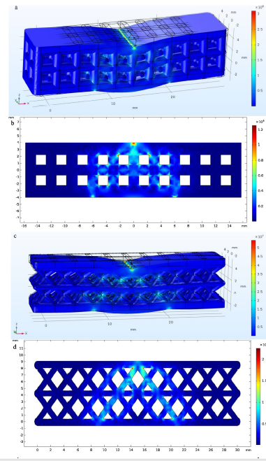
We got the stress distribution (Fig. 6) and the load-deflection relationship during linear deformation in a three-point bending test by simulation (Fig. 7). As Fig. 6 shows, the stress distribution of the interconnect vertex structure is more uniform than that of the edge structure. Through the three-point bending test, we measured the bending strength of the alumina ceramic samples. The average bending strength of the sample with the edge structure is 17.52 MPa. The average bending strength of the sample with the vertex interconnect structure is 28.96 MPa, which is much better than the edge structure. We also get the load-deflection curve (Fig. 8). And the curve shows consistency with our simulation results. When the same load is applied, the deformation of the vertex interconnect structure is bigger than that of the edge structure. However, the vertex interconnect structure can bear much more deformation than the edge structure. Therefore, the vertex interconnection structure has stronger bending strength. Meanwhile, the figures indicate that, under the same loadings, the simulated disturbance value is slightly lower than that obtained by the test. This difference is reasonable. Defects in the material will result in a slight decrease in the performance of the material.
Fig. 6. Stress distribution of the edge structure (a) (b) and the structure of the interconnected vertices (c) (d) (N/m2).
Fig. 7. Loading vs deflection curve obtained from simulation.
Fig. 8. Loading vs deflection curve obtained from the three-point bending test.
With the help of the DLP printing technology, we realized the precise and rapid manufacturing of complex components. The alumina ceramic components molded with our scheme have excellent structural uniformity after being sufficiently sintered. Alumina grain size can be controlled at around 1.1 μm. Different lattice structures allow the components to have different mechanical properties. The bending strength of the vertex interconnect structure is much larger than that of the edge structure. MGI aims to digital design and intelligent manufacturing for advanced components. This research shows us an example to achieve this goal, and we believe this method can be adopted to other properties of materials.
We thank the National Key R&D Program of China (Grants Nos. 2017YFB0703200, 2016YFB0700500), the National Natural Science Foundation of China (Grants Nos.51372203, 51332004, 51571166, 51972268 and 51761135032), the Foreign Talents Introduction and Academic Exchange Program (Grant No. B08040) for their financial supports. We also thank Mr. Xiaolong Zhao from Xi’an Particle Cloud Biotechnology Company for his assistance with DLP printing.

 WeChat
/
| 〈 |
|
〉 |


