1 Department of Electronics and Key Laboratory of Photo-Electronic Thin Film Devices and Technology of Tianjin, Nankai University, Tianjin 300071, China
2 School of Material Science and Engineering, Hebei University of Technology, Tianjin 300130, China
3 Institute of Material Physics, Key Laboratory of Display Materials and Photoelectric Devices, Tianjin University of Technology, Tianjin 300384, China
4 Tianjin Key Laboratory of Composite and Functional Materials and School of Materials Science and Engineering, Tianjin University, Tianjin 300072, China
5 Key Laboratory of Optical Information Science and Technology, Ministry of Education, Institute of Modern Optics, Nankai University, Tianjin 300071, China
Photo-corrosion is one of the major obstacles for CdS application in wet chemical fields, and atomic layer deposition (ALD) has been proposed as an effective way to suppress the corrosion. Here, prior to ALD coating, CdS, one facilely corrosive photocatalyst, was synthesized via hydrothermal synthesis to access the fundamental corrosion mechanism and the according corrosive sites. X-ray photoelectron spectroscopy (XPS) and X-ray diffraction (XRD) demonstrated that the failure of catalytic decomposition of methylene blue originated from the formation of soluble CdSO4 by oxidizing S2- of as-prepared CdS. High resolution transmission electron microscopy (HRTEM) further identified the active sites in the V-shaped regions of CdS nanoparticles, confirmed by the simulated electric field distribution. To rationally coat oxides on CdS, the right candidates and their thicknesses have been considered by our tunneling model with transfer matrix method based on quantum mechanism, upon which the thickness of protective layer should be less than 0.5 nm to maintain a high tunneling probability, and thus one cycle of ALD TiO2 or Al2O3 was proposed to passivate the CdS powder to balance the carrier transportation and corrosion suppression. Based on HRTEM results, we found that the active V-shaped region was covered by ALD oxides (TiO2 or Al2O3). For each case, no soluble CdSO4 has been found before and after photocatalytic reactions based XPS measurements. Importantly, we noticed that with the passivation of one cycle of ALD, the catalyst's lifetime was elongated up to >14 times higher than that of the as-prepared CdS.
Photocatalysis is one of the promising technologies to solve the increasing problems of energy shortage and environmental pollution. TiO2 is one of the most studied catalysts due to its superior properties, such as low cost and high stability. Nevertheless, the wide band gap (~3.2 eV) of anatase TiO2 results in a waste of ~95% solar energy[1, 2]. In order to ultimately improve the efficiency of harvesting solar energy, it is urgent to develop visible-light photocatalyst. Metal oxides with narrow band gaps, such as WO3 (2.6 eV)[3, 4] and Fe2O3 (1.9-2.2 eV)[5, 6], have attracted extensive attention, whereas their conduction band minimum (CBM) is normally more positive than the redox potential of H+/H2 (0 V vs. NHE) to degrade organic pollution or produce H2 unless heterojunction is produced[7, 8].
Compared to metal oxides, metal sulphide semiconductor photocatalysts could meet the requirement of band alignment between catalyst's band edges and water redox potentials. Cadmium sulfide (CdS) (2.4 eV)[9] has thus been regarded as one of the promising candidates for organic photodegradation[10] and H2 evolution[11]. Nevertheless, the serious photo-corrosion inhibits its wide applications[12, 13]. Previous investigation reveals that this photo-corrosion of CdS is initiated by the reaction of photo-generated holes with active sites and S2- is consequently photo-oxidized under illumination[14, 15]. However, it remains inaccessible how to identify active sites when considering the variation of the shapes of CdS nanoparticles. In order to prevent the photo-corrosion, atomic layer deposition (ALD) technology[16] has been adopted to deposit 2-100 nm protective layer (such as TiO2[17, 18], Ta2O5[19], etc.) on photo electrode plate by multiple ALD cycles to passivate photocatalyst surface and suppress photo-corrosion in the photocatalytic field. For the ALD protective layer, it could not be either too thick to decrease the out-diffusion of excited carrier or too thin to protect the active sites. Therefore, a rational design of ALD layer is indispensable to obtain a reasonable protective layer.
In this work, we found that the loss of catalytic sites arose from the formation of soluble CdSO4 in the highly active V-shaped regions of CdS nanoparticles, which were synthesized with hydrothermal method. The calculation of electric field distribution helped to understand the charge distribution of V-shaped regions and thus determined the active area. To rationally design the protective layer and thus suppress photo-corrosion of active sites, the tunneling probability of photo-generated carriers between protective layer (TiO2 or Al2O3, thickness from 0.1 nm to 2 nm) and CdS has been calculated by a tunneling model with transfer matrix method based on quantum mechanism. According to the theoretical insights, the thickness of protective layer should be less than 0.5 nm to maintain the high tunneling probability and photocatalytic efficiency. Therefore, without introducing any precious metal co-catalyst, to reduce cost and save time, one cycle of ALD TiO2 or Al2O3 passivation layer was deposited on CdS powder surface to significantly increase the lifetime of the catalyst. These findings provide fundamental understanding of active sites photo-corrosion process and shed light on the rational design of protective layer for ALD passivating photocatalyst to preserve its photocatalytic activity.
2. Experiment and Calculation Methods
2.1. CdS sample preparation, structural characterization and ALD passivation process
The hydrothermal synthesis method was used to fabricate CdS nanoparticles. An aqueous solution of 0.025 mol cadmium acetate, 0.075 mol thiourea, 0.005 mol sodium lauryl benzenesulfate, and 0.2 mol ammonia was sealed in a Teflon-lined stainless autoclave of 50 mL, kept at 120 ° C for 2 h, and then cooled to room temperature. The precipitates were separated by high-speed centrifuge at 10 000 rpm for 5 min, and rinsed by sequential centrifugation/redispersion from/in deionized water (DI water) 5 times to remove redundant impurity completely, and finally dried in the oven at 70 ° C for 12 h. X-ray diffraction (XRD, D/max-2500, Rigaku), high resolution transmission electron microscopy (HRTEM, JEM-2100, JEOL), and X-ray photoelectron spectroscopy (XPS, PHI-5300ESCA, PHI) were used to identify the phase, particle size and chemical state of CdS, respectively. In the ALD process, the ALD system (Type: f-100, WUXI MNT MICRO AND NANOTECH CO., LTD.) was used to deposit the TiO2 and Al2O3. The Tetrakis(dimethylamino)titanium (TDMAT) and trimethylaluminum (TMA) were used as metal precursors to deposit TiO2 and Al2O3, respectively. Water vapor was used as the oxidant precursor. The deposition temperature was kept at 150 ° C. Each ALD cycle consisted of a 50 ms pulse of TDMAT, followed by a 20 ms pulse of H2O for TiO2 deposition. For Al2O3 deposition, each ALD cycle consisted of a 20 ms pulse of TMA, followed by a 20 ms pulse of H2O. A 25 s purge under a constant 20 sccm flow of research-grade N2 (g) was performed between each precursor pulse.
2.2. Photocatalytic activity measurements
The photocatalytic performance was examined by degradation of methylene blue (MB). Forty milligrams of CdS powders were dispersed in MB solution (100 mL, 10 mg/L) in a water-cooling beaker, and the photocatalytic reaction temperature was kept at 25 ° C. Then it was stirred for 30 min in the dark to reach adsorption-desorption equilibrium. A xenon lamp without filter was used as a simulation sunlight source to trigger the photocatalytic reaction, and the focused intensity was ~75 mW/cm2, which was measured by an irradiance meter (Model: S302-C, Thorlabs). During photodegradation of MB solution, the magnetic stirring kept running. The photodegradation was quantified by monitoring the concentration of MB at its absorption maximum (664 nm). For the photodegradation experiment, the experimental time lasted 3.5 h for 1 photocatalytic round, and then the catalyst was recycled by centrifugation and cleaned by ultrasonication in DI water. The recycled catalyst was used in the 2nd photocatalytic test. Likewise, the same method was used for the 3rd and 4th rounds of photocatalytic measurements. The same amount in weight of commercially available Degussa P25 (nanoscale TiO2 powder; 80% anatase, 20% rutile; particle diameter: 25-30 nm), as a reference, was used to compare with the photocatalytic performance of CdS.
2.3. Calculation of electric field distribution
The x-y and x-z distributions of normalized electric field amplitude for the CdS particles were obtained with the finite element method (FEM) [20]. The calculation was performed with the COMSOL Multiphysics software. The CdS particle with a radius of 25 nm was illuminated by a plane wave that propagated along horizontal z-direction and polarized along vertical x-direction with a wavelength of λ = 500 nm. The electric field amplitude of the incident plane wave was normalized to be unitary. On one side of the particle, a circular cone with a cone angle of 120° , a height of 5 nm, and the cone axis along the x-direction were digged out to form the V-shaped defect. The refractive index of CdS under the illumination wavelength of 500 nm is 2.7 + 0.7i[21]. The results exhibited an enhancement of electric field in the vicinity of the circular cone, and the field at the outside edge of the cone was stronger than that at the inside edge.
2.4. Tunneling probability calculations
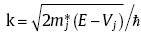
For a semiconductor heterojunction, band bending takes place when two semiconductor materials come to contact. The bending band, i.e., quantum well/barrier, in the depletion region determines the carrier transmission between two materials. In order to quantify the carrier tunneling at the interface, one needs to solve the Schrodinger equation with a reasonable quantum well/barrier potential term, which well describes the band bending. The potential shape is essentially controlled by the materials' dielectric constant and doping concentration[22]. In this work, we proposed a simple, accurate, and fast algorithm for numerically solving the Schrodinger equation in quantum-well/barrier structures, based on the transfer matrix method (TMM).
The TMM technique divided any arbitrary potential into numerous discrete rectangle segments. For each segment, the potential V was uniquely determined, and subsequently wave function boundary condition was applied to obtain the carrier tunneling probability through the whole arbitrary potential. In such a way, the transportation probability of excited carriers could be quantified via the TMM technique [23].
Specifically, for a one-dimensional steady state in this work, Schrodinger equation is expressed as,
where E and V represent the eigenvalue and the potential term, respectively. m* is the effective mass. For any shape of potentials, the TMM technique divided V into N rectangle segments, each of which could be small enough to be treated as a fixed value.
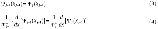
For any segments, wave function was expressed as
Where , and Aj and Bj are the coefficients of the forward and the backward wave functions, respectively.
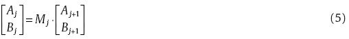
The boundary conditions for the wave functions and the first-order of wave function derivatives between two segments were written as[24]:
Here, mj* is the effective mass of the corresponding segment.
Applying the boundary conditions to Eq. (2), we obtained the coefficient relationship between any two adjunct segments:
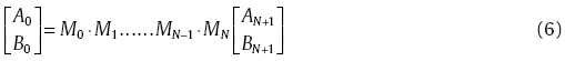
where Mj is a 2 × 2 matrix. With Eq. (5), we found a relation between the A and B coefficients of the outermost layers:
equation(6)
where
where , N is the position of segment N.
Inserting MN into Eq. (6), we simplified it as Eq. (8):
Here, BN+1 is zero since there is no reflect wave after transferring through the potential barrier/well. Finally, the transmission coefficient T (E) was obtained as follows:
With this expression, carrier transmission probability could be determined for any shape of potentials.
3. Results and Discussion
3.1. Characterization of as-prepared sample
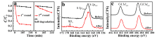
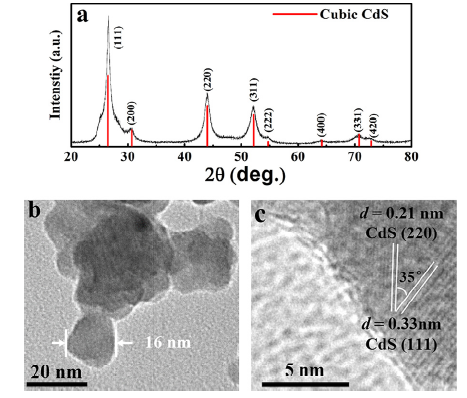
The pure cubic phase of the as-prepared CdS nanoparticles was identified by XRD as shown in Fig. 1(a). TEM image exhibits the particle sizes varying from 10 to 20 nm in Fig. 1(b). The HRTEM (Fig. 1(c)) that shows the major facet of cubic CdS nanocrystal is the (111) plane with d(111) spacing of 0.33 nm owing to its low surface energy[25].
Fig 1. (a) XRD patterns, (b) TEM and (c) HRTEM images of as-prepared CdS nanoparticles
3.2. Photodegradation of MB by as-prepared sample and failure mechanism
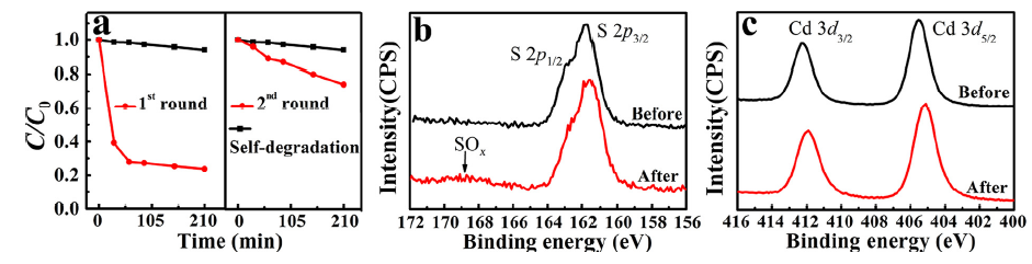
To examine the photocatalytic performance, CdS (40 mg) was dispersed in MB solution. In Fig. 2(a), the self-degradation of MB under irradiation was very small and can be negligible. After introducing CdS into the MB solution, high degradation efficiency of MB was observed and more than 70% MB was degraded in 60 min. The high efficiency is related to CdS's superiority of its light adsorption in the visible light range and band alignment with water redox potentials. However, after 60 min, no further catalytic activity was observed, resulting from the loss of active sites. Subsequently, the catalyst was recycled and cleaned in DI water by ultrasound, and no more obvious MB decomposition was found, and thus we concluded that the photo-corrosion indeed caused the photocatalytic failure.
Fig 2. (a) Photodegradation of MB by CdS nanoparticles without ALD passivation; (b) S 2p and (c) Cd 3d of CdS before and after photocatalytic reactions.
To access the failure mechanism of the catalyst, XPS measurements were carried out to study the surface chemistry before and after photocatalytic reactions. An SOx broad peak around 169 eV was identified as the S 2p core level spectra after 1 hour photocatalytic reaction, which suggests the S2- being oxidized into SOx ( Fig. 2(b)). Meanwhile, no detectable changes of Cd 3d core level spectra were observed before and after the photocatalytic reactions ( Fig. 2(c)), arising from the overlapping of Cd peaks between CdS and CdSO4[26]. Fundamentally, CdS is a natural n-type semiconductor, in aqueous environments, and valence band up-bending occurs due to the majority carriers' out-diffusion when interfacing with water[27]. Consequently, the photo-excited holes from valence band maximum, mainly composing of S 2p orbitals [28], tend to transfer to the nanoparticles surface, then directly react with MB and essentially lead to the decomposition of MB pollutants. However, when soluble CdSOx formed during the photocatalysis process, the active element S lost and the photocatalytic activity decreased. This finding is consistent with previous work on photo-corrosion [29]. Nevertheless, to date, there is no report to discuss about the active sites of CdS.
3.3. Photocatalytic active sites identification
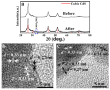
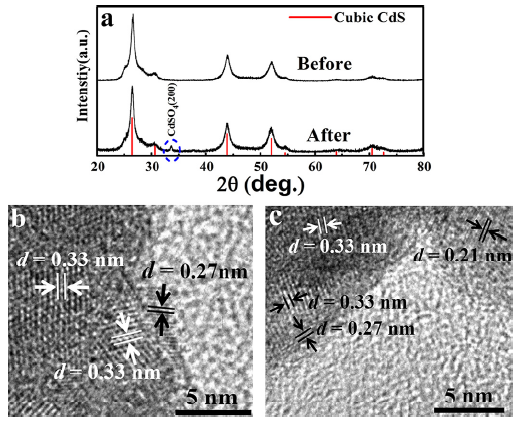
Without considering shape variation of the as-prepared spherical nanoparticle, the excited holes (electrons) move outward (inward), respectively, due to the band bending[30]. In practice, the shape variation is inevitable to influence the excited charge distribution and consequently impact the active areas. In order to locate these active sites, XRD and TEM were combined to characterize the surface modification on CdS nanoparticles after photocatalysis. The CdSO4 (200) peak emerges in XRD pattern (Fig. 3(a)) after the photocatalytic reactions since the S2- anion is oxidized into SO42- by the strong oxidizing excited holes. Surprisingly, only in the V-shaped areas of either one nanoparticle or overlapping of two particles CdSO4 (d200 = 0.27 nm) phase was found on surface in HRTEM images (Fig. 3(b) and (c)). On the other regions of the CdS nanoparticles, CdSO4 was not observed. Therefore, we speculated that the active sites were located in the V-shaped areas. Similar catalytic phenomenon dependence on the V-shaped regions has been observed in NaTaO3 catalyst[31].
Fig 3. (a) XRD patterns of CdS before and after photocatalytic reactions; (b) and (c) HRTEM images of the V-shaped regions of the CdS surface after photocatalytic reactions
3.4. Electric field distributions
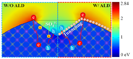
To identify the photocatalytic active sites, we calculated the electric field distribution of CdS nanoparticle whose shape and size are analogous to those in TEM images of Fig. 1(b) and HRTEM images in Fig. 3(b) and (c). It is well known that for a spherical shape of nano-particle, the electric field of outmost shell is distributed evenly. Here, we explored the charge distribution of a sphere with V-shaped defect. According to the electromagnetic field simulation (Fig. 4), the corners of CdS display strong electromagnetic (EM) field intensity, whereas in the V-shaped areas much lower EM intensity is distributed. The majority carriers of CdS, i.e electrons, gather at the corners due to the strong build-in internal electric field between the semiconductor and solution. On the contrary, the excited holes prefer to transfer into the V-shaped regions where we find the low EM field intensity resulting from the low electron concentration and recombination rate. Under this condition, photodegradation occurs in the active V-shaped areas. This finding helps to explain why photo-corrosion takes place in the V-shaped regions (Fig. 4, W/O ALD).
Fig 4. Distributions of normalized electric field amplitude for the CdS particle with a V-shaped defect under illumination by a plane wave and schematics of charge transfer without (W/O) and with (W/) ALD process
3.5. Tunneling probability of photo-generated carriers
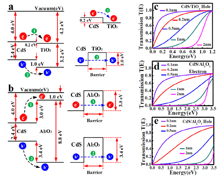
In order to suppress the photo-corrosion and maintain high photocatalytic efficiency, ultrathin coating passivation was performed by ALD (Fig. 4 W/ALD). Prior to ALD, we theoretically designed the ALD oxides with various thicknesses to deposit on CdS to protect the catalytic active sites. To examine how different protective layers impact the photocatalytic performance, we proposed the band alignment between CdS and TiO2 (Al2O3) based on the work functions. Subsequently, we developed a code with transfer matrix method (TMM) in quantum mechanics to calculate the excited carriers' tunneling probability between two semiconductors. The tunneling probability is proportional to exp (× a) (“ U” is the barrier height, “ E” is the excited carriers energy, “ a” is the barrier width); therefore, material properties and protective layer thickness are two crucial factors to govern the tunneling probability.
To simplify the problems, we considered the step potentials rather than quadratic ones between CdS (me* = 0.21 m0, mh* = 0.80 m0, m0 is free electron mass)[32] and oxides (TiO2 (me* = 0.0948 m0, mh* = 0.1995 m0)[33], Al2O3 (me* = 0.20 m0, mh* = 0.25 m0)[34]). As shown in Fig. 5(a), band alignment between CdS and TiO2 displays that CBM is higher than its TiO2 counterpart, and visible light excited electrons readily transfer to TiO2 side, whereas the holes need to overcome an energy barrier to out-diffuse. The valence band offset (VBO) between these two materials is around 1.0 eV (Fig. 5(a)), which was simplified as a square-shaped barrier. As we discussed above, the height of the barrier is determined by material property and the width could be a variable during the ALD growth process. In this work, we varied the oxide thickness from 0.1 nm to 2 nm to check how the oxide layer influences the tunneling probability. In Fig. 5(c), we found that tunneling could easily occur with the thickness less than 0.5 nm. With the increase in thickness, the tunneling probability decreases exponentially. With 2 nm thickness, the energy of 0.9 eV plus CdS band gap (2.4 eV) is needed to excite the hole carrier. Equivalently, visible light could not enable the hole diffusion. In the case of Al2O3/CdS, CB and VB offsets are around 3.0 eV and 3.4 eV, respectively (Fig. 5(b)). Likewise, we calculated the square-shaped barriers for these two offsets. Based on the calculations in Fig. 5(d) and (e), only thickness less than 0.2 nm could be favorable for carrier to diffuse due to the large offset. Compared to these two protective layers, the hole tunneling probability of TiO2 is higher than Al2O3 due to the low VBO potential barrier in TiO2/CdS heterostructure. In practice, band bending would occur, and the bending will slightly increase the hole tunneling probability.
Fig 5. (a) and (b) Band alignment of CdS/TiO2 and CdS/Al2O3, respectively; (c) tunneling transmission probability of hole for CdS/TiO2; (d) and (e) tunneling transmission probability of electron and hole, respectively, for CdS/Al2O3.
3.6. Characterization of ALD passivated sample
Guided by the theoretical insight from TMM, the thinner protective layer provides a higher tunneling probability, and the thickness of protective layer should be less than 0.5 nm to maintain the high photocatalytic efficiency. Therefore, one cycle of ALD on these CdS nanoparticles was adopted to passivate the active regions[35]. ALD, a self-limiting deposition technique for producing thin films, has been regarded as one promising way to precisely control film thickness and conformal grow of complex nanostructures[18]. However, initial growth mechanism is quite complex associated with activity sites on the sample surfaces. For example, it is difficult to incubate on MoS2 surface, but it can conformably grow uniform film after ozone pretreatment because of the surface oxygen absorbed[36]. Therefore, the surface active sites in the V-shaped regions of CdS nanoparticles should also provide the initial sites for incubation of ALD.
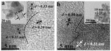
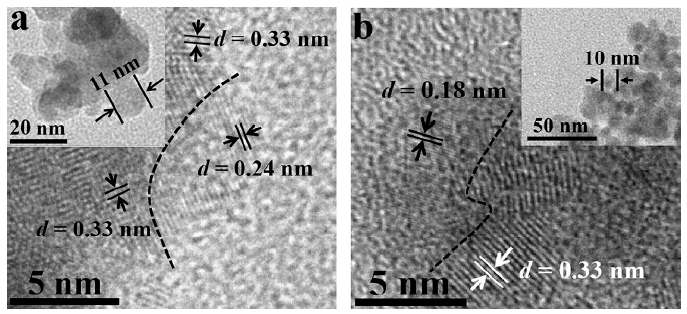
Fig. 6(a) and (b) show the HRTEM images after one cycle of ALD TiO2 and Al2O3, respectively. No significant grain size increase of CdS nanoparticles (10-20 nm) was observed after the ALD growth at low temperature (150 ° C)[37]. Upon one cycle of ALD, the TiO2 or Al2O3 crystalline phase could not be found in most areas from TEM results, and Ti or Al signal is below the XPS detection limit (see details in Fig. S1), attributing to less concentration of ALD oxides because of the inert cubic CdS (111) surface (d111 = 0.33 nm), which is consistent with theoretical calculations[24] and the lack of oxide signal from the XPS core level spectra of S 2p and Cd 3d for the as-prepared samples. But in some active areas with under-coordinated bonds, ALD layer could be formed. From Fig. 6, TiO2 (d101 = 0.24 nm) or Al2O3 (d024 = 0.18 nm) phase was identified in the V-shaped regions of CdS nanoparticles. These crystalline phase formation could be because of the trap of precursors in the V-shaped regions and subsequently experiencing high energy beam during the TEM measurement in the specific regions. It is worth to note that only five samples out of fifty with V-shaped regions were found to have the detectable TiO2 or Al2O3 phases. In other words, on most reactive V-shaped regions, crystalline phase was not observed, resulting from the self-limiting nature of ALD. This observation is consistent with the fact that Ti and Al core level signals are below the XPS detection limit after one cycle of ALD. Therefore, we assumed that the active V-shaped regions were covered with the ALD layer but only a small portion was detectable. The ultrathin ALD oxides could help to protect the active areas and thus elongate the lifetime of CdS catalyst.
Fig 6. HRTEM images of (a) CdS/1 cycle of ALD TiO2 and (b) CdS/1 ALD cycle Al2O3
3.7. Photodegradation of MB by passivated sample
Forty milligrams of passivated samples (CdS/one ALD cycle TiO2 or CdS/one ALD cycle Al2O3) were dispersed in MB solution to examine the photocatalytic performance and the catalyst lifetime.
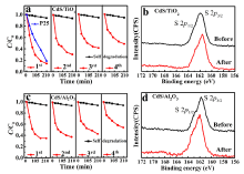
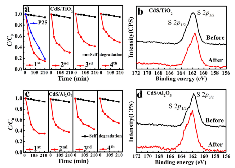
As shown in Fig. 7(a), CdS with one ALD cycle TiO2 shows great catalytic performance to decompose MB under illumination. As time went by from 0 min to 210 min, MB degradation was up to 90% gradually, which displayed a superior performance than the same amount of the commercially available P25. Most importantly, the catalyst lifetime was significantly improved compared with the as-prepared CdS. Furthermore, we tested three more rounds of MB degradations with 210 min per round (see Fig. 7(a)). We observed that overall degradation rate slightly reduced from round one to round four. We speculated that this performance reduction could have partly resulted from catalyst loss when recycling catalyst (left ~5 mg after 4 cycles). During the 4th round test, 50% MB pollutant can be degraded in 210 min. Interestingly, no new product was observed above the XPS detection limit after 4 rounds (14 h) of tests. In any case, the catalyst still remained active after 14 hours. In other words, the catalyst lifetime was elongated up to at least 14 times longer than that of the as-prepared CdS. One ALD cycle Al2O3 on CdS was also used to check catalytic performance variation in contrast to TiO2 deposition. For the CdS/one ALD cycle Al2O3 sample, MB degradation was up to 65% gradually after the 1st round (Fig. 7(c)), and it showed lower efficiency compared to CdS/one ALD cycle of TiO2 sample. This result agrees well with the TMM prediction. After the 4th round test, the catalyst still remained active for the MB degradation and new product also was not observed in XPS spectrum (Fig. 7(d)), similar to the result of CdS/one ALD cycle of TiO2 sample. In addition, to further verify the TMM calculated results, the sample of CdS with two ALD cycles TiO2 was also used to test the photocatalytic activity and showed the lower efficiency than CdS with one ALD cycle TiO2 (see details in Fig. S2) due to the decrease of carrier tunneling probability when the thickness increases. Qualitatively, we believe that the TMM calculated results can provide the rational guidance to a reasonable design of protective layer for ALD passivating photo-catalyst to suppress photo-corrosion.
Fig 7. (a) CdS/1 ALD cycle TiO2 and P25 for cyclic photo degradation MB; (b) S 2p of CdS/1cycle ALD TiO2 before and after photo catalytic reactions; (c) CdS/1ALD cycle Al2O3 for cyclic photo degradation MB; (d) S 2p of CdS/1cycle ALD Al2O3 before and after photocatalytic reactions.
In the ALD process, the V-shaped regions were partially covered with ultrathin TiO2 or Al2O3, and consequently the active sites were protected. As the protective layer was conformal to V-shaped activity sites and thin enough (< ~0.5 nm), the excited holes could be tunneling through the passivation layer and react with organic pollutants (Fig. 4 W/ALD); thus, the photocatalytic efficiency was maintained. The excited electrons tend to move in the opposite directions, whereas the accumulated electrons also tend to move out by diffusion. In any case, the excited electrons do not play a role to decompose MB[38]. To evaluate the catalytic role of carriers (electron/hole), we utilized alcohol to exhaust the supply of excited holes, and we found that MB degradation with alcohol is the same as that of the self-degradation under UV-vis light (see details in Fig. S3). This experiment confirms that the hole is the active carrier.
4. Conclusion
In conclusion, to prevent the photo-corrosion of CdS nanoparticles in the photocatalytic process, guided by TMM calculations, one cycle of ALD TiO2/Al2O3 treatment was employed to protect the active sites, which were located in the V-shaped regions of CdS nanoparticles. Simultaneously, a large proportion of photo-generated holes transfers to the nanoparticle surface by tunneling through the thin ALD oxides and maintains the high catalytic efficiency. This work sheds light on rational design of protective layer to preserve active sites of photo-catalyst for organic pollution reduction or water splitting.
Appendix. Supplementary material
AcknowledgementsAcknowledgments
This work is supported by the National Natural Science Foundation of China (Nos. 11304161, 11104148, 21573117, 51171082, 11404172 and 61322508), the 1000 Youth Talents Plan, the Tianjin Natural Science Foundation (Nos. 13JCYBJC41100 and 14JCZDJC37700), the National Basic Research Program of China (973 Program, Nos. 2014CB931703 and 2013CB328701), and the Fundamental Research Funds for the Central Universities.
W. M. Zhang, Y. Q. Jiang, X. Y. Cao, M. Chen, D. L. Ge, Z. X. Sun, Mater. Res. Bull, 48(2013), pp. 4379-4384[本文引用:1]
[11]
Q. Li, B. D. Guo, J. G. Yu, J. R. Ran, B. H. Zhang, H. J. Yan, J. R. Gong, J. Am. Chem. Soc, 133(2011), pp. 10878-10884[本文引用:1]
[12]
H. Zhu, R. Jiang, L. Xiao, Y. H. Chang, Y. J. Guan, X. D. Li, G. M. Zeng, J. Hazard. Mater, 169(2009), pp. 933-940[本文引用:1]
[13]
R. Wang, D. Xu, J. Liu, K. W. Li, H. Wang, Chem. Eng. J. , 168(2011), pp. 455-460[本文引用:1]
[14]
D. J. Fermin, E. A. Ponomarev, L. M. Peter, J. Electronal. Chem, 473(1999), pp. 192-203[本文引用:1]
[15]
T. Awatani, A. J. Mcquillan, J. Phys. Chem. B, 102(1998), pp. 4110-4113[本文引用:1]
[16]
B. J. O. Neill, D. H. K. Jackson, J. C. Lee, C. Canlas, P. C. Stair, C. L. Marshall, J. W. Elam, T. F. Kuech, J. A. Dumesic, G. W. Huber, ACS Catal, 5(2015), pp. 1804-1825[本文引用:1]
[17]
S. Hu, M. R. Shaner, A. Joseph, M. Lichterman, B. S. Brunschwig, N. S. Lewis, Science, 344(2014), pp. 1005-1009[本文引用:1]
[18]
Y. W. Chen, J. D. Prange, S. Dühnen, Y. Park, M. Gunji, C. E. D. Chidsey, P. C. McIntyre, Nat. Mater, 10(2011), pp. 539-544[本文引用:2]
[19]
C. C. Li, T. Wang, Z. B. Luo, D. Zhang, J. L. Gong, Chem. Commun, 51(2015), pp. 7263-7406[本文引用:1]
[20]
A. Chiba, K. Isaka, M. Kitagawa, T. Matsuo, M. Nagata, Y. Yokoi, Power Eng. Rev, 103(1984), pp. 1895-1902[本文引用:1]
[21]
F. Lisco, P. M. Kaminski, A. Abbas, K. Bass, J. W. Bowers, G. Claudio, M. Losurdo, J. M. Walls, Thin Solid Films, 582(2015), pp. 323-327[本文引用:1]
[22]
M. R. Shaner, K. T. Fountaine, S. Ardo, R. H. Coridan, H. A. Atwater, N. S. Lewis, Energy Environ. Sci, 7 (2) (2014), pp. 779-790[本文引用:1]
[23]
B. Jonsson, S. T. Eng, J. Quant. Elec, 26(1990), pp. 2025-2035[本文引用:1]
[24]
D. Y. Ko, J. C. Inkson, Phys. Rev. B, 38(1988), pp. 9945-9951[本文引用:2]
J. Riga, J. J. Verbist, P. Josseaux, A. K. Mesmaeker, Surf. Interface Anal, 7(1985), pp. 163-168[本文引用:1]
[27]
M. G. Walter, E. L. Warren, J. R. McKone, S. W. Boettcher, Q. X. Mi, E. A. Santori, N. S. Lewis, Chem. Rev, 110(2010), pp. 6446-6473[本文引用:1]
[28]
Y. N. Xu, W. Y. Ching, Phys. Rev. B, 48(1993), pp. 4335-4351[本文引用:1]
[29]
D. Meissner, R. Memming, B. Kastening, J. Phys. Chem, 92(1988), pp. 3476-3483[本文引用:1]
[30]
M. Grätzel, Nature, 414(2001), pp. 338-344[本文引用:1]
[31]
K. Hideki, A. Kiyotaka, K. Akihiko, J. Am. Chem. Soc, 125(2003), pp. 3082-3089[本文引用:1]
[32]
C. Y. Liu, A. J. Bard, J. Phys. Chem, 93(1989), pp. 3232-3237[本文引用:1]
[33]
J. F. Zhang, P. Zhou, J. J. Liu, J. G. Yu, Phys. Chem. Chem. Phys, 16(2014), pp. 20382-20386[本文引用:1]
[34]
A. Padovani, L. Larcher, V. DellaMarca, P. Pavan, H. Park, G. Bersuker, J. Appl. Phys, 110(2011), p. 014505[本文引用:1]
[35]
H. Tiznado, D. Domínguez, F. Muñoz-Muñoz, J. Romo-Herrera, R. Machorro, O. E. Contreras, G. Soto, Powder Technol, 267(2014), pp. 201-207[本文引用:1]
[36]
L. X. Cheng, X. Y. Qin, A. T. Lucero, A. Azcatl, J. Huang, R. M. Wallace, K. Cho, J. Kim, ACS Appl. Mater. Interfaces, 6(2014), pp. 11834-11838[本文引用:1]
[37]
J. R. Wank, S. M. George, A. W. Weimer, Powder Technol, 121(2001), pp. 195-204[本文引用:1]
[38]
H. Sheng, Q. Li, W. H. Ma, H. W. Ji, C. C. Chen, J. C. Zhao, Appl. Catal. B, 138(2013), pp. 212-218[本文引用:1]
1
1972
0.0
0.0
... 2 eV) of anatase TiO2 results in a waste of ~95% solar energy[1,2] ...
1
2012
0.0
0.0
... 2 eV) of anatase TiO2 results in a waste of ~95% solar energy[1,2] ...
1
2007
0.0
0.0
... 6 eV)[3,4] and Fe2O3 (1 ...
1
2001
0.0
0.0
... 6 eV)[3,4] and Fe2O3 (1 ...
1
2012
0.0
0.0
... 2 eV)[5,6], have attracted extensive attention, whereas their conduction band minimum (CBM) is normally more positive than the redox potential of H+/H2 (0 V vs ...
1
2011
0.0
0.0
... 2 eV)[5,6], have attracted extensive attention, whereas their conduction band minimum (CBM) is normally more positive than the redox potential of H+/H2 (0 V vs ...
1
2013
0.0
0.0
... NHE) to degrade organic pollution or produce H2 unless heterojunction is produced[7,8] ...
1
2014
0.0
0.0
... NHE) to degrade organic pollution or produce H2 unless heterojunction is produced[7,8] ...
1
2013
0.0
0.0
... 4 eV)[9] has thus been regarded as one of the promising candidates for organic photodegradation[10] and H2 evolution[11] ...
1
2013
0.0
0.0
... 4 eV)[9] has thus been regarded as one of the promising candidates for organic photodegradation[10] and H2 evolution[11] ...
1
2011
0.0
0.0
... 4 eV)[9] has thus been regarded as one of the promising candidates for organic photodegradation[10] and H2 evolution[11] ...
1
2009
0.0
0.0
... Nevertheless, the serious photo-corrosion inhibits its wide applications[12,13] ...
1
2011
0.0
0.0
... Nevertheless, the serious photo-corrosion inhibits its wide applications[12,13] ...
1
1999
0.0
0.0
... Previous investigation reveals that this photo-corrosion of CdS is initiated by the reaction of photo-generated holes with active sites and S2- is consequently photo-oxidized under illumination[14,15] ...
1
1998
0.0
0.0
... Previous investigation reveals that this photo-corrosion of CdS is initiated by the reaction of photo-generated holes with active sites and S2- is consequently photo-oxidized under illumination[14,15] ...
1
2015
0.0
0.0
... In order to prevent the photo-corrosion, atomic layer deposition (ALD) technology[16] has been adopted to deposit 2-100 nm protective layer (such as TiO2[17,18], Ta2O5[19], etc ...
1
2014
0.0
0.0
... In order to prevent the photo-corrosion, atomic layer deposition (ALD) technology[16] has been adopted to deposit 2-100 nm protective layer (such as TiO2[17,18], Ta2O5[19], etc ...
2
2011
0.0
0.0
... In order to prevent the photo-corrosion, atomic layer deposition (ALD) technology[16] has been adopted to deposit 2-100 nm protective layer (such as TiO2[17,18], Ta2O5[19], etc ...
... ALD, a self-limiting deposition technique for producing thin films, has been regarded as one promising way to precisely control film thickness and conformal grow of complex nanostructures[18] ...
1
2015
0.0
0.0
... In order to prevent the photo-corrosion, atomic layer deposition (ALD) technology[16] has been adopted to deposit 2-100 nm protective layer (such as TiO2[17,18], Ta2O5[19], etc ...
1
1984
0.0
0.0
... Calculation of electric field distributionThe x-y and x-z distributions of normalized electric field amplitude for the CdS particles were obtained with the finite element method (FEM) [20] ...
1
2015
0.0
0.0
... 7i[21] ...
1
2014
0.0
0.0
... The potential shape is essentially controlled by the materials' dielectric constant and doping concentration[22] ...
1
1990
0.0
0.0
... In such a way, the transportation probability of excited carriers could be quantified via the TMM technique [23] ...
2
1988
0.0
0.0
... The boundary conditions for the wave functions and the first-order of wave function derivatives between two segments were written as[24]: ...
... 33 nm), which is consistent with theoretical calculations[24] and the lack of oxide signal from the XPS core level spectra of S 2p and Cd 3d for the as-prepared samples ...
1
0.0
0.0
... 33 nm owing to its low surface energy[25] ...
1
1985
0.0
0.0
... 2(c)), arising from the overlapping of Cd peaks between CdS and CdSO4[26] ...
1
2010
0.0
0.0
... Fundamentally, CdS is a natural n-type semiconductor, in aqueous environments, and valence band up-bending occurs due to the majority carriers' out-diffusion when interfacing with water[27] ...
1
1993
0.0
0.0
... Consequently, the photo-excited holes from valence band maximum, mainly composing of S 2p orbitals [28], tend to transfer to the nanoparticles surface, then directly react with MB and essentially lead to the decomposition of MB pollutants ...
1
1988
0.0
0.0
... This finding is consistent with previous work on photo-corrosion [29] ...
1
2001
0.0
0.0
... Photocatalytic active sites identificationWithout considering shape variation of the as-prepared spherical nanoparticle, the excited holes (electrons) move outward (inward), respectively, due to the band bending[30] ...
1
2003
0.0
0.0
... Similar catalytic phenomenon dependence on the V-shaped regions has been observed in NaTaO3 catalyst[31] ...
1
1989
0.0
0.0
... 80 m0, m0 is free electron mass)[32] and oxides (TiO2 (me#cod#x0002A ...
1
2014
0.0
0.0
... 1995 m0)[33], Al2O3 (me#cod#x0002A ...
1
2011
0.0
0.0
... 25 m0)[34]) ...
1
2014
0.0
0.0
... Therefore, one cycle of ALD on these CdS nanoparticles was adopted to passivate the active regions[35] ...
1
2014
0.0
0.0
... For example, it is difficult to incubate on MoS2 surface, but it can conformably grow uniform film after ozone pretreatment because of the surface oxygen absorbed[36] ...
1
2001
0.0
0.0
... C)[37] ...
1
2013
0.0
0.0
... In any case, the excited electrons do not play a role to decompose MB[38] ...
A Rational Design of Heterojunction Photocatalyst CdS Interfacing with One Cycle of ALD Oxide


 , Weichao Wang