Guozhe Meng, Yang Li, Yawei Shao, Tao Zhang, Yanqiu Wang, Fuhui Wang, Xuequn Cheng, Chaofang Dong, Xiaogang Li.Effect of Microstructures on Corrosion Behavior of Nickel Coatings: (II) Competitive Effect of Grain Size and Twins Density on Corrosion Behavior Journal of Materials Science & Technology, 2016, 32(5): 465-469
Permissions
Copyright reserved, Editorial board of Journal of Materials Science & Technology
Received:2015-08-10
Effect of Microstructures on Corrosion Behavior of Nickel Coatings: (II) Competitive Effect of Grain Size and Twins Density on Corrosion Behavior
Guozhe Meng1,2,*, Yang Li1, Yawei Shao1,2, Tao Zhang1,2, Yanqiu Wang1, Fuhui Wang1,2, Xuequn Cheng3, Chaofang Dong3, Xiaogang Li2,3
1. Corrosion and Protection Laboratory, Key Laboratory of Superlight Materials and Surface Technology (Harbin Engineering University), Ministry of Education, Harbin 150001, China
2 Laboratory for Corrosion and Protection, Institute of Metal Research, Chinese Academy of Sciences, Shenyang 110016, China
3 Corrosion and Protection Center, University of Science and Technology Beijing, Beijing 100083, China
Nanocrystalline nickel coatings with grain size of 50 nm were annealed in vacuum at 200 °C and 400 °C for 10 min. Their microstructures were investigated by transmission electron microscopy (TEM). And their corrosion behaviors were studied by means of polarization and electrochemical impedance spectroscopy (EIS). The results showed that their grain size grew up to about 60 nm (200 °C) and 500 nm (400 °C), respectively. The specimen annealed at 200 °C possessed higher density of twins in compared with the counterparts of as-deposited and annealed at 400 °C. The normal grain size effect on the corrosion behavior was not observed. However, it was found that the corrosion resistance of the coating linearly changed with the density of twins.
Recently, nanocrystalline materials have attracted much attention due to their unique microstructure with a large number of interfaces and their novel properties different from that of conventional coarse-grained counterparts[1]. However, nanometer-scale crystalline structure is thermodynamically unstable, which can provide a big driving force for thermally induced grain growth to a normal polycrystal. A common finding in the thermal stability studies on electrodeposited nanocrystalline nickel is the significantly increased rate of grain growth at relatively low temperatures[2, 3, 4, 5, 6]. Hibbard et al.[5, 6] have reported that nanocrystalline nickel was sufficient to completely consume the as-deposited matrix by abnormal grain growth after annealing for 30 min at 593 K and for 30 s at 693 K. Abraham et al.[7] found that the electrodeposited nanocrystalline nickel annealed at 250 ° C possessed a composite structure with some large grains (> 1 µ m) embedded in a matrix of nanometer sized grains.
After extensive annealing treatment, the majority of materials were made up of larger grains. In certain fcc metals and alloys of low stacking fault energy, annealing twins are easy to form during annealing treatment[8, 9, 10, 11, 12]. Annealing twins were first observed by Carpenter and Tamura over 80 years ago[13]. Since then, annealing twins have been paid extensive attention by scientists. In 1963, Dash and Brown[14] made pioneering observations on the early stages of annealing twins. They firstly showed that twins nucleus consisted of stacking fault packets. Gertsman et al.[15] pronounced that the evolving grain boundary distribution could only be due to a result of evolving multiple annealing twins. The formation of twins structure can contribute to the resultant mechanical, physical or chemical properties[16, 17]. Lu et al.[18] demonstrated that the mechanical and electrical properties of coatings with twins structure were remarkably enhanced compared with the conventional crystalline and nanocrystalline counterparts as well. The enhanced intergranular fracture and corrosion resistance of materials were also associated with the twins boundaries[19].
In our previous work, the corrosion behaviors of nanocrystalline nickel coatings with twins structure were studied, indicating that the twins structure was in favor of the enhancement of the corrosion resistance[20, 21]. Furthermore, a large number of investigations indicated that nanocrystallization would improve the corrosion resistance of passive metals or alloys by rapid formation of the uniform and dense passive films. Liu et al.[22]investigated the effects of grain size on the electrochemical corrosion behavior of a Ni-based superalloy nanocrystalline coating fabricated by a magnetron sputtering technique and found that the smaller the grain size, the less the amount of chloride ions adsorbed on the surface, which promoted the formation of compact passive film, and significantly increased the resistance to pitting corrosion. Meng et al.[23] studied the corrosion behavior of nanocrystalline Fe-10Cr coating and found that the chemical stability of the passive film was significantly improved compared with the conventional counterpart. Above all, grain size and twins structure are both important for enhancing the corrosion resistance of materials.
However, our last work[24] showed an abnormal grain size effect on the corrosion resistance of nickel coating. In the work, the abnormal effect was considered to be related to the twins structure. But the effect of trace quantities of sulfur in the coating on the corrosion behavior, which was born from the additives (saccharin) during the electrodeposition process, was hardly excluded. Therefore, annealing process will be employed on the as-deposited coating synthesized without additives in order to obtain different grain size and twins density. In this work, the specimens with grain size of 50 nm were sealed in quartz tubes under vacuum, and then were annealed at 200 ° C and 400 ° C for 10 min. Their microstructure and corrosion properties were investigated by transmission electron microscopy (TEM), potentiodynamic polarization and electrochemical impedance spectroscopy (EIS). It is anticipated that this research will provide an essential insight into the effect of grain size and twins density on the corrosion behavior of nickel coating.
2. Experimental
2.1. Preparation of specimens and chemicals
The nanocrystalline nickel coatings were synthesized on Q235 steel by pulse jet electrodeposition technique from sulfate system electrodeposition solution consisting of 0.91 mol/L nickel sulfate (NiSO4⋅ 6H2O), 0.12 mol/L nickel chloride (NiCl2⋅ 6H2O), 0.48 mol/L boric acid (H3BO3), 0.0003 mol/L phytic acid (C6H18O24P6). The pulse jet electrodeposition was carried out galvanostatically using cathodic square wave pulses by turning off the current periodically, with an on-time of 0.0002 s and an off-time of 0.0008 s. The peak current density was about 50 A/dm2. The temperature was controlled at 54 ± 2 ° C by a thermostatic water bath. Jet speed of electrodeposition solution was 0.8-0.9 m/s. Time of electrodepositing was 30 min. Q235 steel was cut into Φ 16 mm × 5 mm, and mounted in epoxy resin with a Φ 16 mm surface exposed, then abraded with waterproof abrasive paper down to 2000 grit. A highly purified (99.99%) nickel tube with 25 mm in diameter and 2 mm in thickness was used as the soluble anode. Prior to electrodeposition, substrate and nickel tube were degreased in acetone by ultrasonic vibration generator for 20 min. The solution was prepared with analytical pure reagents and deionized water. The nanocrystalline nickel coatings were sealed in quartz tubes under vacuum, and then were annealed at 200 ° C and 400 ° C for 10 min, the as-deposited state as a reference specimen.
2.2. Analysis of microstructure
The microstructure of the as-deposited and annealed specimens was observed by TEM, which is a Philips CM-12 and operated at 200 kV. The samples for TEM analysis were prepared by double jet electropolishing using the 20% nitrate acid and 80% methanol electrolyte at the temperature of -30 ° C.
2.3. Electrochemical measurements
All electrochemical measurements were carried out in a standard three-electrode cell, using a platinum plate as the counter electrode and the synthesized coatings as the working electrodes, respectively. An Ag/AgCl reference electrode was employed as the reference electrode. Measurements were performed at 30 ± 1 ° C in 0.1 mol/L H3BO3 + 0.025 mol/L Na2B4O7 + 0.02 mol/L NaCl (pH 8.4) buffer solution. The working electrodes were cathodically polarized at -1 V for 1 min to remove the oxide films formed in the air before all electrochemical measurements.
Prior to potentiodynamic polarization tests, the specimens were first immersed into test solution for about 20 min to stabilize the open-circuit potential. Potentiodynamic polarization tests were performed at a scan rate of 0.333 mV/s. EIS measurements were conducted at the open-circuit potential with applied 5 mV sinusoidal perturbations in the frequency range of 105-10-2 Hz. The experimental data were analyzed by using the commercial software ZsimpWin.
All the electrochemical measurements were carried out on a Zahner IM6ex electrochemical workstation. The reproducibility of the presented data was generally checked by duplicate or triplicate measurements and typical results were reported.
3. Results and Discussion
3.1. Microstructure
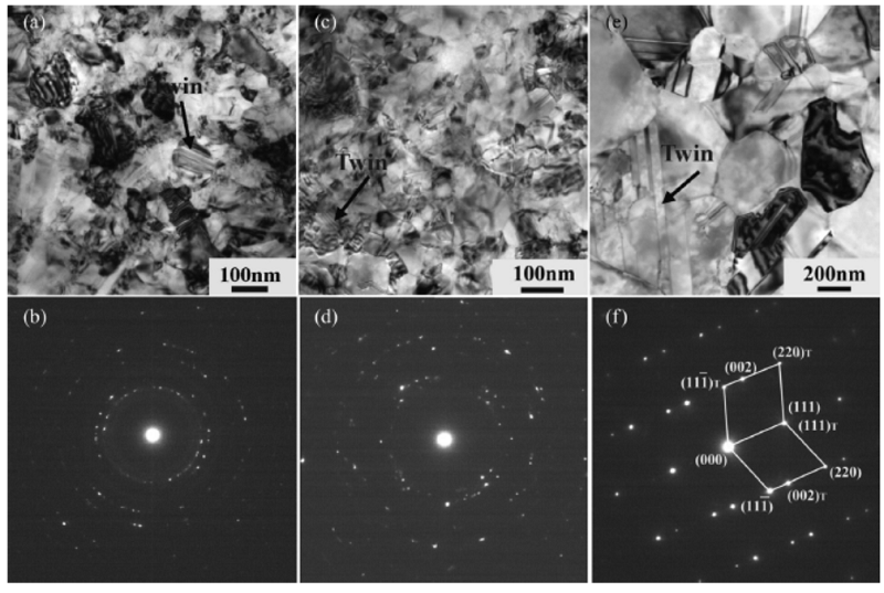
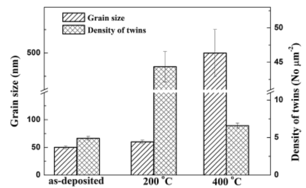
Fig. 1 shows the bright-field TEM images and selected-area diffraction patterns of the nickel coatings. It can be found that the average grain size of the as-deposited specimen is approximately 50 nm (Fig. 1(a)), and that of the specimen after annealing at 200 ° C for 10 min is about 60 nm (Fig. 1(c)), while the specimen after annealing at 400 ° C for 10 min is approximately 500 nm (Fig. 1(e)). The average grain size of the specimen of annealed at 400 ° C is an order of magnitude bigger than those of the as-deposited and annealed at 400 ° C (Fig. 1 and Fig. 2). The diffraction pattern with ring patterns also indicates that the grain size of the as-deposited specimen is almost equal to that of annealing treatment at 200 ° C (Fig. 1(b) and (d)). Furthermore, another marked difference is that the annealing twins can be observed on the specimen after annealing at 200 ° C and 400 ° C, and the density of annealing twins is about 45 number/µ m2 and 8 number/µ m2, respectively (Fig. 2), while a low density of growth twins (about 5 number/µ m2) can be found on the specimen of the as-deposited. The selected-area diffraction patterns of the nickel coatings indicate that both twins are the {111}/[112] type (Fig. 1(f)).
Fig. 1. TEM micrographs and diffraction pattern of the as-deposited specimen (a) and (b); annealed specimen at 200 ° C (c) and (d); annealed specimen at 400 ° C (e) and (f).
Fig. 2. Grain size and twins density of the as-deposited and annealed specimens at various temperatures.
Marion and Cohen[25] suggested that glide dislocations constituting a blocked slip band could dissociate into Frank and Shockley partials, and that the glide of Shockley partials on intersecting {111} planes could result in overlapping intrinsic faults, leading to the formation of twins. Again, twins do not lie on the primary slip plane, and an additional constraint is that glide dislocations must be correctly spaced within the slip band so that the cross-slip of Shockley partials could lead to intrinsic stacking faults on parallel {111} planes. It has been demonstrated that twinning in fcc crystals does not begin until the co-planar slip vector is activated on the primary plane[26].
Crystallographically, annealing and growth twins are identical and composed of stacking faults on consecutive {111} planes. These faults are produced by the glide of Shockley partials. High deposition rate introduced increasing growth stress into nanocrystalline nickel coatings during electrodeposition, which was in favor of formation of growth twins. Generally, twins boundaries possessing a low free energy locate in a {111} plane common to both adjoined grains. For example, the boundary free energy (0.01 J/m2) of a coherent twins is far lower than that (typically 1.0 J/m2) of random boundaries[27].
These results demonstrate that the grain can grow up slowly after annealing at 200 ° C for 10 min while rapidly grow up from nanometers scale to submicrometer after annealing at 400 ° C for 10 min. Both annealed specimens contain annealing twins and the density of annealing twins decreases with the increase of annealing temperature.
3.2. Potentiodynamic polarization curves
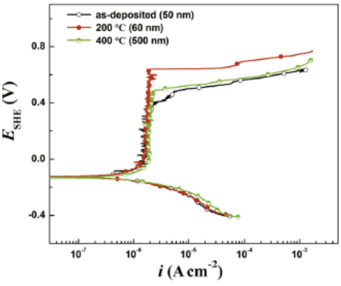
The potentiodynamic polarization curves of the as-deposited and annealed specimens in borate buffer solution are shown in Fig. 3. It can be observed that all the polarization curves show a similar feature in the cathodic part while there is an obvious difference in the anodic region. The as-deposited and annealed specimens show typical self-passivation characteristics. The values of the corrosion current densities, the corrosion potentials and the passivation current densities of three specimens are almost equal, respectively. The pitting potentials (Epit) of annealed specimens greatly shift toward the positive direction in comparison with the as-deposited specimen (0.4 VSHE, 50 nm) and reach up to 0.64 VSHE (60 nm) and 0.49 VSHE (500 nm) after annealing at 200 ° C and 400 ° C, respectively. This has been demonstrated to be related to the adsorption capability of chloride ions on the passive film[24]. And the passive potential zones are apparently broadened correspondingly. Generally, the corrosion current density and the corrosion potential are used to characterize the active dissolution ability of materials, while the passive current density and the pitting potential are used to evaluate the chemical stability and corrosion resistance of passive films[23]. It reveals that the corrosion resistances of annealed specimens remarkably increase in comparison with the as-deposited counterpart, and decrease with the increase of annealing temperature.
Fig. 3. Potentiodynamic polarization curves of the as-deposited and annealed specimens with different microstructures.
These results are consistent with the abnormal grain size effect reported in our last work[24]. But the trends of the pitting potentials are closely related to trends of the twins densities of the coatings (Fig. 2). It is known that grain size and twins structure are both important for enhancing the corrosion resistance of materials. This indicates that there exists a competition between the effects of grain size and twins density on the corrosion resistance of the passive films. And apparently, the effect of twins density on the corrosion resistance of nickel coatings is stronger than that of grain size.
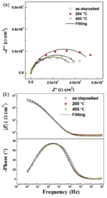
3.3. Electrochemical impedance spectroscopy
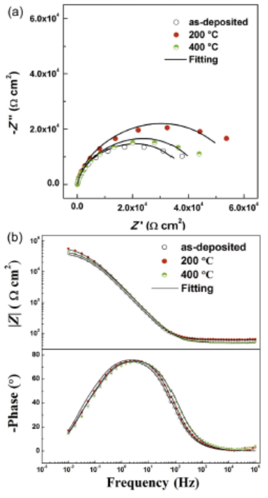
The EIS measurements were carried out at open circuit potential. The Nyquist and Bode plots of the three specimens are shown in Fig. 4. It can be seen that there is a common feature on the Nyquist plots of all specimens (Fig. 4(a)), a single capacitive semicircle existing in the measured frequency range. While the sizes of semicircle of annealed specimens are bigger than that of the as-deposited, and the size of semicircle after annealing at 200 ° C is bigger than that of annealing at 400 ° C. Fig. 4(b) shows the corresponding Bode plots of all specimens. The model value of impedance (|Z|) and the phase value are often used to evaluate the stability of passive film. The bigger the value of |Z| and the nearer to 90° the phase angle, the more stable the passive film is. It can be seen that the value of impedance and phase angle of the specimen after annealing at 200 ° C are the biggest and the as-deposited counterpart are the smallest.
Fig. 4. EIS of the as-deposited and annealed specimens with different microstructures: (a) Nyquist plots, (b) Bode plots. The solid points are experimental data and the solid lines are the fitting results using the equivalent electrical circuit in Fig. 5.
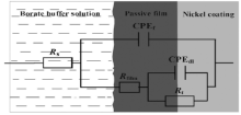
It has been demonstrated that a relatively stable passive film could be self-formed on these three nickel coatings (Fig. 3). There must be ultimately a dynamic equilibrium between the growth and dissolution process of the passive film. Generally, it is agreed that oxide ions migrate from the film/solution interface to the metal/film interface and metal ions migrate in the reverse direction, resulting in the growth of the passive film[28]. Metal ions were formed at metal/film interface by electrochemical reactions. The corrosion rate was controlled by the electrochemical reactions and the ions migration. Based on such interface structure of the passive film on the specimens, an equivalent circuit model (Fig. 5) is proposed to stimulate the interfacial process when the specimens were soaked in the test solution, where Rs is the solution resistance, CPEf is constant phase element (CPE) of the passive film capacitance, Rfilm is the passive film resistance, CPEdl is the double layer capacitance and Rt is the charge transfer resistance, respectively. Such model is also similar to the models proposed by other researchers when they investigated the corrosion behavior of alloys containing nickel [29, 30, 31].
Fig. 5. Equivalent circuit used to simulate the EIS data in Fig. 4.
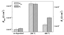
The equivalent circuit in Fig. 5 is used to fit the EIS data in Fig. 4. It can be seen that the fitting is perfect. The fitting results are shown in Fig. 6. It shows that Rfilm increases from 3.0 × 10⁴ Ω cm2 to 4.1 × 10⁴ Ω cm2 and Rt increases from 9.4 × 10³ Ω cm2 to 1.58 × 10⁴ Ω cm2 after annealing at 200 ° C for 10 min compared with the as-deposited counterpart, and the value of Rt and Rfilm of the nickel coating after annealing at 400 ° C is intermediate. Rfilm is an indicator of the resistance to the migration of ions in the passive film and Rt is an indicator of the resistance to the electrochemical reactions (Ni→ Ni2+ + 2e) at metal/film interface. Therefore, there is more resistance to ions migration and electrochemical reactions for the specimen (60 nm) after annealing at 200 ° C. This is completely consistent with the results obtained from potentiodynamic polarization measurements. Furthermore, the value of Rfilm and Rt has the same order of magnitude, indicating that the corrosion process on these specimens is jointly controlled by the resistance of the passive film to the ions migration and the resistance to the electrochemical reactions at metal/film interface.
Fig. 6. Fitting values of Rfilm and Rt of the as-deposited and annealed specimens with different microstructures using the equivalent electrical circuit in Fig. 5.
It has been demonstrated (Fig. 1 and Fig. 2) that the nanocrystalline nickel coatings after annealing at 200 ° C for 10 min not only possesses a large amount of annealing twins compared with that of the as-deposited and that of annealing at 400 ° C, but also the average grain size of coatings remains within the scope of nanocrystalline (60 nm). While the average grain size of the nickel coatings annealing at 400 ° C (500 nm) was much bigger than that of the as-deposited (50 nm) and annealed at 200 ° C (60 nm). Apparently, the trends of Rfilm and Rt are also consistent with the abnormal grain size effect, but are closely related to the trends of twins density, indicating the twins density dominates the corrosion resistance of the coating. The results agree with the report that the twins boundaries possessing a low free energy are always beneficial to improving the corrosion resistance of materials[21]. This is because the higher the twins density, the more homogeneous the distribution of various components across the passive films, and the weaker capability to adsorb chloride ions, leading to the decreasing of its pitting susceptibility[32].
4. Conclusion
Due to the presence of high densities of annealing twins and nanocrystalline structure after annealing at 200 ° C for 10 min, the pitting resistance of the nickel coating was significantly improved. Although the average grain size of the specimen after annealing at 400 ° C rapidly grew up from nanometers to submicrometer scale, the annealing twins density is still higher than that of as-deposited counterpart. Correspondingly, the pitting resistance of the nickel coating after annealing at 400 ° C was more positive than that of the as-deposited counterpart. The results indicate that the twins density and grain size are both important to the corrosion resistance of materials, but the effect of twins density predominates over that of grain size.
AcknowledgementsAcknowledgments
The authors acknowledge the financial support from the National Basic Research Program of China (No. 2014CB643301), the National Natural Science Foundation of China (Nos. 50971050 and 51001036), the Program for New Century Excellent Talents in University (No. NCET-11-0575), the Ministry of Science and Technology of the People's Republic of China (No. 2012FY113000) and the Key Laboratory of Superlight Materials and Surface Technology (Harbin Engineering University, No. HEUCF20151011), Ministry of Education (No. HEUCF20151011).
The authors have declared that no competing interests exist.
U. Klement, U. Erb, A. M. El-Sherik, K. T. Aust, Mater. Sci. Eng. 203(1995) 177-186. [Cited within:1]
[3]
N. Wang, Z. Wang, K. T. Aust, U. Erb, Acta Mater. 45(1997) 1655-1669. [Cited within:1]
[4]
T. Turi, Thermal and thermodynamic properties of fully dense nanocrystalline Ni and Ni-Fe alloys (Ph. D. Thesis), Queen’s University, Canada, 1997. [Cited within:1]
G. D. Hibbard, U. Erb, K. T. Aust, U. Klement, G. Palumbo, Mater. Sci. Forum 386-388(2002) 387-396. [Cited within:2]
[7]
M. Abraham, P. Holdway, M. Thuvand er, A. Cerezo, G. D. W. Smith, Surf. Eng. 18(2002) 151-156. [Cited within:1]
[8]
M. H. Yoo, A. Hishinuma, Met. Mater. Int. 3(1997) 65-74. [Cited within:1]
[9]
B. K. Lee, S. Y. Chung, S. J. L. Kang, Met. Mater. Int. 6(2000) 301-304. [Cited within:1]
[10]
N. H. Cho, C. B. Carter, Met. Mater. Int. 6(2000) 181-187. [Cited within:1]
[11]
H. Y. Kim, J. Matsuda, K. Maruyama, Met. Mater. Int. 9(2003) 255-263. [Cited within:1]
[12]
V. Rand le, The Role of the Coincidence Site Lattice in Grain Boundary ngineering, Cambridge University Press, Cambridge1996, pp. 78-86. [Cited within:1]
[13]
H. Carpenter, S. Tamura, Proc. Roy. Soc. Lond. 113(1926) 161-182. [Cited within:1]
[14]
S. Dash, N. Brown, Acta Metall. 11(1963) 1067-1075. [Cited within:1]
[15]
W. Y. Gertsman, K. Tangri, R. Z. Valiev, Acta Metall. Mater. 42(1994) 1785-1804. [Cited within:1]
L. Lu, Y. Shen, X. Chen, L. Qian, K. Lu, Science304 (2004) 422-426. [Cited within:1]
[19]
K. T. Aust, U. Erb, G. Palumbo, Mater. Sci. Eng. 176(1994) 329-334. [Cited within:1]
[20]
G. Meng, Y. Shao, T. Zhang, Y. Zhang, F. Wang, Electrochim. Acta53 (2008) 5923-5926. [Cited within:1]
[21]
F. Sun, G. Meng, T. Zhang, Y. Shao, F. Wang, C. Dong, X. Li, Electrochim. Acta54(2009) 1578-1583. [Cited within:2]
[22]
L. Liu, Y. Li, F. Wang, Electrochim. Acta53 (2008) 2453-2462. [Cited within:1]
[23]
G. Meng, Y. Li, F. Wang, Electrochim. Acta51 (2006) 4277-4284. [Cited within:2]
[24]
G. Meng, Y. Li, Y. Shao, T. Zhang, Y. Wang, F. Wang, X. Cheng, C. Dong, X. Li, J. Mater. Sci. Technol. 31(2015) 1186-1192. [Cited within:3]
[25]
R. H. Marion, J. B. Cohen, J. Appl. Cryst. 8(1975) 430-435. [Cited within:1]
[26]
C. S. Pand e, P. M. Hazzledine, Philos. Mag. A24 (1971) 1039-1057. [Cited within:1]
[27]
U. Wolf, F. Emst, T. Muschik, M. W. Finnis, H. F. Fischmeister, Philos. Mag. A 66(1992) 991-1016. [Cited within:1]
[28]
D. D. Macdonald, J. Electrochem. Soc. 139(1992) 3434-3449. [Cited within:1]
[29]
J. Pan, G. Leygraf, R. F. Jargelius, J. Linden, Oxid. Met. 50(1998) 431-455. [Cited within:1]
[30]
A. L. Rudd, C. B. Breslin, F. Mansfeld, Corros. Sci. 42(2000) 275-288. [Cited within:1]
[31]
P. Girault, J. L. Grosseau-Poussard, J. F. Dinhut, L. Marechal, Nucl. Instrum. Meth. Phys. Res. B174 (2001) 439-452. [Cited within:1]
[32]
G. Meng, F. Sun, Y. Shao, T. Zhang, F. Wang, Electrochim. Acta55 (2010) 2575-2581. [Cited within:1]
1
0.0
0.0
... IntroductionRecently, nanocrystalline materials have attracted much attention due to their unique microstructure with a large number of interfaces and their novel properties different from that of conventional coarse-grained counterparts[1] ...
1
0.0
0.0
... A common finding in the thermal stability studies on electrodeposited nanocrystalline nickel is the significantly increased rate of grain growth at relatively low temperatures[2, 3, 4, 5, 6] ...
1
0.0
0.0
... A common finding in the thermal stability studies on electrodeposited nanocrystalline nickel is the significantly increased rate of grain growth at relatively low temperatures[2, 3, 4, 5, 6] ...
1
1997
0.0
0.0
... A common finding in the thermal stability studies on electrodeposited nanocrystalline nickel is the significantly increased rate of grain growth at relatively low temperatures[2, 3, 4, 5, 6] ...
2
0.0
0.0
... A common finding in the thermal stability studies on electrodeposited nanocrystalline nickel is the significantly increased rate of grain growth at relatively low temperatures[2, 3, 4, 5, 6] ...
... [5, 6] have reported that nanocrystalline nickel was sufficient to completely consume the as-deposited matrix by abnormal grain growth after annealing for 30 min at 593 K and for 30 s at 693 K ...
1
0.0
0.0
... [7] found that the electrodeposited nanocrystalline nickel annealed at 250 #cod#x000b0 ...
1
0.0
0.0
... In certain fcc metals and alloys of low stacking fault energy, annealing twins are easy to form during annealing treatment[8, 9, 10, 11, 12] ...
1
0.0
0.0
... In certain fcc metals and alloys of low stacking fault energy, annealing twins are easy to form during annealing treatment[8, 9, 10, 11, 12] ...
1
0.0
0.0
... In certain fcc metals and alloys of low stacking fault energy, annealing twins are easy to form during annealing treatment[8, 9, 10, 11, 12] ...
1
0.0
0.0
... In certain fcc metals and alloys of low stacking fault energy, annealing twins are easy to form during annealing treatment[8, 9, 10, 11, 12] ...
1
1996
0.0
0.0
... In certain fcc metals and alloys of low stacking fault energy, annealing twins are easy to form during annealing treatment[8, 9, 10, 11, 12] ...
1
0.0
0.0
... Annealing twins were first observed by Carpenter and Tamura over 80 years ago[13] ...
1
0.0
0.0
... In 1963, Dash and Brown[14] made pioneering observations on the early stages of annealing twins ...
1
0.0
0.0
... [15] pronounced that the evolving grain boundary distribution could only be due to a result of evolving multiple annealing twins ...
1
0.0
0.0
... The formation of twins structure can contribute to the resultant mechanical, physical or chemical properties[16, 17] ...
1
0.0
0.0
... The formation of twins structure can contribute to the resultant mechanical, physical or chemical properties[16, 17] ...
1
2004
0.0
0.0
... [18] demonstrated that the mechanical and electrical properties of coatings with twins structure were remarkably enhanced compared with the conventional crystalline and nanocrystalline counterparts as well ...
1
0.0
0.0
... The enhanced intergranular fracture and corrosion resistance of materials were also associated with the twins boundaries[19] ...
1
2008
0.0
0.0
... In our previous work, the corrosion behaviors of nanocrystalline nickel coatings with twins structure were studied, indicating that the twins structure was in favor of the enhancement of the corrosion resistance[20, 21] ...
2
2009
0.0
0.0
... In our previous work, the corrosion behaviors of nanocrystalline nickel coatings with twins structure were studied, indicating that the twins structure was in favor of the enhancement of the corrosion resistance[20, 21] ...
... The results agree with the report that the twins boundaries possessing a low free energy are always beneficial to improving the corrosion resistance of materials[21] ...
1
2008
0.0
0.0
... [22] investigated the effects of grain size on the electrochemical corrosion behavior of a Ni-based superalloy nanocrystalline coating fabricated by a magnetron sputtering technique and found that the smaller the grain size, the less the amount of chloride ions adsorbed on the surface, which promoted the formation of compact passive film, and significantly increased the resistance to pitting corrosion ...
2
2006
0.0
0.0
... [23] studied the corrosion behavior of nanocrystalline Fe-10Cr coating and found that the chemical stability of the passive film was significantly improved compared with the conventional counterpart ...
... Generally, the corrosion current density and the corrosion potential are used to characterize the active dissolution ability of materials, while the passive current density and the pitting potential are used to evaluate the chemical stability and corrosion resistance of passive films[23] ...
3
0.0
0.0
... However, our last work[24] showed an abnormal grain size effect on the corrosion resistance of nickel coating ...
... This has been demonstrated to be related to the adsorption capability of chloride ions on the passive film[24] ...
... These results are consistent with the abnormal grain size effect reported in our last work[24] ...
1
0.0
0.0
... Marion and Cohen[25] suggested that glide dislocations constituting a blocked slip band could dissociate into Frank and Shockley partials, and that the glide of Shockley partials on intersecting {111} planes could result in overlapping intrinsic faults, leading to the formation of twins ...
1
1971
0.0
0.0
... It has been demonstrated that twinning in fcc crystals does not begin until the co-planar slip vector is activated on the primary plane[26] ...
1
1992
0.0
0.0
... 0 J/m2) of random boundaries[27] ...
1
0.0
0.0
... Generally, it is agreed that oxide ions migrate from the film/solution interface to the metal/film interface and metal ions migrate in the reverse direction, resulting in the growth of the passive film[28] ...
1
0.0
0.0
... Such model is also similar to the models proposed by other researchers when they investigated the corrosion behavior of alloys containing nickel [29, 30, 31] ...
1
0.0
0.0
... Such model is also similar to the models proposed by other researchers when they investigated the corrosion behavior of alloys containing nickel [29, 30, 31] ...
1
2001
0.0
0.0
... Such model is also similar to the models proposed by other researchers when they investigated the corrosion behavior of alloys containing nickel [29, 30, 31] ...
1
2010
0.0
0.0
... This is because the higher the twins density, the more homogeneous the distribution of various components across the passive films, and the weaker capability to adsorb chloride ions, leading to the decreasing of its pitting susceptibility[32] ...
Effect of Microstructures on Corrosion Behavior of Nickel Coatings: (II) Competitive Effect of Grain Size and Twins Density on Corrosion Behavior
[Guozhe Meng1,2,*, Yang Li1, Yawei Shao1,2, Tao Zhang1,2, Yanqiu Wang1, Fuhui Wang1,2, Xuequn Cheng3, Chaofang Dong3, Xiaogang Li2,3]


 , Yang Li