Microstructure of Electrodeposited Cu Micro-cylinders in High-Aspect-Ratio Blind Holes and Crystallographic Texture of the Cu Overburden Film
Cite this Article
Yazhou Zhang, Guifu Ding, Hong Wang, Ping Cheng. Microstructure of Electrodeposited Cu Micro-cylinders in High-Aspect-Ratio Blind Holes and Crystallographic Texture of the Cu Overburden Film. Journal of Materials Science & Technology, 2016, 32(4): 355-361 
Permissions
Copyright reserved, Editorial board of Journal of Materials Science & Technology
Microstructure of Electrodeposited Cu Micro-cylinders in High-Aspect-Ratio Blind Holes and Crystallographic Texture of the Cu Overburden Film
Abstract
Microstructure and texture of electrodeposited Cu micro-cylinders in the blind hole play a vitally important role in the electrical and mechanical properties of the three-dimensional (3-D) IC (integrated circuit)/Si integrations. In this paper, a new commercial additive system, which is specifically developed for the high-aspect-ratio through-silicon-via (TSV) filling, was used to electrodeposit Cu in the blind holes. The microstructure of electrodeposited Cu micro-cylinder in the blind hole with a diameter of 40 µm and a depth of 140 µm was investigated by electron back-scattered diffraction (EBSD) technique. Grain size distribution of the Cu micro-cylinder in the blind hole differed from the bottom to the top. The grain boundaries contained a high fraction of Σ3 CSL (coincident site lattice) boundaries. It has been reported that the Cu overburden film on the surface of the blind hole influenced the crystallographic orientation of Cu grains inside the damascene trench. So the effects of the current density and additive concentration on the crystal structure of the overburden Cu film were also studied in this study. The experimental results indicated that the preferred orientation of the Cu overburden film changed from {111} to {220} when the current density increased from 2 to 80 mA cm-2. However, the effect of additives on the crystal structure of the Cu overburden film was dependent on the crystal structure of the seed layer.
Keyword:
Cu micro-cylinder electrodeposition; Electron back-scattered diffraction (EBSD); Crystallographic orientation; Cu overburden film
1. Introduction
Three-dimensional (3D) packaging has been reported to be an effective approach to prolong Moore's law, which is based on the interconnection of devices in a multilayer laminated structure[1 , 2]. Through-silicon-via (TSV) technology is considered as the heart of 3D IC (integrated circuit)/Si integrations, which provides the shortest vertical interconnections with a large number of significant advantages[1 , 2]. The TSV technology contains several processes, such as etching holes in the Si chip, depositing the insulating layer/barrier layer/seed layer, filling the Cu conductor in the blind holes, removing the backside Si and the Cu overburden film by chemical mechanical polishing to expose the Cu micro-cylinder, and ball bonding process. Copper electrodeposition has received extensive investigation due to its excellent electrical conductivity, low electromigration, and relatively mature electrodeposition process[3 , 4]. It becomes a dominant technology to fabricate interconnecting conductors by filling submicron damascene trenches and blind holes of TSV technology[5]. The Cu electric conductors without any voids are ideal for TSV technology to ensure their mechanical and electrical performances. To achieve void-free electrodeposited Cu, some additives are specially developed to obtain bottom-up Cu filling mode in the high-aspect-ratio blind holes. The most widely used additives are chloride ions (Cl-), accelerator (bis(3-sulfopropyl)disulfide, SPS), suppressor (poly(ethylene glycol), PEG), and leveler (Janus green B, JGB)[5, 6, 7 , 8]. The use of additives will bring some side effects, including incorporation of impurities into the deposits. It may cause defects between grain boundaries, which would affect its secondary recrystallization at room temperature[4, 9, 10, 11 , 12]. Besides, the use of additives in plating bath might change the preferred orientation of deposits dramatically[4, 11 , 13].
The preferred orientation (texture) has an influence on the material's electrical conductivity, electromigration resistance, hardness, magnetic penetrance, chemical activity, etc[11, 14, 15, 16]. It has been reported that the (111) texture is ideal for the electronic applications (high electromigration resistance and high electrical conductivity)[9 , 15]. In damascene trenches, the electrodeposited Cu in the trench do not fully recrystallize at room temperature if the Cu overburden film on the upper surface of the trenches is removed by chemical mechanical polishing (CMP). The Cu overburden film influences the crystallographic orientation of Cu inside the damascene trench due to the topographic environment for Cu recrystallization in the narrow submicron trench[10].
In the electrodeposition process, the formation of texture depends on the nature of deposited metal, current density, seed layer, electrolyte composition (base electrolyte, additives and pH value), and temperature[7, 11, 13, 14, 15 , 17]. Additives play an important role in forming the void-free Cu micro-cylinders in high-aspect-ratio blind holes. They adsorb on the surface of deposits, which would change the mechanism of Cu electrodeposition. Some researchers have demonstrated the effect of additives on the copper electrodeposition using in-situ scanning tunneling microscopy (STM) and atomic force microscopy (AFM) technique[5, 18 , 19]. However, they used solid planar cathode without any blind holes for electrodeposition, which cannot completely simulate the electrodeposition process of Cu in the high-aspect-ratio blind holes since the diffusion of cupric ions, additives and by-products in the high-aspect-ratio blind holes is not considered.
For TSV technology, the dimension of blind holes is 100 times larger than that of the submicron damascene trench[20 , 21], so the diffusion of cupric ions, additives and by-products in the high-aspect-ratio blind holes is much more difficult than that in the damascene trench. It would lead to the different Cu electrodeposition condition, thus different microstructures of Cu micro-cylinders compared to the electrodeposited Cu in damascene trench.
In the last several decades, many researchers have studied the microstructure and texture of electrodeposited Cu in the submicron damascene trenches and Cu films on the solid planar cathode without any holes[4, 10, 11, 12, 15 , 22]. However, few researchers have reported the microstructure of Cu micro-cylinders electrodeposited in high-aspect-ratio blind holes and crystallographic texture of the Cu overburden film electroplated in the bath containing new commercial additive systems specifically developed for filling the high-aspect-ratio blind holes. Considering the effects of the electrodeposition condition and the Cu overburden film on the microstructures of Cu micro-cylinders, it is vitally necessary to study the microstructures of Cu electrodeposited in blind holes and of the Cu overburden film.
In this paper, a new commercial additive system (MICROFAB DVF 200, Enthone Inc.) specifically developed for filling the high-aspect-ratio blind holes was used for Cu electrodeposition. The silicon wafer containing an array of blind holes, which was covered by an insulting layer, a barrier layer and a seed layer, was used as cathode. The microstructures of electrodeposited Cu micro-cylinders in blind holes and Cu overburden film were characterized by scanning electron microscopy (SEM), electron back-scattered diffraction (EBSD) and X-ray diffraction (XRD) techniques, respectively. The effects of the current density, the additive concentration and seed layer on the crystal structure of the electrodeposited Cu overburden film were investigated.
2. Materials and Methods
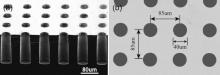
The base electrolyte contained 80 g L-1 Cu(CH3SO3)2, 20 g L-1 CH3SO3H and 50 mg L-1 HCl. A new commercial additive system (MICROFAB DVF 200, DVF-B, DVF-C and DVF-D, Enthone Inc.) specifically developed for filling high-aspect-ratio blind holes was used in the electroplating experiment. DVF-B, DVF-C, and DVF-D correspond to accelerator, suppressor, and leveler, respectively. For convenience, they are briefly referred to as A, S, and L, respectively. A phosphorus-containing copper slice was utilized as anode. Firstly, the silicon wafer containing an array of blind holes was thermally oxidized to form an SiO2 insulating layer. Then, the Ti barrier layer and Cu seed layer were sputtered sequentially on the thermal-oxide SiO2 layer. Finally, the Si wafer mentioned above was cut into 10 mm × 10 mm square chips as cathode for the following electrodepositing experiments. As shown in Fig. 1, the dimension of the blind via is 40 µ m in diameter and 140 µ m in depth. The center to center distance between the adjacent vias is ca. 85 µ m.
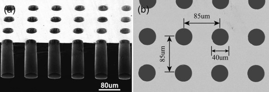 | Fig. 1. SEM images of the via dimension and the arrays of the blind holes: (a) cross-sectional SEM micrograph of the blind holes, (b) top view of an array of the blind holes. |
XRD technique (Bruker-axs, D8 Advance) was conducted to analyze the crystal structure of the electrodeposited Cu overburden films. The Cu-filled blind holes were cross-sectioned by an ion polishing equipment (Gatan Ilion+, Gatan Inc.). The microstructure of cross-sectioned Cu micro-cylinder was characterized using EBSD (AZTec HKL Max) technique. The CHANNEL 5 software (HKL technology, Oxford Instruments) was used to analyze the microstructure of the Cu micro-cylinder.
3. Results and Discussion
3.1. Microstructures of Cu micro-cylinder
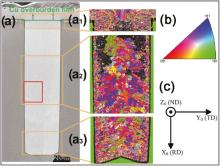
4 ppm DVF-B, 20 ppm DVF-C and 1.5 ppm DVF-D were added in the base electrolyte for Cu electrodeposition in the blind holes (Ø 40 µ m × 140 µ m) at room temperature. The applied direct current (DC) density was 3 mA cm-2 for 10 min plus 10 mA cm-2 for 270 min. Fig. 2(a) shows the SEM image of the cross-sectional Cu micro-cylinder including the overburden Cu film. The Cu overburden film and Cu micro-cylinder were separated with a green solid line.
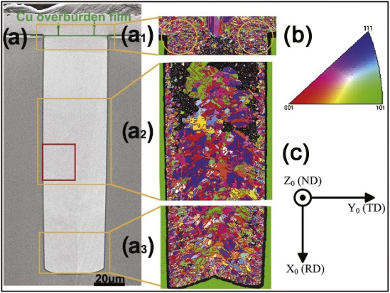 | Fig. 2. EBSD grain map of the cross-sectional Cu micro-cylinder with CSL-GBs. (a) SEM image of the cross-sectional Cu micro-cylinder, and the corresponding EBSD grain maps (a1) in the top region, (a2) in the middle region, and (a3) in the bottom region. (b) Color key. (c) Coordinate system. |
Fig. 2(a1-a3) show the EBSD grain maps with coincidence site lattice-grain boundaries (CSL-GBs) in the top, middle and bottom regions of the cross-sectional Cu micro-cylinder, respectively. As shown in Fig. 2(a1), the grain of electrodeposited Cu in the overburden film is bigger than that in the top region of the Cu micro-cylinder.
Fig. 2(a3) shows the EBSD grain map in the bottom region of the Cu micro-cylinder. It can be seen that grains in this region have an average size of about 1.67 µ m. For the middle region of the Cu micro-cylinder (Fig. 2(a2)), the grains in the lower half have an average size of 1.92 µ m, while some grains in the upper half are so small that their Kikuchi patterns cannot be obtained[23]. These features are very reproducible. The reason for this phenomenon is probably due to the factor that the concentrated suppressors (DVF-C) inhibit Cu grain growth in the upper part of the blind holes[24].
Compared to the Cu damascene, the grain size distribution of Cu micro-cylinder is not uniform from the bottom to the top due to the different concentration distributions of the additives in the high-aspect-ratio holes. Considering the high-aspect-ratio of the blind holes and the long electroplating time, it requires a very large consumption of cupric ions and additives, and produces a large amount of by-products at the deposit surface. The by-products at the bottom of the hole cannot diffuse out timely, so they are incorporated into the deposits. The interaction of additives and their by-products at the deposit surface during the hole filling process leads to defects, dislocations, and incorporation of impurities, which might drive or retard the recrystallization process[4, 11, 12, 22 , 25].
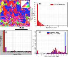
Fig. 3(a) shows the grain map with CSL-GBs of the local region in the middle of the Cu micro-cylinder as indicated by the red solid rectangle in Fig. 2(a). It can be seen that the grain size near the sidewall of the Cu micro-cylinder is smaller than that far from the sidewall. The grain size increases along the growth direction. Besides, many large grains with {111} preferred orientation distribute far from the sidewall. Fig. 3(b) shows the grain size distribution of the Cu deposits. It can be seen that the grain size concentrates in the range of 0-2 µ m.
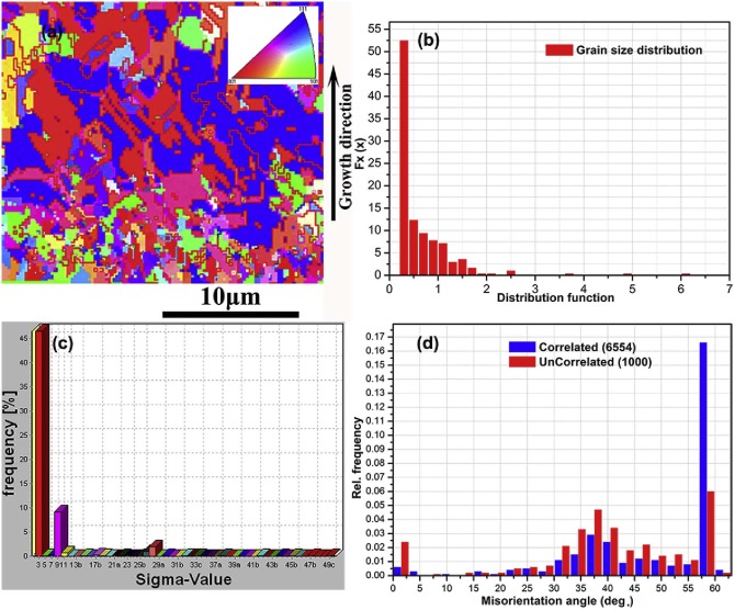 | Fig. 3. (a) EBSD grain map with CSL-GBs of the local region of Cu micro-cylinder, as indicated by a red solid rectangle in Fig. 2(a); (b) grain size distribution; (c) CSL boundary distribution; (d) GB misorientation distribution. |
As shown in Fig. 3(c), it contains the highest fraction of Σ 3 CSL boundaries. The Σ 3 CSL boundary has the lower grain boundary energy than the random high-angle boundary, which is more likely to weaken the electron scattering[23]. Besides, there exists a fraction of Σ 9, Σ 27b and Σ 25b boundaries. The presence of twin boundaries may enhance the tensile strength of the Cu micro-cylinder without losing its high electrical conductivity[26].
The grain boundary distribution of Cu deposits in terms of misorientation angles is shown in Fig. 3(d). It can be seen that grain boundaries with misorientation of 55° -60° occupy the largest fraction, indicating that a large amount of Σ 3 boundaries separate two neighboring grains which is rotated by 60° around the < 111 > axis. Besides, there are a large number of grain boundaries with misorientation of 35° -40° indicating the existence of Σ 9 boundaries, where the grains are rotated by 38.94° around the < 110 > axis.
3.2. Effect of current density on the crystal structure and morphology of the Cu overburden film
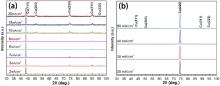
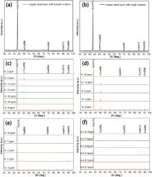
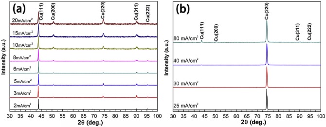
In this section, 11 ppm A, 14 ppm S, and 10 ppm L were added in the base plating electrolyte (80 g L-1 Cu(CH3SO3)2, 20 g L-1 CH3SO3H and 50 mg L-1 HCl). The silicon wafer contains an array of blind holes. The thickness of each Cu overburden film is about 38 µ m. Fig. 4 shows XRD spectra of the Cu overburden film at different current densities (from 2 to 80 mA cm-2). As shown in Fig. 4(a), when the current density of 2 mA cm-2 is applied, the Cu overburden film shows a strong {111} preferred orientation. An increase in the current density increases the intensities of the {200}, {220} and {311} peaks. There exists a sharp change in the diffraction spectra when the applied current density further increases up to 25 mA cm-2. As shown in Fig. 4(b), no other peak appears except the strong {220} preferred orientation when the applied current density is above 25 mA cm-2.
 | Fig. 4. X-ray diffraction spectra of electrodeposited Cu overburden films at different current densities: (a) from 2 to 20 mA cm-2; (b) from 25 to 80 mA cm-2. |
The results mentioned above can be explained as follows. Pangarov[27 , 28] and Kremmer et al.[29] linked the preferred orientation of deposits with the energy needed for the formation of two-dimensional nuclei Whkl, which was regarded as a function of the over-voltage η .
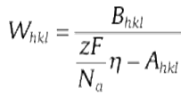 |
where Ahkl and Bhkl are materials parameters that depend on the crystallographic direction < hkl > . z is the number of electrons, Na is the Avogadro constant and F is the Faraday constant. For fcc metals, W111 < W100 < W110 are yielded at a low over-voltage according to Eq. (1), while W110 < W100 < W111 at a high over-voltage η [27], [28] and [29]. The crystallites of the electrodeposited metal have a preferred orientation when the formation energy of a particular nucleus is lower than that of all the other types of nuclei. At the small current density (< 8 mA cm-2), the energy W111 for the formation of two-dimensional {111} orientation nuclei is the smallest one (W111 < W100 < W110) and the Cu overburden film shows {111} preferred orientation. With the increase in the current density (20-40 mA cm-2), {110} oriented nuclei have the least formation energy so that the preferred orientation of Cu overburden films changes from {111} to {220} at high current density.
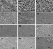
The effect of current density on the morphology of Cu overburden films is also investigated. It can be seen from Fig. 5 that a wide variation in morphological features is obtained. An increase in the current density decreases the crystallite size of the Cu overburden film. The spherical crystallites are observed when the current density is in the range of 8-20 mA cm-2, while the flocci or needle-like crystallites appear when the current density is in the range of 25-80 mA cm-2. Besides, some nodules with a diameter of 100-300 µ m appear on the smooth surface when the current density is 80 mA cm-2, as shown in the insert image of Fig. 5(l). It is found that the nodules always appear when only additive S is used in the electrolyte at the high current density, although the formation mechanism is not clear yet. When the nodule exists near the hole opening, it might seal the hole opening before the blind hole is completely filled. Fortunately, according to our experiments, nodules disappear when another two kinds of additives are added in the electrolyte.
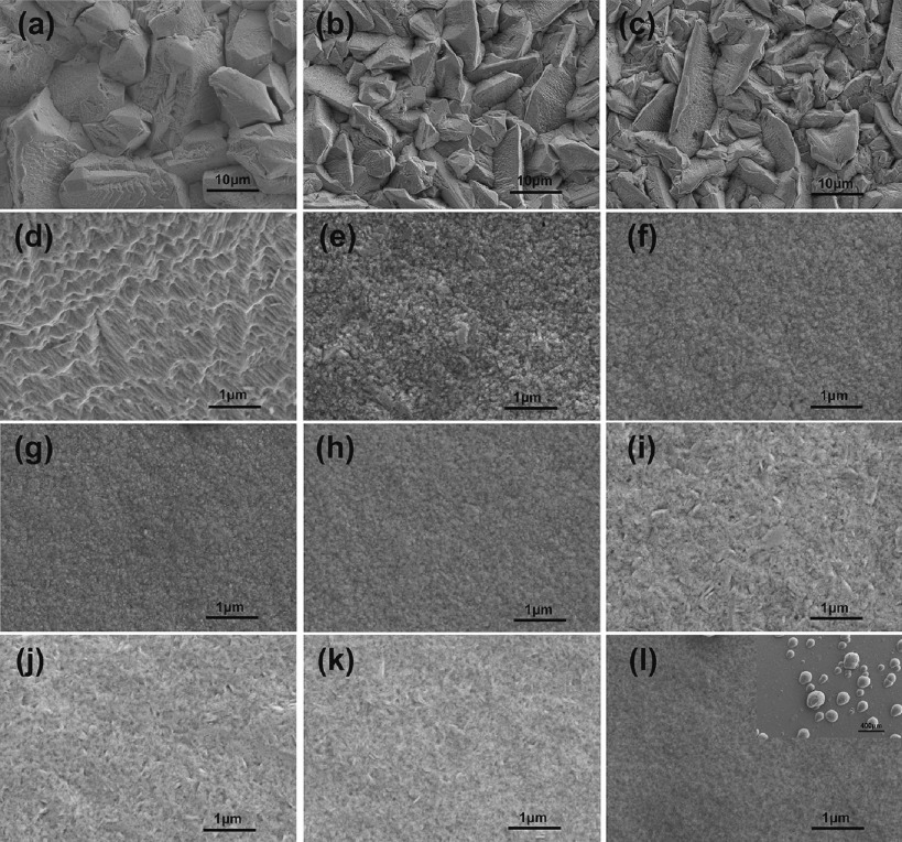 | Fig. 5. SEM images of electrodeposited Cu overburden films at different current densities: (a) 2, (b) 3, (c) 5, (d) 6, (e) 8, (f) 10, (g) 15, (h) 20, (i) 25, (j) 30, (k) 40, and (l) 80 mA cm-2 in Fig. 3. |
Changes in the grain size of the Cu overburden film are related to the electrodeposition mechanism, which can be explained by the model of nucleation and crystal growth. According to the principles of electrocrystallization, the formation rate of new nuclei on the electrode surface increases exponentially as the cathodic polarization η increases [30]:
 |
where T and B are temperature and the constant, respectively, ω is the rate of nuclei formation, and η is the cathodic polarization potential. At the low current density (low cathodic polarization potential), limited nuclei are formed and the grains tend to grow from the existing nuclei, so the large size grains are obtained. An increase in the current density enhances the polarization effect, which promotes the copper nucleation. Massive nuclei cause the formation of fine grains (the crystallite size decreases with increasing cathodic polarization).
3.3. Effect of the seed layer and additives on the crystal orientation of the Cu overburden film
Two kinds of seed layers are used for electrodepositing the Cu overburden film. XRD patterns of #1 and #2 seed layers are shown in Fig. 6(a, b). The #1 seed layer shows very strong {111} preferred orientation. The #2 seed layer also shows {111} preferred orientation, but the intensity of {200} diffraction peak enhances compared to that of the #1 seed layer.
In this section, the thicknesses of each Cu overburden film shown in Fig. 6(c-f) are around 45, 43, 39 and 42 µ m, respectively. All of the current densities used for copper electroplating are 10 mA cm-2. Fig. 6(c, d) shows XRD patterns of Cu overburden films electroplated on the #2 seed layer in the electrolyte containing 0-40 ppm A and 2-20 ppm S, respectively. For quantifying the preferred orientation, the texture coefficient is introduced. The texture coefficient Mhkl of an (hkl) plane is defined by Barrett and Massalski [31] as follows:
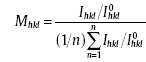 |


From Fig. 6(c), it can be calculated that by increasing the accelerator from 2 to 40 ppm, the {111} texture coefficient increases from 1.39 to 2.39, and the {200} texture coefficient decreases from 1.50 to 0.54, which demonstrates that the accelerators absorb on the deposit surface and induce certain preferred orientations during the electroplating process. As shown in Fig. 6(d), both the {111} preferred orientation and the {200} preferred orientation almost have no change with an increase in the suppressor concentration in the electrolyte. It indicates that the suppressor has little effect on the crystal orientation of the Cu overburden film when the #2 seed layer is used in the electrodeposition process.
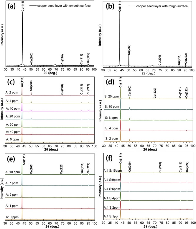 | Fig. 6. X-ray diffraction spectra of electrodeposited Cu overburden films on the different seed layer in the different electrolytes: (a) Cu seed layer #1 with a strong {111} preferred orientation; (b) Cu seed layer #2 with both {111} and {200} preferred orientations; (c) electrodeposited Cu overburden film on the #2 seed layer in the electrolyte containing different contents of the accelerator; (d) electrodeposited Cu overburden film on the #2 seed layer in the electrolyte containing different contents of the suppressor; (e) electrodeposited Cu overburden film on the #1 seed layer in the electrolyte containing different contents of the accelerator; (f) electrodeposited Cu overburden film on the #1 seed layer in the electrolyte containing 4 ppm accelerator and different contents of the suppressor. |
Fig. 6(e, f) shows the XRD patterns of the Cu overburden films electroplated on the #1 seed layer in the electrolyte containing the 0-10 ppm accelerator and 1-15 ppm suppressor in the presence of the 4 ppm accelerator, respectively. It can be seen from Fig. 6(e, f) that they all show strong {111} preferred orientation. Both the concentrations of the accelerator and the suppressor have little effect on the crystal orientation of the Cu overburden film when the seed layer with a very strong {111} preferred orientation is used. In addition to the seed layer with a strong {111} preferred orientation, the smallest energy needed for the formation of two-dimensional {111} orientation nuclei at the small current density also plays an important role in the formation of strong {111} preferred orientation for the Cu overburden film.
According to the experimental results in Fig. 6, it can be concluded that the crystal orientation of the electrodeposited Cu overburden film is influenced not only by the additives but also by the substrate. When the Cu electrodeposition occurs on a single-crystal or on a polycrystalline substrate with a strong preferred orientation, additives adsorbed on the deposit surface have little influence on the crystal orientation of Cu deposits. The preferred orientation of the grains is epitaxially influenced by the crystal structure of the substrate, which corresponds to the case for the #1 seed layer with a strong {111} preferred orientation. However, when the Cu electrodeposition occurs on an inert substrate, the epitaxial influence of the substrate can be ignored. The additives adsorbed on the Cu deposit surface influence the electrodeposition process dramatically. The crystal structure of the Cu overburden film is determined by the electrocrystallization conditions, which correspond to the case for the #2 seed layer.
4. Conclusions
In this paper, a new commercial additive system specifically developed for filling the high-aspect-ratio blind holes was used for Cu electrodeposition. The microstructure of the Cu micro-cylinders including the Cu overburden film was characterized by EBSD technique. The grain size distribution of the Cu micro-cylinder was not uniform from the bottom to the top due to the different concentration distributions of additives in the high-aspect-ratio blind holes. The grain size in the bottom and in the middle of the Cu micro-cylinder was bigger than that in the top. The grain size near the sidewall of the blind hole was smaller than that far from the sidewall. The grain boundaries of the Cu micro-cylinder contain the highest fraction of Σ 3 CSL boundaries. Besides, there were a large number of grain boundaries with misorientation between 35° and 40° .
An increase in the current density from 2 to 80 mA cm-2 changed the preferred orientation of the Cu overburden film from {111} to {220}. The grain growth from the existing nuclei was favored at the low current density (< 8 mA cm-2), while massive nucleation was predominant at the high current density (> 20 mA cm-2), which gave rise to small Cu grains. When the Cu electrodeposition took place on an inert seed layer, the accelerator affected the preferred orientation of Cu deposits dramatically. But when the seed layer with a very strong {111} preferred orientation was used as cathode, both the accelerator and the suppressor had little effect on the crystal orientation of the Cu overburden film.
This work is sponsored by Chinese National Science and Technology Major Project (No. 2011ZX02702-003). We also thank Mahreen for providing language help.
The authors have declared that no competing interests exist.
Reference
| [1] |
|
| [2] |
|
| [3] |
|
| [4] |
|
| [5] |
|
| [6] |
|
| [7] |
|
| [8] |
|
| [9] |
|
| [10] |
|
| [11] |
|
| [12] |
|
| [13] |
|
| [14] |
|
| [15] |
|
| [16] |
|
| [17] |
|
| [18] |
|
| [19] |
|
| [20] |
|
| [21] |
|
| [22] |
|
| [23] |
|
| [24] |
|
| [25] |
|
| [26] |
|
| [27] |
|
| [28] |
|
| [29] |
|
| [30] |
|
| [31] |
|
| [32] |
|