... Over the past two decades, various compositions of chemical bath have been used to deposit CBD-ZnS thin films, such as zinc salt/NH3/SC(NH2)2[7,16,18,19,20,21,22,23], ZnCl2/NH4NO3/SC(NH2)2/KOH[24], zinc salt/NH3/(NH2)2/SC(NH2)2[25,26,27,28,29,30,31,32,33,34,35,36,37,38] (the compositions consist of the addition of complementary agents), ZnCl2/NH3/HONH3Cl/SC(NH2)2[39], ZnCl2/NH3/C6H15NO3 (triethanolamine, TEA)/SC(NH2)2[40], ZnCl2/urea/CH3CSNH2 (thioacetamide, TAA)/HCl[41], Zn(CH3COO)2/NH3/(NH2)2/COOH(CHOH)2COOH/SC(NH2)2[42], Zn(CH3COO)2/Na3C6H5O7/SC(NH2)2[43], Zn(CH3COO)2/C6H15NO3/Na3C6H5O7/SC(NH2)2/NH3/NH4Cl[44,45], ZnSO4/CH3CS-NH2[46], Zn(CH3COO)2 or ZnSO4/Na3C6H5O7/SC(NH2)2/NH3[47,48,49,50,51,52,53,54], ZnCl2/N(CH2CO-OH)3 (nitrilotriacetic acid, NTA)/CH3CSNH2/NaOH[55], Zn(CH3COO)2/COOH-(CHOH)2COOH/Na3C6H5O7/SC(NH2)2/NH3[56], Zn(CH3COO)2/H2NCH2CH2NH2 (ethylenediamine, En)/CH3CSNH2/HCl[57], ZnSO4/CH3CSNH2/HCl/CH3COOH[58], Zn(CH3COO)2/C10H14N2O8Na2 (tetra-acetate disodium salt, Na2EDTA)/CH3CSNH2/NaOH[59], Zn(CH3COO)2/C10H14N2O8Na2 or EDTA/Na3C6H5O7/SC(NH2)2/NH4OH[8,60], Zn(CH3COO)2/CH3CSNH2/C10H14N2O8Na2/C6H12N4 (hexamethylenetetramine, HMTA)/HCl[61], ZnSO4/NH3/CH3CSNH2[62], zinc salts (different zinc salts: Zn(CH3COO)2, ZnSO4, ZnCl2, or Zn(NO3)2)/urea/CH3CSNH2/NaOH/HCl[63], and so on ...
... At the same time, many variables, such as concentrations of various reagents[22,24,25,32,33], pH values[28,29,31,34,61,63], complexing agents[25,40,42,43,49,56,59,64], deposition temperature[21,35,57,65] and time[35,36], annealing treatment[21,27,42,59], stirring speeds[7,25,35,55,66], and substrates[39,57], co-deposition of alloy compounds[26,37,52,67], ammonium salts or buffer solutions[28,32,38] have been investigated ...
... At the same time, many variables, such as concentrations of various reagents[22,24,25,32,33], pH values[28,29,31,34,61,63], complexing agents[25,40,42,43,49,56,59,64], deposition temperature[21,35,57,65] and time[35,36], annealing treatment[21,27,42,59], stirring speeds[7,25,35,55,66], and substrates[39,57], co-deposition of alloy compounds[26,37,52,67], ammonium salts or buffer solutions[28,32,38] have been investigated ...
... At the same time, many variables, such as concentrations of various reagents[22,24,25,32,33], pH values[28,29,31,34,61,63], complexing agents[25,40,42,43,49,56,59,64], deposition temperature[21,35,57,65] and time[35,36], annealing treatment[21,27,42,59], stirring speeds[7,25,35,55,66], and substrates[39,57], co-deposition of alloy compounds[26,37,52,67], ammonium salts or buffer solutions[28,32,38] have been investigated ...
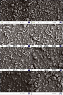
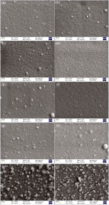
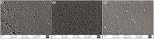
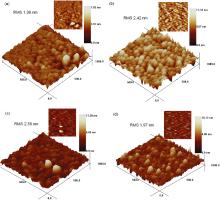
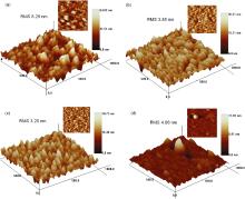
... It is well known that hydrazine hydrate, as a complementary complexing agent, improves the homogeneity and specularity of ZnS thin films in a reaction bath containing ZnSO4/NH3/(NH2)2/SC(NH2)2[25] ...
... a and Herrero[25] and Vidal et al ...
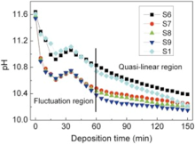
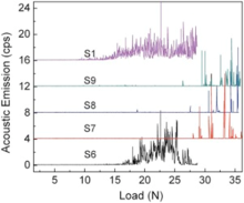
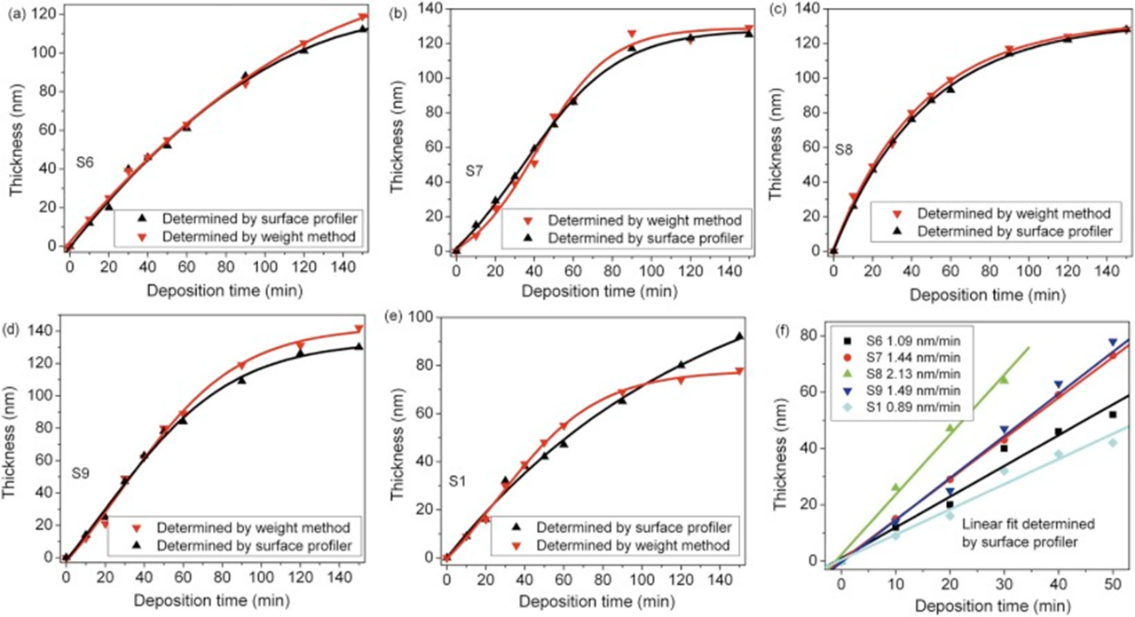
... Meanwhile, two regions of film growth from S6, S7, S8, S9 and S1 are displayed: an initial linear region and a final saturation one, which agree well with the literature[25,26,27,35] ...


 , Yanli Hong