Microstructure and Optical Properties of Yttrium-doped Zinc Oxide (YZO) Nanobolts Synthesized by Hydrothermal Method
[Sanjeev K. Sharma, Deuk Young Kim ]
]
]
|
|


In this work, yttrium-doped zinc oxide (YZO) nanopowder was synthesized via hydrothermal precipitation-method. The microstructure and optical properties of yttrium-doped zinc oxide nanopowder were characterized, which confirmed the well-crystalline wurtzite hexagonal phase of ZnO. The yttrium-doped zinc oxide nanopowder grains formed the nanobolts of ~400 nm in length and ~900 nm in width. High resolution-transmission electron microscopy (HR-TEM) of the nanobolts revealed uniform lattice fringes and no visible faults and/or distortions. X-ray photoelectron spectroscopy (XPS) analysis confirmed the presence of yttrium in the zinc oxide lattice, proving the contribution of yttrium on the microstructural and optical properties of the material. A strong ultra violet (UV) emission peak of the YZO exhibited a red shift compared to pure zinc oxide, which was ascribed to the defects and the formation of a shallow energy level caused by the incorporation of yttrium.
Zinc oxide (ZnO) has emerged as one of the most studied semiconductor materials because of its wide variety of applications (optoelectronics, chemo-/gas-sensors and antibacterial activity) due to wide direct band gap (3.37 eV) and high exciton binding energy (60 meV). It is an attractive material because of the excellent chemical and thermal stability[1, 2, 3, 4, 5, 6, 7]. Controllable synthesis of ZnO microstructure has been considered for the perspective of basic research and the realization of advanced devices[8, 9, 10]. The synthesis of nanosized ZnO particles is of great importance for both the fundamental study and the practical applications. Thus, the various synthesis methods, for example, hydrothermal[11], sol-gel[12], spray pyrolysis[13], and direct precipitation, [14] have been adopted for the growth of nanostructured ZnO having a uniform morphology. Among these techniques, a hydrothermal route is known as one of the excellent processes for synthesizing nanostructured ZnO ceramics because it is easy to handle, and allows us to tailor the morphology of the particles by controlling the rate, temperature, dopant concentration and duration of hydrolysis reactions[15, 16, 17].
To produce pure or doped ZnO nanocrystals, the metal impurities might be dependent on their concentration and the growth temperature, which significantly affects the defect concentrations in the crystals. In the same terms, dopants are purposely added to obtain or tailor defect-dependent properties of metal oxides. Nanostructured pure and doped-ZnO ceramics and thin films have been synthesized for the applications of optoelectronics, electromagnetics and sensors[18, 19, 20, 21, 22, 23, 24]. However, recently a rare-earth element, yttrium (Y), as a dopant in ZnO, named, Y-doped ZnO (YZO), has found a widespread use in various applications, including gas sensors[25], transistor[26], solar cells[27], and LEDs[28, 29]. It has been reported that Y improves the optical and electrical properties of YZO thin films and devices[30, 31, 32, 33]. For instance, Yang et al.[32] demonstrated tunable deep-level emission in YZO nanoparticles. Chen et al.[28]investigated the thermal stability of YZO films on GaN substrates. Kaur et al.[33]investigated the improvement in the electrical conductivity by incorporation of appropriate Y in the host ZnO structure. Lately, Heo et al.[34, 35] synthesized high quality of nanostructured YZO thin films at a low growth temperature. They investigated the appropriate concentration of Y for which the structural and electrical properties of YZO were improved. Despite ample work with respect to YZO films and devices as described above, a search of the literature did not produce any results with respect to the synthesis of YZO powder forming typical hexagonal grains (nanobolts). The morphology of pure and doped-ZnO is one of the key factors that determine the chemical and physical properties of the material.
In this study, we prepared pure and Y-doped ZnO (YZO) nanobolts by the hydrothermal synthesis technique. The effects of dopant (Y) concentration on the microstructural and optical properties of the YZO nanobolts were thoroughly examined.
Yttrium-doped ZnO (YZO) nanobolts were synthesized via simple hydrothermal-precipitation method. The solid reactants, zinc-nitrate-hexahydrate [Zn(NO3)2⋅ 6H2O] and hexamethylenetetramine (HMT) [C6H12N4], were dissolved in deionized water with equal concentrations (0.5 mol/L) to prepare the growth solution. Yttrium acetate hydrate [Y(CHCOO)3⋅ H2O] was used for Y dopant concentrations (2 at.% and 4 at.%). 0.5 mol/L sol was prepared and transferred into a 50 mL of ultrasonically cleaned teflon-lined autoclave. The autoclave was placed on the hot plate at 130 ° C for 3 h. After growth period of 3 h, the autoclave was taken out from the hot plate and cooled to room temperature. The obtained precipitates were filtered and washed thoroughly with DI water. The precipitate was dried in two steps in an oven (60 ° C: 1 h + 80 ° C: 2 h). These precipitates were transferred to quartz petri dish and annealed at 300 ° C for 3 h in an electric oven. The prepared powder was characterized by field emission-scanning electron microscopy (FE-SEM, Hitach S-4800), X-ray diffraction (XRD) analysis, X-ray photoelectron spectroscopy (XPS), high resolution-transmission electron microscopy (HR-TEM) and photoluminescence (PL).
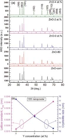
XRD was used to investigate the crystalline phase and purity of the synthesized YZO nanopowder. The XRD pattern of YZO nanopowder with respect to Y dopant concentration (Y: 0, 2, 4 at.%) is shown in Fig. 1(a). The sharp intense peaks of YZO nanopowder confirmed the polycrystalline nature of ZnO. The diffraction peaks originated from (100), (002), (101), (102), (110), (103), (200), (112), (201), (004) and (202) reflections were observed to be the hexagonal structure of ZnO[36, 37]. For the comparison of synthesized powder, the standard diffraction data of commercial ZnO powder (ZnO-com) was also inserted in the figure. The presence of prominent peaks of YZO showed that the films were polycrystalline in nature[21], and the relative intensities of the peaks were observed to be in a good agreement with those indicated by the Joint Committee on Powder Diffraction Standards (JCPDS) for the wurtzite structure of ZnO (JCPDS card No. 36-1451). The YZO crystals were grown along the same lattice direction of ZnO, independently of the Y dopants. However, the intensity of (002) peak increased by incorporation of Y concentration into ZnO lattice, which indicated that the refined and smooth YZO grains were observed with improved physical properties as shown in Fig. 1(a, b). The XRD peaks of both products (ZnO and YZO) were in good agreement with the JCPDS data (Card No. 076-0704). No peaks corresponding to other Y-containing or Zn-containing phases were detected in the XRD patterns, which might imply that Y had entered the lattices of ZnO[35].
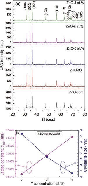 | Fig. 1. (a) X-ray diffraction patterns of ZnO-80 (dried at 80 ° C for 3 h) and YZO: 0 at.%, YZO: 2 at.%, YZO: 4 at.% (dried at 300 ° C for 3 h), and commercial ZnO powders (ZnO-com.); (b) lattice constant, c002 (nm) and crystallite size (nm) versus Y-dopant concentrations. |
Considering the diffraction (002) peak of bulk ZnO (as a reference point at 34.42° ), we could precisely locate the (002) peak of YZO nanopowder with respect to Y concentrations at 34.35° (Y: 0 at.%), 34.27° (Y: 2 at.%), and 34.19° (Y: 4 at.%). These peak angles were observed at lower diffraction angles than that of bulk ZnO. A blue shift of Δ θ = ~0.15° was observed in YZO nanopowder corresponding to an increase in the lattice constant to 0.0012 nm along the c-axis, owing to the larger ionic radius of Y3+ (0.092 nm) than that of Zn2+ (0.060 nm)[35]. Therefore, the Bragg's angle of YZO nanopowder decreased as the Y-dopant concentration increased. The lattice constant ‘ c’ for YZO (cYZO = 0.5229) was observed to be greater than that of pure ZnO (cZnO = 0.5207 nm) because of larger Y3+ions substituted into the host Zn2+ lattice sites. In addition, cYZO increased as the content of Y increased (Fig. 1(b)). The crystallite size was calculated by using Debye Scherrer's formula[38]: D(nm)=kλ (nm)/(β cosθ B), where k is a constant (k = 0.89), λ is the X-ray wavelength (0.154056 nm), β is the full width at half maximum (FWHM), and θ B is half of the diffraction angle. The crystallite size of YZO decreased from ~77 nm to ~70 nm as the Y dopant concentration increased from 0 to 4 at.% (Fig. 1(b)).
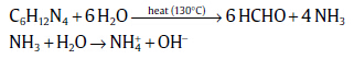
The mechanism of YZO nanopowder formation is described in terms of chemical reactions at a specified temperature. The Zn2+ ions are originated from Zn(NO3)2⋅ 6H2O and the OH- ions are derived from HMT as[39],
 (1)
(1)
and decomposition of ZnO occurs as
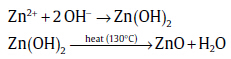 (2)
(2)As the concentration of Zn2+ and OH- ions exceeds the critical value, the precipitation of ZnO nuclei starts. Some ZnO nuclei initially form tiny single crystals aggregated together under the driving forces of surface energy, electrostatic force and so on. In the subsequent process, each nucleus in the aggregate grows isotropically along its c-axis. The complex [Zn(OH)4]2- was connected with the surface at both sites of a single ZnO nucleus. During a short time, each face of the first nucleus might have proceeded as the growth of nanobolts structure. This is the simplest and easiest process to form a nanobolts structure at a lower growth temperature of 130 ° C in aqueous solution. The aqueous solution was prepared by dissolving zinc nitrate hexahydrate, HMT, and yttrium acetate hydrate in 35 mL of DI water. When the aqueous mole concentration of zinc nitrate hexahydrate is relatively low, H2O would be abundant. This leads to the high concentration of hydroxide and impacts on the nucleation of ZnO nanocrystals. In other synthesis routes of hexagonal nanodisks, Alenezi et al.[40] reported the single crystal of ZnO hexagonal nanodisks synthesized by mixing the zinc sulfate and HMT at 75 ° C, while Pawar et al.[41]reported two synthesis steps with controlling of pH factor.
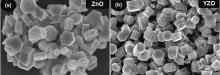
Fig. 2(a, b) shows the typical FE-SEM micrographs of the YZO nanobolts (Y: 0 at.% and Y: 2 at.%), respectively. The YZO nanoparticles were observed to be hexagonal nanobolts. As described in Eq. (2), the formation of Zn(OH)2 crystals was also observed in the XRD pattern made by the reaction from Zn2+ and OH- ions for the samples dried at 80 ° C in ambient (Fig. 1(a)). While the powders were annealed at 300 ° C in ambient conditions for 3 h in an electric oven, no Zn(OH)2 crystals were detected, which was confirmed by XRD pattern. For YZO nanobolts, the surface of the nanobolt grains seems to be more uniform and smoother than that of pure ZnO hexagonal grains. For ZnO grains, some pits were observed on the surfaces of the nanobolts that formed during the formation of the nanograins. YZO nanobolts were made hexagonally faceted like ZnO, but having flat surfaces on both ends. The diameter and the height of the nanobolts were observed to be around 900 nm and 400 nm, respectively. A similar kind of ZnO structure, named microdrum, was first reported by Krishna et al.[42], and this structure was obtained by aging a mixture of zinc nitrate with sodium salt for 12 h at 70 ° C, which is a time consuming process.
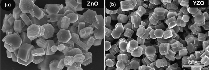 | Fig. 2. FE-SEM images of annealed nanopowder named nanobolts: (a) ZnO; (b) YZO. |
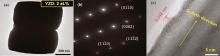
Further morphological and structural analyses of nanostructured YZO powders were carried out by using an HR-TEM. Fig. 3(a-c) shows the bright-field TEM image for a cleaved single YZO nanobolt, selected area electron diffraction (SAED) patterns and the magnified HR-TEM of typical YZO: 2 at.% nanobolts, respectively. Uniform contrast along the nanobolts reifies that the YZO nanobolt contained no visible structural defects and dislocations. The SAED pattern can be indexed to the reflection of the wurtzite ZnO structure, which is consistent with the above XRD results. From the magnified HR-TEM image, the interplanar lattice spacing was measured to be around 0.248 nm, which corresponds to the (101) plane of hexagonal ZnO, indicating that one of the growth planes of the ZnO nanobolts was along the (101) plane. The YZO nanobolt exhibited uniform lattice fringes and reveals no visible faults and/or distortions. This confirmed that the hydrothermally-grown YZO nanobolt was a high quality single crystal with no structural defects at an atomic scale. All of the above corroborate the YZO nanobolt to be purely crystallized with the wurtzite lattice structure through our hydrothermal synthesis techniques.
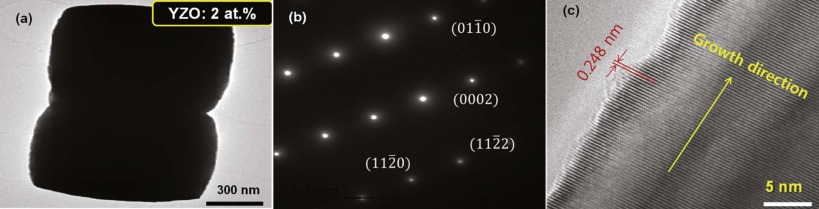 | Fig. 3. TEM analysis of typical YZO: 2 at.%, (a) bright-field TEM image for a cleaved single YZO nanobolts, (b) the selected area electron diffraction (SAED) patterns, and (c) HR-TEM image revealing the perfect lattice planes with no visible structural defects. |
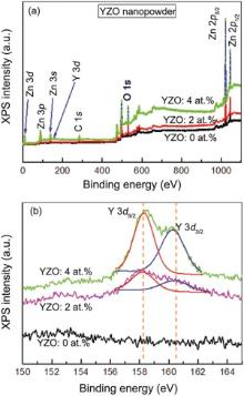
The chemical composition of nanostructured YZO powder was investigated via XPS. The XPS spectra of nanostructured YZO powders with respect to Y concentrations (0, 2 and, 4 at.%) are shown in Fig. 4(a). Different core levels were depicted, such as Zn 2p, O 1s, Zn 3p, Zn 3d, Y 3d, C 1s, the valence band region, and Auger transitions. No additional signals from other contaminations were observable except for a few Auger recombination peaks. The Zn 2p1/2 and Zn 2p3/2 peaks of the YZO powder were located at 1044.15 eV and 1021.05 eV, respectively. From Fig. 4(b), it is noted that the Y 3d peak was centered at 158.5 eV. These results depicted a high-purity of the YZO nanopowder. In high resolution, Y 3d core levels appear at increased binding energy positions, such as Y3 d5/2at 158.2 eV and Y 3d3/2 at 160.2 eV (Fig. 4(b)), which has almost a similar value as that of YZO thin films[35]. According to Ingo et al.[43], for Y 3d core levels of Y2O3, the Y 3d3/2, and Y 3d5/2 were observed at 157.4 and 156.6 eV, respectively. The discrepancies in these measurements arise from the different Y-O bond lengths between Y2O3 and the YZO crystal lattices. Hence, these results corroborate that our synthesized YZO nanopowder contained no Y2O3 precipitates.
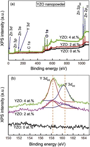 | Fig. 4. XPS survey scan spectra of YZO nanopowder (0, 2 and 4 at.%), (a) full survey spectra and represented the core level elements, and (b) high resolution of XPS spectra of Y 3d core level. |
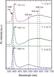
Microstructural properties of the semiconductor materials are closely related to the optical properties of ZnO/YZO because the structural defects and/or faults create the radiative recombination centers within the energy gap of the direct transition material. To study the optical properties of YZO, we measured the PL properties of the samples with respect to dopant concentrations. Fig. 5 shows the PL spectra of the YZO nanopowders (Y: 0, 2, and 4 at.%) with respect to the wavelength (nanometer scale) from UV to the visible range. The PL peaks were observed in two different regions, one is located in the UV region resulting from exciton emission and the other is located in the visible region resulting from deep level defect emission (DLE) associated with oxygen vacancies in the ZnO lattices. The pure ZnO exhibits a strong UV emission peak that centers at around 388 nm (3.2 eV), corresponding to the near band edge emission (NBE) that is attributed to the recombination of free excitons[44]. For the YZO nanopowders, the PL spectra are comprised of two peaks in NBE. The dominant peaks are centered at 394 nm for YZO: 2 at.% and at 396 nm for YZO: 4 at.%. In addition, the weak defect emission peaks were also observed at ~380 nm (3.27 eV) for both Y dopant concentrations, clearly indicating the effects of Y under NBE emission. The maximum intensity of the corresponding peak of ZnO was greater than that of YZO. The coordination tetrahedra of the Zn2+ and O2- ions are not perfect, but they are slightly distorted. When, the Y concentration increased in ZnO, the distortion was supposed to increase due to the presence of Y3+[26, 45]. The emission band of ZnO in the visible range was observed at a wavelength of 532 nm (2.33 eV), with a broad green emission band resulting from the recombination of photo-generated holes with singly ionized charge states in intrinsic defects, such as oxygen (O2-) and Zn interstitials (Zni)[46]. For YZO, the emission peaks in the visible range was shifted toward higher wavelength range, with a broad red emission band at a centered peak of 618 nm (2.01 eV) for Y = 2 at.% and at 635 nm (1.95 eV) for Y = 4 at.% due to increased defects by incorporation of Y concentrations. Additionally, the intensity of the red emission was enhanced remarkably centered at around 635 for 4 at.% YZO, which might be the result of increased Y concentration[47]. Compared to the PL peak of pure ZnO, the PL peak of YZO in the visible range was observed at a higher and longer wavelength region, allowing for deeper ion migration or light penetration[48].
 | Fig. 5. PL spectra of YZO nanopowder (Y: 0, 2, and 4 at.%) measured at room temperature. |
We synthesized highly crystalline YZO nanobolts from a mixture of zinc-nitrate-hexahydrate and HMT in DI water via hydrothermal precipitation at 130 ° C, with controlled Y-dopant concentrations. The SEM micrographs and XRD pattern analysis confirmed the presence of YZO hexagonal nanobolts. The SAED pattern indexed to the reflection of the wurtzite ZnO, which is in agreement with the XRD results. XPS spectra revealed that YZO nanopowder had a high purity with Y 3d core levels appearing at the binding energy of ~158.2 eV. Room-temperature PL spectra of YZO nanobolts showed a strong near band edge emission. The high crystal quality of the synthesized YZO nanobolts can be interpreted from the lower ionization energy of Y.
This research was supported by the Basic Science Research Program (NRF-2013R1A1A2059900), funded by the Korean government of Ministry of Education (MoE).
The authors have declared that no competing interests exist.
| [1] |
|
| [2] |
|
| [3] |
|
| [4] |
|
| [5] |
|
| [6] |
|
| [7] |
|
| [8] |
|
| [9] |
|
| [10] |
|
| [11] |
|
| [12] |
|
| [13] |
|
| [14] |
|
| [15] |
|
| [16] |
|
| [17] |
|
| [18] |
|
| [19] |
|
| [20] |
|
| [21] |
|
| [22] |
|
| [23] |
|
| [24] |
|
| [25] |
|
| [26] |
|
| [27] |
|
| [28] |
|
| [29] |
|
| [30] |
|
| [31] |
|
| [32] |
|
| [33] |
|
| [34] |
|
| [35] |
|
| [36] |
|
| [37] |
|
| [38] |
|
| [39] |
|
| [40] |
|
| [41] |
|
| [42] |
|
| [43] |
|
| [44] |
|
| [45] |
|
| [46] |
|
| [47] |
|
| [48] |
|