
Physical Mechanism and Performance Factors of Metal Oxide Based Resistive Switching Memory: A Review
[Cong Ye1 , Jiaji Wu1 , Gang He2  , Jieqiong Zhang
3 , Tengfei Deng1 , Pin He1 , Hao Wang1 ]
, Jieqiong Zhang|
|


This review summarizes the mechanism and performance of metal oxide based resistive switching memory. The origin of resistive switching (RS) behavior can be roughly classified into the conducting filament type and the interface type. Here, we adopt the filament type to study the metal oxide based resistive switching memory, which considers the migration of metallic cations and oxygen vacancies, as well as discuss two main mechanisms including the electrochemical metallization effect (ECM) and valence change memory effect (VCM). At the light of the influence of the electrode materials and switching layers on the RS characteristics, an overview has also been given on the performance parameters including the uniformity, endurance, the retention, and the multi-layer storage. Especially, we mentioned ITO (indium tin oxide) electrode and discussed the novel RS characteristics related with ITO. Finally, the challenges resistive random access memory (RRAM) device is facing, as well as the future development trend, are expressed.
The resistive switching (RS) phenomenon was firstly reported in a series of binary oxides by Hickmott in 1962[1]. Until now, the scientific and industrial interests on the resistance random access memory (RRAM) have already lasted for more than 50 years. Extensive research on the physical analyses and mechanisms has been performed to understand the electrical phenomena in the 1960s and 1970s[2, 3, 4, 5, 6]. In fact, there are various candidates (e.g. magnetic random access memory [MRAM], ferroelectric random access memory [FRAM], phase change random access memory (PRAM) and resistive random access memory [RRAM][10, 11, 12, 13, 14, 15, 16]) for next-generation memory to replace current flash memory for its disadvantages of high operating voltage, low operating speed, high power consumption and the scaling limitation to 16 nm[7, 8, 9]. Fortunately, RRAM has been considered to be the most promising one, owing to its advantages of simple structure, low operating power and fast switching speed[17, 18]. The RRAM structure is a switching layer sandwiched between two metal electrodes, which is a metal-insulator-metal (MIM) structure. It has been found that a great variety of materials including transition metal oxides, perovskite, organic materials have shown RS characteristics[19, 20, 21, 22]. Owing to the extreme diversity of RS materials, it is not possible to review all the related issues. Among them, metal oxide based resistive switching memory is widely investigated due to its simple composition, low cost, and compatibility with CMOS (complementary metal-oxide-semiconductor transistor) technology, such as NiO[23, 24, 25, 26], TiO2[27, 28, 29, 30, 31], ZrO2[32, 33], Al2O3[34, 35], HfO2[36, 37, 38, 39, 40, 41], ZnO[42, 43, 44], and WO3[45]. It has been reported that memory cells such as TiN/TiOx/HfOx/TiN have shown switching speed of ~5 ns [46]. Lee et al.[47] demonstrated a TaOx-based asymmetric passive switching device with extreme cycling endurance of over 1012. Furthermore, the structure of TiN/HfOx/Pt exhibited data retention properties of 104 s at 85 ° C[48]. In summary, research has indicated that excellent performance of ultrahigh switching speed, good switching endurance and reliable data retention has been achieved in metal oxide based resistive switching memory.
In this review, we focused on the metal oxide based RRAM. Although we limit to the metal oxide in this review, there are still some meaningful work needed to be summarized. Recent research on RRAMs still faces challenges such as wide resistance distribution and non-uniformity of SET/RESET voltage. Also, the physical mechanism in the SET/RESET process for RRAM is still unclear. Therefore, at first, the basic working principles of the device and the switching mechanism will be highlighted in Sections 2 and 3. Secondly, the effect of electrode materials and the structure of switching layers on the performance parameters including uniformity and power consumption will be critically discussed in Sections 4 and 5. Finally, an outlook for RRAM application and its challenges current being faced such as high power consumption, operating stability and controversial RS switching mechanisms will be presented.
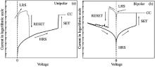
The RS characteristics of metal oxide RRAM can be classified into two switching modes: unipolar and bipolar. Unipolar RS behavior refers to the switching direction depending on the amplitude of the applied voltage rather than the polarity, as illustrated in Fig. 1(a). Bipolar RS behavior refers to the switching direction dependent on the polarity of the applied voltage, and thus the set process can only occur at one polarity and the reset process can only occur at reverse polarity, as shown in Fig. 1(b). The compliance current is an important parameter to be considered in the set process for both unipolar and bipolar RRAM. It is recommended to enforce a set compliance current to avoid a permanent breakdown of the device[49]. In addition, changing the value of compliance current and stop voltage can realize multilevel storage for the RRAM. Section 5 will describe it in detail[46].
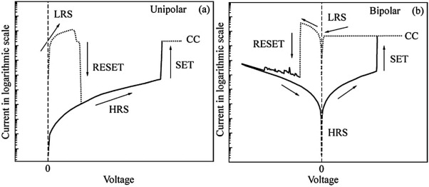 | Fig. 1. Typical I-V curves of unipolar (a) and bipolar (b) switching modes and the current compliance (CC) is adopted to avoid permanent dielectric breakdown of devices [49]. |
As for a unipolar RRAM, the device usually has a symmetric structure, which means that the same material has been used as the top electrode (TE) and the bottom electrode (BE), such as Pt/NiO/Pt[50], Pt/TiO2/Pt[51], Pt/ZnO/Pt[52], Pt/ZrO2/Pt[53], Pt/HfO2/Pt[54]. In contrast, the device structure of bipolar switching is usually asymmetric, which means that different materials are used as TE and BE, such as Pt/NiO/SrRuO3[55], Pt/TiO2/TiN[56], TiN/ZnO/Pt[52], Ti/ZrO2/Pt[57], and TiN/HfO2/Pt[48]. For different switching modes, the reset mechanism is a controversial issue. Based on the conducting filament (CF) theory, it can be classified into two main CF disruption mechanisms: thermal dissolution model[26]and ionic migration model[58]. The former is often explored to explain the unipolar RS characteristics, whereas the latter can be normally applied to explain the bipolar RS characteristics. It is reported that the reset mechanism is greatly dependent on the electrode/oxide interfaces[38]. For unipolar RRAM, noble metals such as Pt or Ru are often applied as both top and bottom electrodes. On the other hand, the bipolar RRAM active materials such as TiN or Ti are normally used as electrodes, and the interfacial layer is easy to be formed in the operating process. Yu and Wong[59] proposed a universal reset mechanism for both unipolar/bipolar modes. Firstly, for the unipolar device, the mainstream viewpoint of reset mechanism is due to a thermal dissolution of CFs by local Joule heating[60, 61, 62]. Oxygen ions (O2-) would be accumulated near the anode with a concentration gradient during the set process. Subsequently, the Joule heating would activate O2- to combine with the oxygen vacancies (V02+) during the reset process to make the CF disconnect. This thermal dissolution model results in the unipolar reset process. However, Yu et al.[63] put forward a question about this: if the CF is considered to be “ dissolved” by local Joule heating, the CF may rupture in the middle of the filament where the temperature is the highest[64] rather than occur at the region near the anode.
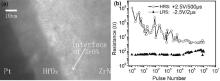
As concerned as the bipolar device, the interfacial layer may act as an oxygen diffusion barrier, and thus the thermal diffusion mentioned above is not sufficient to result in the reset process. Only by the application of a reversed electric field can the oxygen ions drift back to cause the CFs to rupture. This is a so called ionic migration model. As the interfacial oxide layer was observed, Yu et al.[63] maintained that it may act as an “ oxygen reservoir” , which stores the oxygen ions during the set process and then drives them back during the reset process. Besides, the “ oxygen reservoir” can prevent the oxygen from escaping from the device to ambient. Therefore, this concept of an “ oxygen reservoir” is envisioned, which can explain some switching characteristics for bipolar RRAMs. For example, in Fig. 2(a), the formed interface of ZrON can serve as an oxygen reservoir to hamper the oxygen ions' diffusion further away from the RS layer HfOx and provide sufficient oxygen ions in the reset process, which is attributable to the robust cyclic endurance property of Pt/HfOx/ZrNx memory cell, as demonstrated in Fig. 2(b)[65].
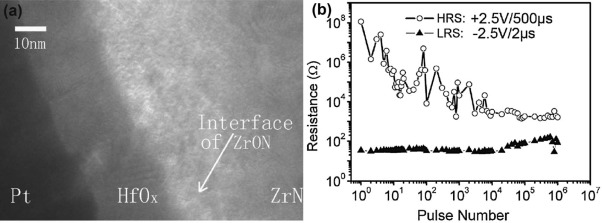 | Fig. 2. (a) The cross-section TEM image of Pt/HfOx/ZrNx stacks. (b) Endurance characteristics of the Pt/HfOx/ZrNx structure in the electric pulse switching mode [65]. |
The origin of RS behavior can be roughly classified into the conducting filament type and the interface type[66]. Here, we adopt the filament type to study the metal oxide based resistive switching memory, which considers the migration of metallic cations and oxygen vacancies. Accordingly, we discuss two main mechanisms: the electrochemical metallization effect (ECM) and the valence change memory effect (VCM).
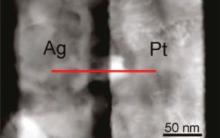
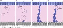
In general, ECM can be adopted to explain RRAM which consists of an electrode made from an electrochemically active metal, such as Ag[19], Cu[67], or Ni[68], and an electrochemically inert metal counter electrode such as Pt[69], Au[70], or Ir[71]. Yang et al.[19] studied Ag/ZnO:Mn/Pt memory cell and successfully observed nanoscale Ag conductive bridge penetrating through the storage thin film by scanning transmission electron microscopy (STEM) with high-resolution energy dispersive X-ray spectroscopy (EDX), which could account for the high conductivity in the ON-state device, as shown inFig. 3. Fig. 4 illustrates a schematic diagram for the switching mechanism of Ag/ZnO:Mn/Pt devices. When a positive voltage is applied to Ag TE, oxidation process of Ag atoms occurs and Ag+ cations are generated, which could be described in Fig. 4(a). The Ag+cations drift to Pt BE under the electrical field and are reduced by electrons flowing from the cathode as shown in Fig. 4(b). The successive precipitations of metal atoms at the cathode lead to a growth of the Ag protrusion, which finally reaches the TE and forms a conductive path in the ON state as shown in Fig. 4(c). When the polarity of the applied voltage is opposite, an electrochemical dissolution takes place somewhere along the bridge, and switches to the OFF state (Fig. 4(d)). In Fig. 3, the conductive bridge composed of Ag can be detected at ~8 nm underneath the bridge/Pt interface. This result shows that the conductive bridge has not only connected the electrode pair completely but also extended into Pt BE. Based on the above examples, we believe that more studies about manipulation or observation on the CF need to be carried out to further prove ECM mechanism. Based on the above examples, we believe that the ECM mechanism does not always prevail whenever electrochemically active metals such as Cu or Ag are utilized in a resistive switching cell. In the reported Cu/Cu-TCNQ/Al (TCNQ denotes 7, 7′ , 8, 8′ -tetracyanoquinodimethane) memory cell thirty years ago, a charge transfer reaction between Cu and TCNQ was claimed to be responsible for the resistive switching effect; subsequently, a variety of control experiments indicated that the resistive switching was due to the Al oxide/Al hydroxide layers acting as the electrode[72, 73]. In consequence, as for ECM effect, when Cu or Ag is selected as the electrode for RRAM, the certain mechanism needs to be verified by specific experiment.
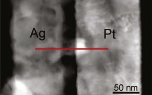 | Fig. 3. Z-contrast image and high-resolution EDX analysis in STEM mode for the bridge-like region in ON-state device. A line profile concerning the intensity of Ag along the bridge [19]. |
 | Fig. 4. A schematic diagram for mechanism of resistive switching effect in ECM cell: (a) Ag oxidize to ions at the Ag electrode(Ag → Ag+ + e-); (b) Ag+ migrate to Pt electrode and is reduced therein(Ag+ + e-→ Ag); (c) precipitations of Ag at the Pt electrode and finally form a highly conductive filament in the cell, setting the system into LRS; (d) an electrochemical dissolution of the filament takes place, resetting the system into HRS[19]. |
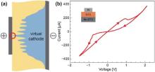
As concerned as the valence change memory effect (VCM) RRAM, it has much difference with RRAM. It is not necessary to consist of an active electrode and an inert electrode. Here, we take the structure of Pt/STO/Nb-STO as an example to illustrate the VCM memory. The ions' migration micro-process is as follows: When the positive bias is applied on the Pt electrode, a large amount of Vo2+ would accumulate on the Nb-STO electrode, and these Vo2+ would form the similar trapezoid shape of “ actual cathode” as shown inFig. 5(a)[74]. The area of “ virtual cathode” would increase by the improvement of positive bias, and Vo2+ would reach the anode finally. At the same time, oxygen ions near the anode lose electron and produce O2 bubble. The VCM cells switch from high resistance state (HRS) to low resistance state (LRS).
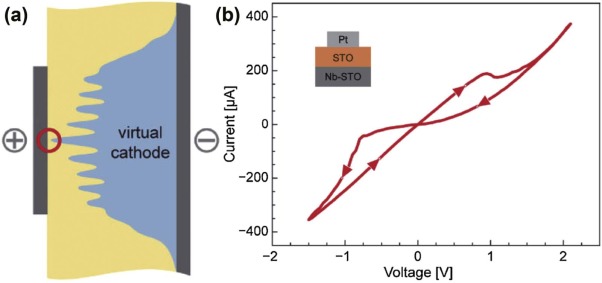 | Fig. 5. (a) Trapezoid shape of “ virtual cathode” was formed under the positive bias. (b) Typical I-V curves of Pt/STO/Nb-STO device [74]. |
When negative bias is applied, the O2- migrates to cathode and combines with the oxygen vacancies. This conductive path will be disconnected, the cell switched from LRS to HRS. The typical I-V curves of Pt/STO/Nb-STO memory device are as shown in Fig. 5(b). Especially, more studies about manipulation or observation on the CF need to be carried out to further prove VCM mechanism.
Electrode materials play an important role in the RS property[52, 75, 76]. In general, when the electrode is selected for the RRAM device, the following key factors of the electrode material should be mainly considered: the activity of the electrode, work function, and the interface between the electrode and the switching layer for the RRAM device[77]. Seo et al.[78] found that the RS behavior for NiO films based RRAM is dependent on the interface barrier height between the electrode and the switching layer. When Pt or Au is used as the top electrode, Ohmic contact is formed and the voltage drop between electrode and switching layer can be ignored, and thus a relatively low voltage can induce the resistive switching[79]. When Ti is used as the top electrode and Schottky contact is formed, the voltage drop should be considered and a higher voltage is needed to induce the resistive switching. Meanwhile, Yang and Rhee[80] also reported the similar results by investigating the structure of Pt/Cu2O/bottom electrode. In Table 1, some commonly used electrode materials were summarized for metal oxide based resistive switching memory.
| Table 1 Summarized electrode materials on the metal oxide based resistive switching memory |
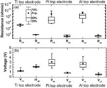
In most cases, the unipolar RS behavior is obtained with a noble metal electrode, such as Pt or Ru. If one of the electrodes is replaced by active electrode such as Ti or TiN, the bipolar RS behavior is obtained. It is reported that the RS uniformity of the RRAM device can be improved by utilizing Ti as the electrode[52]. In comparison with Pt/ZrO2/Pt and Al/ZrO2/Pt, Lin et al.[52] found that the structure of Ti/ZrO2/Pt device showed a narrower distribution of switching parameters, such as Ron and Roff, Von and Voff as shown in Fig. 6. Meanwhile, metal electrodes, such as TiN, TaN and ZrNx, also show excellent performance for RS memory. For example, the structure of ZrNx/HfOx/Pt exhibits better endurance (> 106) and longer retention time (104 s) by comparing with the Pt/HfOx/Pt [65]. This is possibly attributed to the formation of ZrON interface, which is served as an “ oxygen reservoir” , and thus improves the performance and reliability of the device [92-95].
 | Fig. 6. Variations of the resistance and voltage parameters on ZrOx RRAM (Ron and Roff measured at 0.3 V)[52]. |
Besides, we discuss another important active electrode: ITO electrode. This transparent electrode has already been utilized in many electronic devices, as well as memory units because of its excellent conduction, light transmittance, and high hardness[96, 97]. Moreover, it is a highly degenerate n-type semiconductor and its good conductivity originates from the carriers including oxygen vacancies and the activated Sn4+ ions on In3+ sites. We have reported the TiN/HfOx/ITO memory cells, which shows self-compliance current phenomenon as shown in Fig. 7(a). The reason why ITO electrode has a small Vsetis clarified by discussing a possible resistive mechanism as illustrated in Fig. 7(b).
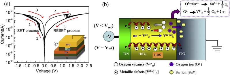 | Fig. 7. Switching characteristic curves of TiN/HfO2/ITO device for 10 switching cycles with increasing voltage are shown, LRS current increases slightly and shows self-compliance to 800 µ A (ICOMP). (b) In SET process, schematic diagram of driving mechanism for TiN/HfO2/ITO memory cell is given. The redox reactions to form the conducting filament are shown together[48]. |
According to the CF theory, the filament is made of oxygen vacancies or metallic ions. If the ITO electrode is applied in RRAM, the existence of many Sn4+ ions may affect the drift of O2- in the HfO2 layer because Sn4+ ions are active and flexible to move in the ITO film. This would result in the difference in CF formation/rupture, which in turn induces the different switching behavior. We have done much work on ITO electrode and found that ITO electrode can relate to the redox process in the MIM cell, which have advantages on the improvement of RS performance, such as reducing the power consumption of the device, providing robust endurance and so on[42].
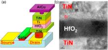
An electrode with a buffer layer is usually adopted to improve the RS characteristics of the RRAM device. Fig. 8(a) illustrates a schematic diagram of 1T1R unit (1 Transistor and 1 RRAM). The transistor is cascaded with a stacked TiN/Ti/HfO2/TiN RRAM cell to provide compliance current. Fig. 8(b) shows the HR-TEM image of TiN/Ti/HfOx/TiN stacked layers[98]. Lee et al.[46] reported that this kind of 1T1R structure exhibited excellent RS performance, including high-speed operation (< 10 ns), large ON/OFF ratio (> 100), long high-temperature lifetime, multilevel storage, high device yield (~100%), and the TiN/Ti/HfO2/TiN memory cells have been successfully integrated in a 0.18 µ m COMS process. Considering the TiN/Ti electrode, the buffer layer Ti film served as a capping layer, which can deplete the oxygen atoms from the HfOx thin film and act as an oxygen reservoir. Also, this group also used AlCu and Ta as the capping layer for the HfOxmemory cell, and the device exhibited stable bipolar switching behavior but had a small ON/OFF ratio (~4) [89]. The oxygen capture ability of capping metal layer may be responsible for these results[98].
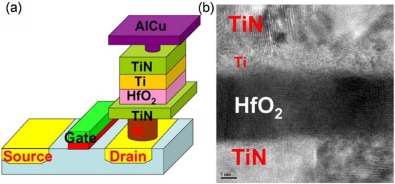 | Fig. 8. (a) A typical 1T1R structure of RRAM with HfOx; (b) HR-TEM image of the TiN/Ti/HfO2/TiN stack with 20 nm thick HfO2 layer[98]. |
In addition, Govoreanu et al.[99] reported the TiN/Hf/HfOx/TiN RRAM stack with the size of 10 nm × 10 nm, which has become the smallest HfO2-based RRAM cell in the research field so far. It can be seen that TiN electrode is also designed with Hf thin film as the buffer layer. We can conclude that different capping layers lead to the variation of RS behavior, and hence selecting the material as the buffer layer is crucial.
Despite the commonly used electrodes as mentioned above, researchers intend to find the applications of novel materials to the RRAM devices, such as carbon nanotube, n+-Si, and graphene. Chai et al.[85] have reported switching characteristics of an amorphous carbon (a-C) layer with carbon nano-tube (CNT) electrodes for ultra-dense memory. The device was proposed for solving the sneak leakage current in cross-point memory, which successfully further increased the density of the memory.
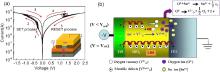
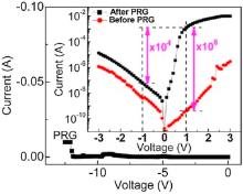
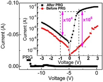
Moreover, n+-Si electrode, which is normally used in the transistor, also can be used in RRAM device. Fig. 9 shows the typical I-V curves of n+-Si/ZrO2/Pt memory cell before and after programming progress, which demonstrated that resistance ratio (ON/OFF) exceeds 106 with a 1 V readout voltage. Especially, a pronounced self-rectifying effect, with the rectification ratio as high as 104, is observed after programming process. The emergence of self-rectifying effect might be that the current conduction is suppressed by the Schottky barrier, which exists in the interface between n+-Si electrode and SiOx/ZrOx layers [86].
 | Fig. 9. The typical I-V curves of n+-Si/ZrO2/Pt structure, a pronounced self-rectifying effect is obtained after programming[86]. |
At the same moment, many devices, such as n+-Si/HfOx/Ni [100], Ni/AlOy/n+-Si[101], and n+-Si/ZrO2/Pt[86], have shown the self-rectifying effect as a result of using n+-Si electrode. As we already know, self-rectifying property can largely alleviate the crosstalk in crossbar array without extra rectifying diodes, which correspond to the 1D1R (one diode-one resistance). Therefore, the memory with self-rectifying properties has potential applications in high-density crossbar memory.
It was reported in 2008 that the CMOS process node would be scaled to 22 nm in 2014, which was near to the limit[102]. To meet the urgent need of an increase in storage density for RRAM development, it is very challengeable for RRAM to achieve further scaling down. Therefore, it is difficult to achieve an obvious increase of storage density only through the simple scaling down of the device size. However, multilevel storage can significantly enhance the storage density without much change in current technologies. Multilevel storage refers to the ability of a memory cell to exhibit reproducible resistive switching between multiple resistance states and store multiple values consequently[102]. Lee et al.[46] proposed that multilevel storage can be achieved by controlling either compliance current (Icomp) or operating voltage. In this chapter, we mainly considered the doping effect on the metal oxide switching layer, as well as the structure design of the switching layer.
To clarify the influence of doping on the switching layer, Lee et al.[103] investigated various doped metal oxides and found that doping in the switching layer for RRAM can realize favorable memory characteristics such as reliability under programming cycles, good data retention, potential multi-bit operation, highly scalable property, and fast switching speed.
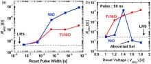
Low-power and high speed resistive switching of Pt/Ti:NiO/Pt memory cell has been reported[104]. Because of doping the Ti into the NiO memory, this memory achieved a faster reset time (< 5 ns) than that of the pure NiO film, as shown in Fig. 10(a). In addition, the abnormal set phenomena in the pure NiO film as illustrated in Fig. 10(b), can also be suppressed, for the reason that an oxygen reservoir was introduced and Ti-O bonds were formed due to the Ti doping.
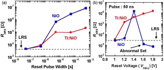 | Fig. 10. Comparison of the reset speed between NiO and Ti:NiO at: (a) Vcell = 1.0 V, (b) Vcell = 1.6 V, abnormal set phenomena occur during the reset process[104]. |
On the other hand, some doping effect can be presented as forming-free for the memory cell. For TiN/Ge:HfO2/Pt memory cell[105], the Ge atoms diffused into the HfO2 layer and the oxygen vacancies increased, and thereby the memory is forming-free. Moreover, the uniformity of this cell is greatly enhanced by Ge doping, due to the low oxygen-vacancy formation energy. In particular, the self-compliance current phenomenon is achieved. Wang et al.[106] reported that Pt/Cu:HfO2/Pt memory demonstrated good electrical characteristics: DC endurance over 100 cycles, a long retention over 105 s, a fast operation speed and large storage windows about 107 in 9 µ m2 devices. Among these performance parameters, the endurance refers to the number of set/reset cycles[107]. In general, typical flash shows a maximum number of write cycles between 103 and 107, and accordingly, RRAM should provide at least the same endurance, and even a better one[108]. Retention refers to the data retention time, the length of time of a memory cell should stay in one state after programming or erasing[109]. For RRAM device, the data generally need to be stored more than ten years. During this process, it needs to consider the influence of the temperature and continuous voltage signal of read operation. In short, doping in the switching layer is an effective way to improve the performance of RRAM.
To make a further study on the potential applications of high k based RRAMs, the structure of switching layer is needed to design for the excellent performance and reliability of RRAM device, including the low power consumption and good uniformity [110-112]. Double-layer structure RRAM is proven to be a feasible and effective way[97]. For example, Ni/GeOx/HfON/TaN RRAM has been reported with a very low set current of 0.1 µ A and reset current of -0.3 nA, GeOx was served as the switching layer while HfON was used as the charge-trapping layer, which contributed to the ultra-low switching power of the device [84].
As for the bi-layer structure, the role of each layer is different. One layer with lower resistivity can act as series resistance, and the other one has higher resistivity[113]. Normally, the RS behavior does not occur in the whole layer but occurs in the higher resistivity switching layer, and the lower resistivity layer can improve the resistance of ON state. The higher resistance value of ON state would bring out lower reset current (Ireset) and power consumption.
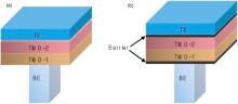
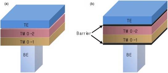
Many bi-layer devices can obtain the low power consumption. A typical example of Barrier/TMO1/TMO2/Barrier structure device is shown in Fig. 11, which exhibits the set power consumption ~3 µ W and power consumption ~80 nW. Compared with the previous TMO2/TMO1 structure without the barrier, the set current of Barrier/TMO1/TMO2/Barrier structure reduces from 50 µ A to 1 µ A, and the reset current reduces to 30 nA as shown in Fig. 12<sup>[114].
 | Fig. 12. Typical I-V characteristic of Barrier/TMO1/TMO2/barrier. (b) Typical I-V characteristic of TMO1/TMO2without barrier layer[114]. |
In Table 2, some low power RRAM devices are summarized. By the comparison of the Iresetand power consumption between the bi-layer and the single layer, we conclude that the reduction in power consumption might be due to the application of the bi-layer.
| Table 2 Low power RRAM devices are summarized |
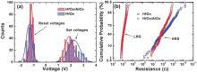
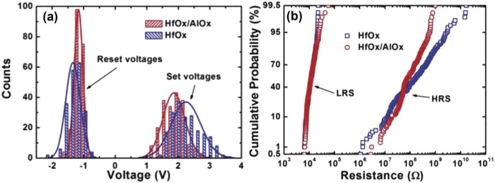
Apart from low-power consumption mentioned above, good uniformity can also be obtained by the application of bi-layer structure. Uniformity is the variation of the resistance switching including temporal fluctuations (cycle to cycle) and spatial fluctuations (device to device). It mainly consists of device parameters such as set voltage, reset voltage, and HRS and LRS resistance distribution, which are essential to large-scale manufacture of RRAM[38]. To understand the relationship between bi-layer structure and uniformity, the characteristics of TiN/HfOx/Pt and TiN/AlOx-HfO2/Pt[117] memory cells have been investigated. By embedding a thin AlOx buffer layer (~5 nm) between the HfOxand the TiN top electrodes, the TiN/AlOx-HfOx/Pt cell exhibited much better characteristics. In particular, HfOx/AlOx bi-layer RRAM devices show a better switching uniformity of the switching voltages and resistances distribution than the single layer HfOxdevices, as shown in Fig. 13. The improvements of the uniformity in the HfOx/AlOx bi-layer device might be because the diffusion of Al atoms into HfOx could stabilize the CFs to reduce the randomness of RS [118]. Another explanation is that the reset process usually can only rupture the upper part of the CFs, and the so-called “ virtual cathode” in the bottom AlOx layer tends to serve as the seeds to re-grow the CFs. However, further work is still needed to clarify the reason for the improvement of uniformity.
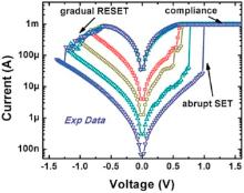
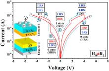
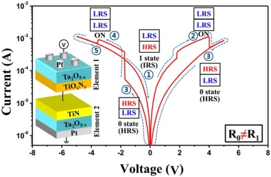
In addition to the bi-layer structure, the application of multi-layer structured memory cell also exhibits excellent performance. Fang et al.[119] present the four layer structure of TiN/HfOx-TiOx-HfOx-TiOx/Pt memory cell; compared with HfOx-based single-layer device, a multi-layer device achieves the forming-free behavior. Moreover, the uniformity of parameters, such as set and reset voltage, HRS and LRS resistance distributions are significantly improved. It is possible that Ti doping effect and the confinement of conduction filament within different dielectrics layers contribute to the improvement of uniformity. Based on this structure, Yu et al. [120] have engineered oxide-based synaptic devices by stacking multiple layers of Pt/HfOx/TiOx/HfOx/TiOx/TiN (from bottom to top). Stacked multi-layer can be applied to the potential and attractive application of neuromorphic computing, which could emulate the brain and realize visual image processing and understanding or auditory speech recognition [121]. Their group gradually modulated hundreds of resistance states by applying hundreds of identical pulses, and this referred resistance modulation methodology has an obvious advantage over the previous widely used methodology of varying pulse amplitude or width [122, 123], which will greatly simplify the neuron circuit design and optimize the oxide-based resistive switching electronic synaptic device. Furthermore, the multi-level resistance states based on this structure were achieved by varying the sweep stop voltages shown in Fig. 14. It can be seen that the set process is abrupt while the reset process is gradual. We may ask whether the gradual reset process is necessary for the achievement of the multi-level storage. Moreover, another issue should be considered, whether resistance modulation in this oxide-based synaptic device is resulted from the interface defects between each layer (HfOx/TiOx). To highlight the possibility of high-density application of RRAM, Lee et al.[124] investigated the Pt/Ta2O5-x/TiOxNy/TiN/Ta2O5-x/Pt matrix and found two bipolar resistive switching elements on the structure of Pt/Ta2O5-x/TiOxNy and TiN/Ta2O5-x/Pt as illustrated in Fig. 15. The four layer structure exhibited multi-level storage function and at each crossbar point with three distinguishable resistance states (HRS, LRS and IRS). In summary, the application of a multi-layer structure is potential for the structure design of RRAM and an effective way to improve its performance.
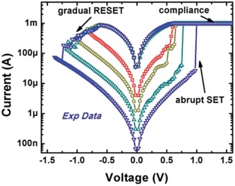 | Fig. 14. Typical DC I-V bipolar switching curves of oxide based synaptic devices. The multilevel states in this measurement are achieved by changing RESET stop voltages [120]. |
A basic overview of RRAM devices is given. Basic working principle and switching mechanism are summarized. There are other mechanisms in the same or different RS materials, which could not be totally covered in this review. Finally, we mainly discussed the effect of electrode materials and switching layer on the performance parameters.
In further pursuit of high speed and low power, researchers have become increasingly intrigued with RRAMs as a promising candidate for next generation non-volatile memory (NVM). Common parameters are used for monitoring the reliability of RRAM devices, such as retention time, cycling endurance, on-to-off ratio, and on-state current. From the perspective of technological application, several important issues should be also taken into consideration as follows. The first and foremost is scalability. With the switching cells down to the nanoscale, it is accompanied by inherent physical limits and technical barriers. The configuration and geometry of CFs in the host insulating matrix and thermal crosstalk between neighboring cells may play a critical role in RRAMs. Moreover, stability is thought to be not ignored. Generally, LRS and HRS of switching cells are not energetically stable, especially when switching cells are subjected in some specific conditions, like the severe stationary or the alternating stimulation, which will seriously affect the retention and endurance. Because the lifetime of CFs is a primary factor for the stability of RRAMs, it is essential to select proper switching and electrode materials.
The development of RRAM test chips until February 2014 is summarized in Table 3[102], which indicated the progress form primary reported programming/erasing properties to current product application. Although the development of RRAM has progressed rapidly in the last five years, there are still some unsolved issues and problems waiting for further study to be clearly elucidated. Questions involving the high power consumption, low endurance, and non-uniformity in the switching parameters are requiring further attention. Although the excellent performance in RRAMs was reported in some research, e.g. a retention time for over 10 years at a high-temperature measurement or a memory endurance of over 106 cycles, there is little information about characteristic variations from cell to cell and from chip to chip. Additionally, considering the different degree of operation stability for various resistive switching materials, the effect of defects in switching layers, and interface properties between the electrode and the switching layer, it is significant and necessary to make a deeper understanding of the switching mechanism from a microscopic point of view. A clear understanding of resistive switching mechanisms will contribute to explore the essence of resistive behavior, more importantly, which also has great significance on the improvement of performance parameters. More research efforts are also needed in the optimization of process and material as well as the improvement of fabrication technology. For further study, an important research direction is to find RS material systems with environment-friendly, compatibility with CMOS technology and excellent performance parameters. Based on the continuing work, we are convinced that resistive-switching RRAM devices will bring a breakthrough of technology and achieve success in future non-volatile memory application.
| Table 3 RRAM test chips have been reported on famous international IC conference until 2014[31] |
The authors gratefully acknowledge the financial support from the National Natural Science Foundation of China (Nos. 61474039 and 51572002), and the Nature Science Foundation (Key Project) of Hubei Province (No. 2015CFA052).
The authors have declared that no competing interests exist.
| [1] |
|
| [2] |
|
| [3] |
|
| [4] |
|
| [5] |
|
| [6] |
|
| [7] |
|
| [8] |
|
| [9] |
|
| [10] |
|
| [11] |
|
| [12] |
|
| [13] |
|
| [14] |
|
| [15] |
|
| [16] |
|
| [17] |
|
| [18] |
|
| [19] |
|
| [20] |
|
| [21] |
|
| [22] |
|
| [23] |
|
| [24] |
|
| [25] |
|
| [26] |
|
| [27] |
|
| [28] |
|
| [29] |
|
| [30] |
|
| [31] |
|
| [32] |
|
| [33] |
|
| [34] |
|
| [35] |
|
| [36] |
|
| [37] |
|
| [38] |
|
| [39] |
|
| [40] |
|
| [41] |
|
| [42] |
|
| [43] |
|
| [44] |
|
| [45] |
|
| [46] |
|
| [47] |
|
| [48] |
|
| [49] |
|
| [50] |
|
| [51] |
|
| [52] |
|
| [53] |
|
| [54] |
|
| [55] |
|
| [56] |
|
| [57] |
|
| [58] |
|
| [59] |
|
| [60] |
|
| [61] |
|
| [62] |
|
| [63] |
|
| [64] |
|
| [65] |
|
| [66] |
|
| [67] |
|
| [68] |
|
| [69] |
|
| [70] |
|
| [71] |
|
| [72] |
|
| [73] |
|
| [74] |
|
| [75] |
|
| [76] |
|
| [77] |
|
| [78] |
|
| [79] |
|
| [80] |
|
| [81] |
|
| [82] |
|
| [83] |
|
| [84] |
|
| [85] |
|
| [86] |
|
| [87] |
|
| [88] |
|
| [89] |
|
| [90] |
|
| [91] |
|
| [92] |
|
| [93] |
|
| [94] |
|
| [95] |
|
| [96] |
|
| [97] |
|
| [98] |
|
| [99] |
|
| [100] |
|
| [101] |
|
| [102] |
|
| [103] |
|
| [104] |
|
| [105] |
|
| [106] |
|
| [107] |
|
| [108] |
|
| [109] |
|
| [110] |
|
| [111] |
|
| [112] |
|
| [113] |
|
| [114] |
|
| [115] |
|
| [116] |
|
| [117] |
|
| [118] |
|
| [119] |
|
| [120] |
|
| [121] |
|
| [122] |
|
| [123] |
|
| [124] |
|
| [125] |
|
| [126] |
|
| [127] |
|
| [128] |
|
| [129] |
|
| [130] |
|
| [131] |
|
| [132] |
|
| [133] |
|
| [134] |
|
| [135] |
|
| [136] |
|
| [137] |
|
| [138] |
|
| [139] |
|