

Controllable Synthesis of Well-aligned ZnO Nanorod Arrays on Varying Substrates via Rapid Electrodeposition
[Haibao Zhang1, 2 , Shaowei Jin1, *  , Guotao Duan
2, ** , Jingjing Wang2 , Weiping Cai2 ]
, Guotao Duan, Jingjing Wang|
|


*Corresponding author. Prof., Ph.D.; Tel.: þ86 551 63861257; Fax: þ86 551 63861810; E-mail address:jinsw@mail.ustc.edu.cn (S. Jin)
** Corresponding author. Ph.D.; Tel.: þ86 551 65595323; Fax: þ86 551 65591434; E-mail address: duangt@issp.ac.cn (G. Duan).
A facile and rapid electrodeposition route was developed to controllably synthesize well-aligned ZnO nanorod arrays on diverse substrates, such as seed-layer pre-formed, pristine indium tin oxide (ITO) and Si, using Zn(NO3)2·6H2O and hexamethylenetetramine (HMT) as the precursors. X-ray diffraction (XRD) and transmission electron microscopy (TEM) results indicated that seed-layer pre-modified of ZnO nanorod arrays (ZNRs) possessed single crystalline, a wurtzite crystal structure with preferential growth orientation along [0001] direction. The ZNRs on pre-modified ZnO seed-layer (ZSL) had diameters of 30-50 nm, and aligned vertically to the substrates. ZNRs on ZSL/ITO substrate exhibited a high transmittance (above 80%) in visible wavelength range and the red-shift of band gap energy. An electrochemical reaction model was proposed to explain the growth process of ZnO nanorods. Importantly, the rapid synthesis of ZNRs provided the feasibility of preparation of SERS (surface enhanced Raman scattering) nanocomposite within shorter time by a subsequent electrochemical etching.
Controlled synthesis of nanostructures upon their own size and shape is not easy in the materials science. Many efforts have been made towards tuning the morphology and size of nanocrystals since the nano-crystalline materials are technologically important due to their better optical, electrical and other properties[1] and [2]. Till now, nanostructures, including nanowires, nanorods, nanotubes, nanoflowers and nanorings[3], [4], [5], [6] and [7], have been synthesized and reported in literature[8] with their practical applications dependent on their structural properties. Among the various oxide semiconductors, zinc oxide (ZnO), a wide direct band gap (3.37 eV) semiconductor with large exciton binding energy (60 meV) at room temperature, has many applications in photoelectronic field, such as light emitting diodes[9], field effect emitters[10], gas sensors[11] and [12], dye-sensitized solar cells[13], photodetectors[14], short wave laser[2], and solar cell electrode[9], [10], [11], [12], [13], [14] and [15]. Moreover, nanocomposite materials of ZnO semiconductor and noble metal have their possible applications as surface-enhanced Raman scattering (SERS) active substrates, as superhydrophobic materials, and in gas sensors[16], [17] and [18].
The electrodeposited ZnO nanorod arrays (ZNRs) on pre-modified ZnO seed-layer (ZSL) have attracted the considerable interests, because of the deposited films with precisely controllable thickness and morphology, the large-area, high deposition rate, and low growth temperature. Pauporte et al.[19]reported the rapidly prepared ZNRs on GaN substrate via the electrodeposition, and the deposition rate was about 0.6 μ m/h, but the diameter of ZNRs was several hundred of nanometers. Gao et al.[20]adopted two steps: first, the ZnO film was prepared on the surface of the indium tin oxide (ITO) conductive glass via the electrodeposition, and then the ZNRs were synthesized on the ITO substrate with ZnO film by the hydrothermal deposition. This prepared process (i.e. two-steps) is complex and the diameter of ZnO nanorod is still bigger. To overcome these shortcomings, the well-aligned, large-scale, and small-size ZNRs films were synthesized by using a pre-formed ZSL from the sol-gel in aqueous solutions of the Zn(CH3COO)2· 2H2O, CH3OCH2-CH2OH, and monoethanolamine (MEA)[21].
In present work, we reported an easy and low cost approach for synthesis of ZnO nanorods on the series of ITO, Au/ITO, ZSL/ITO, and ZSL/Si substrates via the electrodeposition using the zinc nitrate hexahydrate and hexamethylenetetramine (HMT) at lower temperature of 92 ° C. We observed the morphology, size and property of ZnO nanorods depending only on the varying substrates. As-synthesized products on the ZSL modified substrates are small scale and highly crystalline and exhibit good optical property. Well-aligned ZNRs films formed on the ZSL/Si and ZSL/ITO substrates with average diameters of 30-50 nm. Optical transmission rate of above 80% was presented for ZNRs film on ZSL/ITO substrate. The formation mechanism of ZnO nanorod arrays was also discussed.
All of the chemicals purchased were of analytical reagent grade or better and used as received without further purification. In a typical experiment, the ZNRs on the series of ITO and Si substrates were electrodeposited from an equimolar (25 mmol/l) hybrid precursor solution composed of Zn(NO3)2· 6H2O (Sinopharm group, 99.99%) and C6H12N4 (Sinopharm group, 99.99%). Prior to each experimental run, the ITO, Au/ITO, ZSL/ITO, and ZSL/Si substrates were used as the working electrode, and the graphite sheet was served as the counter electrode. The distance of the working electrode (cathode) and counter electrode was about 6 cm. The deposition of ZNRs was carried out in a bath at 92 ° C for 90 min. The electrochemical deposition current density was − 0.5 mA/cm2. After deposition of the desired materials, the substrates covered with ZNRs were removed from the solution and immediately rinsed in deionized water to eliminate some residual impurities from the surface. For the Au/ITO substrate, the ITO was sprayed with a layer of gold under the condition of 25 mA and 2 min, and for the ZSL/ITO and ZSL/Si substrates, ZSL was coated on ITO or Si substrates by sol-gel process. This colloid sol was prepared by using a mixed solution of the zinc acetate dehydrate (Zn(CH3COO)2· 2H2O), 2-methoxyethanol and MEA (i.e. monoethanolamine). The concentration of MEA and Zn2+ source were both maintained at 75 mmol/l. The mixed solution was stirred at 60 ° C for 30 min to form the homogeneous and stable colloid. The seed-layer was coated at 3000 r/min for 60 s and sintered at 360 ° C for 30 min. Prior to coating, the ITO and Si wafers were rinsed in sequence with acetone, ethanol, deionized (DI) water.
The crystalline structures of the series products were performed by X-ray diffraction (XRD) using a Philips X'pert diffractometer (CuKα , λ = 0.15405 nm, operated at 40 kV and 40 mA). The morphology and microstructure of ZNRs films were obtained by field-emission scanning electronic microscopy (FESEM, Sirion 200, at a voltage of 10 kV), transmission electron microscopy (TEM) and high resolution transmission electron microscopy (HRTEM, JEM-2010, Tokyo, Japan). The selected area electrical diffraction (SAED) patterns of the ZnO nanorods were taken with TEM at an accelerating voltage of 120.0 kV. Light transmittance was carried out by an UV-vis-near infrared spectrophotometer (Shimadzu UV-3600PC). A blank ITO glass was used as a reference to eliminate the interference of the substrate.
The XRD pattern for cone-shape ZNRs films on different substrates are presented in Fig. 1. All diffraction peaks of four ZNRs films are well-matched with that of the single-crystalline wurtzite hexagonal of ZnO bulk (P63mc) with cell parameters a = 0.3249 nm and c = 0.5206 nm, which is in good agreement with the literature values (JCPDS, No.36-1451). No other peaks were detected within the detection limit of the XRD instrument. These XRD patterns illustrate the texture effect of the morphology and orientation on the relative intensity of the diffraction peak. As expected, a higher intensity diffraction peak was observed for the (002) diffraction peak in the XRD patterns of ZNR arrays on the ZSL/ITO and ZSL/Si substrates (Fig. 1(c and d)), indicating that the ZNRs are highly oriented with c-axis perpendicular to the ZSL/ITO and ZSL/Si substrates. For the ZNRs on the ZSL, the full width of half maximum (FWHM) of (002) peak is 0.14° ( Fig. 1(c and d)). As seen from Fig. 1(c and d), the extremely high intensity ratio of I(002)/I(101) indicates that the ZNR arrays have a single-crystal structure [22]. For the ZnO nanorods grown on ITO and Au/ITO substrates, the diffraction peaks of (101), (103) and (002) were checked in XRD patterns ( Fig. 1), which indicates that ZNR arrays films are of poor orientation and partially vertical to the substrates.
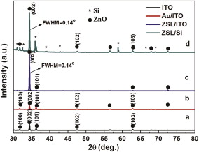 | Fig. 1 XRD patterns for ZNRs electrodeposited on varying substrates (* and • denote Si and ZnO, respectively). Electro-deposition conditions: the electrolyte consists of 0.025 mol/l Zn(NO3)2· 6H2O and 0.025 mol/l HMT. Reaction temperature: 92 ° C, current density: − 0.5 mA/cm2, reaction time: 90 min. |
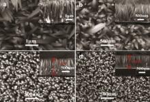
To check the effect of the substrates on the morphology and size of ZnO nanorods, four products on the series of ITO, Au/ITO, ZSL/ITO and ZSL/Si substrates were examined by SEM. The typical plan-view SEM images for four ZNRs films are displayed in Fig. 2. The insets in upper right corner in Fig. 2 show the corresponding cross-sectional images. In Fig. 2(a), the ZnO nanorods show smooth and clean surface, and have the hexagonal cone-like structure. It is seen that the ZnO nanorods are irregularly aligned on ITO glass substrate with diameters of 200-400 nm and average thickness of about 2 μ m. In Fig. 2(b), the surface morphology of the ZnO nanorods on Au/ITO substrate is similar to those nanorods on ITO glass substrate. The small area of vertically-aligned ZnO nanorods forms on the Au/ITO substrate with diameters of 150-300 nm and average thickness of about 1.5 μ m (Fig. 2(b)). However, for the ZSL modified ITO and Si substrates (Fig. 2(c and d)), it is clearly seen that the large area of vertically-aligned ZNR arrays forms on entire ZSL/ITO and ZSL/Si substrates. Especially, for the ZSL/Si substrate, almost all of ZnO nanorods are vertically-aligned on substrate with an average diameter of 30 nm. Here, the ZSL provided an active center for nanocrystal growth, so homogeneously aligned ZNR arrays were easily synthesized.
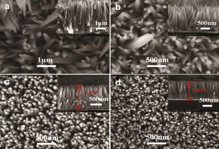 | Fig. 2 Plan-view SEM images of ZNRs electrodeposited on varying substrates: (a) ITO, (b) Au/ITO, (c) ZSL/ITO, (d) ZSL/Si. Electro-deposition condition is the same as Fig. 1. |
The morphologies of ZNRs films should be related to the lattice mismatch between the ZnO nanomaterial and substrate, and the defects of the substrate surface, and are also related to the chemical absorption, nucleation and growth[16], [17] and [18]. The appropriate lattice mismatch between the ZnO and the ITO (or Si) substrate could reduce the crystalline nuclear size and increase the nuclear number, which was beneficial to the formation of ZNR arrays[23]. Thus, the ITO (or Si) substrate was more suitable for the regular growth of ZNRs. Low growth temperature was also beneficial to the growth of ZNRs on ITO (or Si) substrate, because the lattice stress between the ZnO nanorods and the ITO (or Si) substrate was reduced substantially with decreasing growth temperature[24].
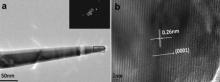
Further structural characterizations for the ZNR arrays on ZSL/Si substrate were performed by TEM and HRTEM, as shown in Fig. 3(a and b). Fig. 3(a) shows the low-resolution TEM image of an individual ZNR with an average diameter of 30 nm. The SAED pattern of the corresponding ZNR (inset at upper right corner of Fig. 3(a)) can be indexed to be the wurtzite structure of the ZnO, and indicates its single-crystal nature and its growth direction along [0001]. The HRTEM image, taken from the area marked with the black frame in Fig. 3(a), is illustrated in Fig. 3(b). The crystal lattice fringes are clearly detected and the average distance between adjacent lattice planes is 0.26 nm, corresponding well to the interplanar distance of the (0001) crystal planes of wurtzite ZnO, which further confirms that ZNR arrays prepared in ZSL/Si substrate grow along c-axis. This is also in agreement with that of XRD patterns.
 | Fig. 3 TEM, SAED and HRTEM images of ZNRs on the ZSL/Si substrates. Electro-deposition condition is the same as Fig. 1. |
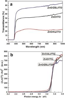
To further check the correlation of the crystalline quality with the optical transmittance in ZnO nanorods, the optical transmittance spectra of the ZNR arrays and ZnO hexagonal cone nanorods are displayed inFig. 4(a). Correspondingly, the Fig. 4(b) displays the plot of (− ln(T)· hv)2 vs photon energy of the as-electrodeposited films composed of cone ZnO nanorods and the ZNR arrays. From Fig. 4(a), it is clearly seen that the as-electrodeposited ZNR arrays on the ZSL/ITO substrate exhibit a good optical transmittance (above 80%) in visible wavelength range, and a sharp absorption in the UV region. Compared with the ZNR arrays, the cone ZnO nanorods films (on ITO and Au/ITO substrates) display a low optical transmittance of 50% and 25% in visible range, respectively, as shown in Fig. 4(a). This difference in optical transparency can be ascribed to the possible light scattering dependent on the surface regularity. The ZNR arrays are highly oriented and vertically-aligned on entire ZSL/ITO substrate, which have a nearly uniform diameter, thus, ZNR arrays exhibit a low light scattering and a good optical transparency.
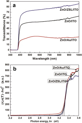 | Fig. 4 Optical transmittance spectra of ZnO cone-like nanorods (on ITO and Au/ITO), and the ZNR arrays on ZSL/ITO substrates (a); plot of (− ln(T)· hν )2 vs photon energy of the ZnO cone-like nanorods and the ZNR arrays (b). |
The electrodeposited ZnO nanostructures exhibit a band gap between 3.3 and 3.55 eV, depending on the morphology characteristic and crystal defects. ZnO, being a direct band gap semiconductor, has an absorption coefficient which obeys the following photon energies: α hν = β (hν − Eg)1/2 [25], where β is a constant, α is the absorption coefficient (per centimeter) and hν (electron volt) is the energy of excitation. The absorption coefficient α can be obtained by α = − ln(T)/d, where T is the transmittance and d is the thickness of film. Here, to estimate the band gap energy of Eg, three ZNR arrays films employed have the thickness of about 1 μ m. During the estimating on Eg, the thickness effect on the estimate of Eg was negligible. Thus, one supposed the absorption coefficient α ∝ − ln(T) in fundamental absorption region, and the better linearity was observed from the plot of (− ln(T)· hν )2 vs hν ( Fig. 4(b)). Extrapolating the plot of (α hν )2 vs hν to the x-axis, we deduced the band gap of ZNR arrays on ZSL/ITO substrate to be 3.30 eV or so, which approaches to that of the ZnO single-crystal [26]. For cone ZnO nanorods films on the ITO and Au/ITO substrates, their optical band gaps red-shift to 3.27 eV, which could be ascribed to the non uniform morphologies and crystal defects in ZnO nanostructures.
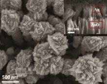
Importantly, the rapid synthesis of ZNR arrays could provide the feasibility for preparation of SERS (surface enhanced Raman scattering) nanocomposite within a shorter time by a subsequent electrochemical etching. The ITO substrate covered with ZnO nanorods was used as a working electrode, and the graphite sheet was served as a counter electrode for second-step electrodeposition process in the fresh chloroauric acid (HAuCl4) solution. Fig. 5 shows the plan-view SEM image of the hierarchical nanostructure of Au/ZNRs/ITO along the zone-axis of the ZNRs. Above experimental results proved that the ZNR arrays can be selectively etched into hierarchical nanostructures by subsequent electrochemical process. All in all, the study on synthesis of the ZNRs via a ZSL-assistant electrodeposition is of great significance for formation of the hierarchical ZnO nanostructures.
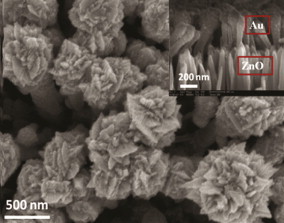 | Fig. 5 Plan-view SEM of the SERS nanocomposite prepared based on the ZNRs decorated with Au by electrodeposition process. |
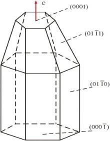
Crystal growth behavior mainly depends on the crystal inner structure that can be affected by external factors, such as temperature, concentration and time[27]. ZnO is a polar crystal, its polar axis is c-axis, and the space group is 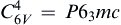


 | Fig. 6 Ideal growth model of the ZnO crystal with hexagonal wurtzite phase. |
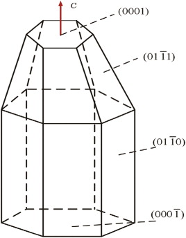
Fig. 7 shows the schematic diagrams of hexagonal ZnO nanorods formed from the electrodeposition process. The formation of ZnO can be represented as the following reactions:
equation(1)
62(CH)N42+6HO→ 36HCHO+4NH


equation(3)


Zn2+− +2OH→ 2Zn(OH)→ 2ZnO+HO

 | Fig. 7 Schematic diagrams of electrodeposition microprocess of ZNRs. |
In solution, hexamethyleneimine (HMT, (CH2)6N4) underwent hydrolysis and generated NH3 (Eq. (1)), then NH3 again underwent hydrolysis and generated OH− (Eq. (2)), and cathodic reduction of nitrate ions liberated hydroxide ions in the vicinity of the cathode (Eq. (3)). Then, zinc ions combined with hydroxyl anions (Eq. (4)). Subsequently, zinc hydroxide spontaneously dehydrated into ZnO (Eq. (4)), and Zn2+ of the zinc nitrate and OH− reacted to generate Zn(OH)2. Zn(OH)2 generated ZnO after dehydration. Since the growth of ZnO crystal was anisotropic, most of them were selectively growth along the c-axis direction. The formation of ZnO nanorods belonged to the hexagonal wurtzite structure, and its positive polar (0001) and negative polar (000 


The large-scale of ZNR arrays have been synthesized on the seed-layer modified and freed Si and ITO substrates from the aqueous solution of 0.025 mol/l Zn(NO3)2· 6H2O containing HMT during the electrodeposition process. For the ZSL/ITO and ZSL/Si substrates, the electrodeposited ZNR arrays possess a high-quality single-crystal wurtzite structure, which are vertically-aligned to the substrate surface. Optical transmittance spectra show that the ZNR arrays on ZSL/ITO substrate exhibit a high transmittance (80%) in visible wavelength range and the band gap energy red-shifts to 3.30 eV. The vertically-aligned ZNRs from the ZSL-assisted electrodeposition can effectively improve photocatalytic property of the ZnO nanorods, moreover, such ZNRs are of great significance for formation of the hierarchical ZnO nanocomposite.
The authors have declared that no competing interests exist.
| [1] |
|
| [2] |
|
| [3] |
|
| [4] |
|
| [5] |
|
| [6] |
|
| [7] |
|
| [8] |
|
| [9] |
|
| [10] |
|
| [11] |
|
| [12] |
|
| [13] |
|
| [14] |
|
| [15] |
|
| [16] |
|
| [17] |
|
| [18] |
|
| [19] |
|
| [20] |
|
| [21] |
|
| [22] |
|
| [23] |
|
| [24] |
|
| [25] |
|
| [26] |
|
| [27] |
|
| [28] |
|