
Mo6+ Modified (K0.5Na0.5)NbO3 Lead Free Ceramics: Structural, Electrical and Optical Properties
[Rani Jyoti1 , Patel Piyush Kumar1 , Adhlakha Nidhi1 , Singh Hemant1 , Yadav K.L.1, *  , Prakash Satya
2 ]
, Prakash Satya|
|


Lead free polycrystalline ceramics (K0.5Na0.5)Nb(1-
Lead zirconium titanate (PZT)-based materials are of substantial interest due to their potential applications such as high dielectric capacitors, random access memories, transducers and electro-optic devices etc [1]. Lead oxide is the main constituent of PZT-based material which is detrimental for environment as well as for living beings. Therefore, a great attention has been given to the lead free ceramics, such as Bi0.5Na0.5TiO3 (BNT)-based ceramics, BaTiO3-based ceramics, BiFeO3-based ceramics, (K,Na)NbO3-based ceramics [2], bismuth-layered structure ceramics [3] and [4] and tungsten bronze-type ceramics [5] etc. Among them, potassium sodium niobate (K0.5Na0.5NbO3) (KNN) has been proposed as a promising candidate because of its high Curie temperature, good ferroelectric and piezoelectric properties [6], [7] and [8]. KNN belongs to the perovskite orthorhombic system with a space group Amm2. It is a solid solution of ferroelectric potassium niobate (KNbO3) having Curie temperature of ∼435 °C and antiferroelectric sodium niobate (NaNbO3) with Curie temperature of ~355 °C [9]. The composition K/Na = 50/50 which is close to the morphotrophic phase boundary, has been reported to exhibit a moderate dielectric constant and an optimum piezoelectric response [10].
Different techniques like spark plasma and high energy milling [11] and [12] etc. are being used to overcome the alkali evaporation during high temperature synthesis of KNN. Chemical modification by using various dopants such as Li+, Mg2+, Ca2+, Sr2+, Ba2+, La3+, Ta5+, Ga3+ and Fe3+ etc. [10], [13], [14], [15], [16] and [17] at A or B site or by making its solid solution with LiNbO3, SrTiO3 and BaTiO3 etc. [18], [19] and [20] have been used to improve its dielectric and electrical properties. Method of synthesis has a marked influence on density and electric properties of KNN. Liu et al. [21] reported higher density and dielectric constant for KNN, when its pellets were buried in calcined KNN powder during sintering, as compared to bare KNN pellet. These changes arise due to difference in concentration and type of oxygen vacancies that increase with increasing Na/K evaporation. Since grain, grain boundary and electrode–specimen interface are contributed to the electrical properties of polycrystalline specimens, impedance spectroscopy may be used as a tool to distinguish the contributions of these effects. The output response of the impedance measurement when plotted in a complex plane appears in the form of successive semicircles representing electrical phenomenon due to grain, grain boundary effect and interfacial polarization [22] and [23]. Using elemental substitution, one can tailor the properties of the ceramics for any specific application. Till now, there are few studies on optical behaviour of pure and doped bulk KNN ceramics. Molybdenum oxides (MoO3) are one of the most attractive metal oxides due to their optical characteristics. Many reports are available regarding the optical properties of MoO3 [24], [25], [26] and [27]. Application of Mo6+ as a dopant for KNN ceramics has not yet been reported. So an attempt has been made for Mo6+ doping in KNN at Nb5+ site, with a hypothesis that Mo6+ may improve the optical properties and give rise to a system with soft characteristics as already established in the case of donor doped PZT ceramics [28] and [29]. The influence of doping on the structural, dielectric, complex impedance and optical properties of KNN ceramic has been discussed in this paper.
Polycrystalline ceramics of (K0.5Na0.5)Nb(1- x)Mo xO3 ( x = 0, 0.02, 0.04, 0.06, and 0.08) were synthesized by solid state reaction method. The chemicals Na2CO3 (Qualigns, 99.9%), K2CO3 (Himedia, 99%), Nb2O5 (Himedia, 99.9%), MoO3 (Himedia, 99.5%) were used as received. For the synthesis of (K0.5Na0.5)Nb(1- x)Mo xO3 ( x = 0, 0.02, 0.04, 0.06, and 0.08), analytical grade of above mentioned chemicals was taken in appropriate proportion and mixed thoroughly in acetone media for better mixing. Approximately 5 wt% of K2CO3 and Na2CO3 were initially added in excess to compensate for K and Na loss during calcination and sintering process. These mixed powders were calcined in air at 825 °C for 4 h. The heating rate of the furnace was set at 5 °C/min. The calcined powders were finally grounded and characterized by using an X-ray powder diffractometer (Brueker D8 Advance) with Cu Kα radiation in the angle range of 20° ≤ 2 θ ≤ 60° at a scanning rate of 1° min-1. The calcined powders were pressed using a hydraulic press into pellets of diameter 9–10 mm and thickness 0.9–1.2 mm by applying pressure of ∼6 × 10⁷ kg/m2. The pellets of x = 0 and x = 0.02 compositions were sintered at 1115 °C for 2 h but for other concentrations of Mo6+, the sintering was done at lower temperature, i.e. 1080 °C for 2 h in an air atmosphere to prevent melting of the samples. The melting temperature of MoO3 is low (~795 °C) and for higher concentration of Mo6+ this causes melting of samples. These sintered pellets were coated with high purity silver paint on two parallel surfaces and then dried at 250 °C for 30 min before performing electrical measurements. The capacitance and impedance measurement of the samples at different frequencies and temperatures were carried out using HIOKI 3532-50 LCR meter. Morphological analyses of the ceramic pellets were done by field emission scanning electron microscopy (FE-SEM, FEI quanta 200F) operating at 20 kV. The estimated optical band gap energy of the compounds was calculated with the help of UV–Vis diffuse reflectance spectrophotometer (Shimadzu UV-2450) in the wavelength range of 200–800 nm using BaSO4 as the reference. The photoluminescence analysis was conducted by using a fluorescence spectrophotometer (Hitachi F-4600) at room temperature. The powder samples were dispersed in Millipore® water to measure the photoluminescence (PL) spectra.
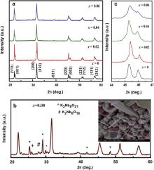
Fig. 1(a) shows the X-ray diffraction (XRD) patterns of (K0.5Na0.5)Nb(1- x)Mo xO3 ( x = 0, 0.02, 0.04 and 0.06) ceramics. The observed peaks indicate the formation of pure perovskite phase for pure and Mo6+ doped KNN up to x = 0.06. This is the clear indication for the formation of a homogenous solid solution, in which Mo6+ ion has diffused into KNN lattice. Further increasing the Mo6+ to 8 mol% in KNN, impurity phases appear as seen in Fig. 1(b). The impurity phases were identified as K2Nb8O21 and K2Nb6O16 (* and # marked, respectively) which were further matched with international center for diffraction data (JCPDS) with file Nos. 31-1060 and 28-0788, respectively. The formation of secondary phases indicates that the solubility limit of Mo6+ in the lattice of KNN has reached 6 mol% of Mo6+.
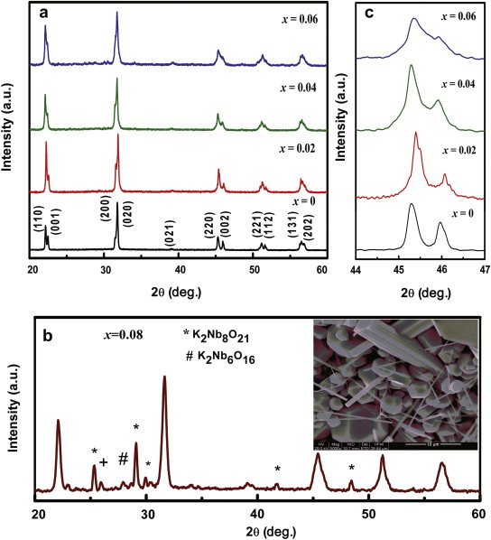 | Fig. 1. (a) XRD patterns of the (K0.5Na0.5)Nb(1- x)Mo xO3 ( x = 0, 0.02, 0.04 and 0.06), (b) XRD pattern for x = 0.08 with FE-SEM micrograph in inset, (c) merging of peaks (202) and (020). |
XRD pattern ( Fig. 1(b)) and FE-SEM micrographs (inset of Fig. 1(b)) of x = 0.08 composition show a large amount of impurity phases. Due to appearance of impurity phase, further study was not carried out for this composition.
The enlarged view of XRD pattern for (K0.5Na0.5)Nb(1- x)Mo xO3 ( x = 0, 0.02, 0.04 and 0.06) in the angle range from 44° to 47° is shown in Fig. 1(c). It depicts that the two diffraction peaks (202) and (020) start to merge into a single peak with increasing concentration of Mo6+. This indicates that the ceramics have a tendency to transform into another phase, e.g. pseudocubic, as the concentration of Mo6+ increases.
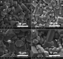
Fig. 2 shows the FE-SEM micrographs of (K0.5Na0.5)Nb(1- x)Mo xO3 ( x = 0, 0.02, 0.04 and 0.06) sintered ceramics. All the micrographs show cuboidal shaped grains. There is no much change in grain size or shape on Mo6+ doping up to x = 0.06. The average grain sizes of the compounds were calculated by linear intercept method and found to be in the range of ~5–7 μm.
 | Fig. 2. FE-SEM photographs of (K0.5Na0.5)Nb(1- x)Mo xO3: (a) x = 0, (b) x = 0.02, (c) x = 0.04, (d) x = 0.06. |
The variation of dielectric constant ( ɛ) with temperature for (K0.5Na0.5)Nb(1- x)Mo xO3 ( x = 0, 0.02, 0.04 and 0.06) ceramics at frequency 1 kHz is shown in Fig. 3(a). This depicts that pure KNN undergoes two types of phase transitions: (i) orthorhombic to tetragonal transition ( TO–T) at 200 °C and (ii) tetragonal to cubic phase transition ( TC) at 395 °C. Mo6+ doped samples also exhibit similar phase transitions with different TO–T and TC. There is no systematic change in TO–T but TC shifted slightly towards low temperature side from 395 to 380 °C with increasing concentration of Mo6+. The dielectric constant decreases with broad dielectric peak at TC as the concentration of Mo6+ increases. This broadening may be due to compositional fluctuation. Fig. 3(b) shows the dielectric loss of (K0.5Na0.5)Nb(1- x)Mo xO3 ( x = 0, 0.02, 0.04 and 0.06) as a function of temperature at frequency 1 kHz. The dielectric loss at room temperature varies in the range of ~0.035–0.055 for x = 0–0.06 Mo6+ concentration.
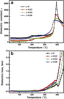 | Fig. 3. Variation of: (a) dielectric constant (ɛ), (b) dielectric loss (tan δ) of (K0.5Na0.5)Nb(1- x)Mo xO3 ( x = 0, 0.02, 0.04 and 0.06) with temperature at frequency 1 kHz. |
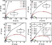
The analysis of complex impedance ( Z*) can give information of the frequency dependent properties of materials. The value of Z* can be evaluated as follows:
where and
and are the real and the imaginary part of Z*, Rsand Csis the resistance and capacitance in series, respectively, ω= 2π fis the angular frequency and j=
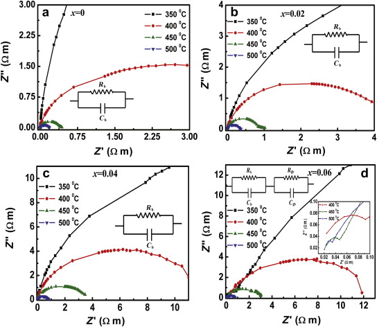 | Fig. 4. Complex impedance spectra of (K0.5Na0.5)Nb(1- x)Mo xO3 at temperatures of 350, 400, 450 and 500 °C for: (a) x = 0, (b) x = 0.02, (c) x = 0.04, (d) x = 0.06. |
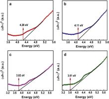
Fig. 5 shows the diffuse reflectance spectra of (K0.5Na0.5)Nb(1- x)Mo xO3 ( x = 0, 0.02, 0.04 and 0.06) ceramics for the determination of optical band gap of the compounds. The band gap energy is determined by the use of Kubelka–Monk (KM) formalism [34] and [35]:
where Ris experimental reflectance. Within the energy range containing the absorption edge features, F( R) can be assumed to be proportional to the absorption coefficient ( α) [34] and [36]. The optical band gap energy ( Eg) value can be evaluated with the help of fundamental absorption, which corresponds to electron excitation from the valence band to conduction band. The relation between the absorption coefficient ( α) and the incident photon energy ( hν) for the direct band gap is as follows:

where his the Planck constant, νis the frequency, αis the absorbance coefficient, Ais a constant, Egis the optical band gap energy. The extrapolation of linear part of (α hν)2vs ( hν) curves to the x-axis provides the band gap energy. In KNN, the band gap corresponds to the transition from the top of the valence band occupied by O2 pelectron state to the bottom of the conduction bands dominated by the empty Nb4 delectron states [37]. The value of band gap energy of KNN was found to decrease with increasing concentration of Mo6+. The band gap energy for (K0.5Na0.5)Nb(1- x)Mo xO3( x= 0, 0.02, 0.04 and 0.06) were found to be 4.28, 4.11, 3.82 and 3.61 eV, respectively. One of the reasons for this decrease in band gap energy is that the band gap energy of the bulk MoO3is low (~2.9 eV) [24], therefore with increasing concentration of Mo6+the band gap energy of KNN decreases. Another reason of this red shift in band gap energy of KNN may be attributed to structural modification, which is also confirmed by XRD pattern. Generally in ABO3-type perovskite compounds, the optical properties are mainly determined by the oxygen-octahedral structure [38]. In Mo doped KNN, the oxygen-octahedral may shrink due to smaller radius of Mo+6than that of Nb+5which may be responsible for red shift in band gap energy. Therefore band gap of KNN can be tuned with Mo+6doping.
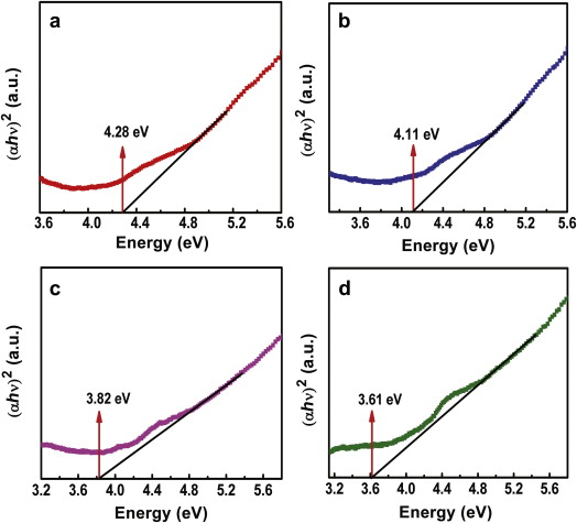 | Fig. 5. Plot of ( αhν)2 vs hν for the (K0.5Na0.5)Nb(1- x)Mo xO3 at room temperature: (a) x = 0, (b) x = 0.02, (c) x = 0.04, (d) x = 0.06. |
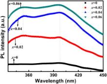
For further study of optical property of pure as well as Mo+6 doped KNN ceramics, photoluminescence spectroscopy was used. Room temperature photoluminescence (PL) spectra of (K0.5Na0.5)Nb(1- x)Mo xO3 for x = 0, 0.02, 0.04 and 0.06 in the wavelength range of 335–450 nm are shown in Fig. 6. The suspension of powder samples was excited by photons of wavelength 300 nm. One emission band ∼397 nm in visible region (violet emission) was observed for pure KNN. For Mo+6 doped (K0.5Na0.5)Nb(1- x)Mo xO3 ( x = 0.02, 0.04, and 0.06), another emission band was also observed in UV region (∼354 nm) along with visible band around ∼397 nm. The appearance of emission band ∼354 nm in Mo+6 doped KNN may be attributed to the presence of Mo+6 ions because MoO3 shows PL at room temperature [24] and [25]. Similar type of emission has already been reported by Navas et al. [24] in MoO3 film. There are many reports on the appearance of PL spectra due to doping of various elements [39] and [40]. The presence of near band UV emission in doped sample (∼354 nm) may be ascribed to exciton recombination that is the recombination of electrons in conduction band and holes in valence band. The electron hole recombination occurs during inelastic exciton–exciton collision [41]. Presence of visible emission band may be ascribed to the transitions of excited optical centres in the deep levels. The deep level emission is usually attributed to the presence of impurities and defects [24]. This photoluminescence behaviour of (K0.5Na0.5)Nb(1- x)Mo xO3 ceramics may lead to its application in optical devices.
 | Fig. 6. Room temperature photoluminescence spectra of (K0.5Na0.5)Nb(1- x)Mo xO3 for x = 0, 0.02, 0.04 and 0.06. |
Polycrystalline (K0.5Na0.5)Nb(1- x)Mo xO3 have been synthesized by solid state reaction method. There is a change in phase into another phase, i.e. pseudocubic, as the concentration of Mo6+ increases in KNN. Mo6+ ions are found to have limited solubility upto 6 mol% in the host compound KNN. Further increasing the Mo6+ to 8 mol% leads to the formation of impurity phases. The impedance analysis reveals mainly grain contribution upto 4 mol% whereas for 6 mol% of Mo6+ the grain boundary contribution is also observed. The red shift in the band gap energy is observed with increasing concentration of Mo6+ in KNN. Interestingly, near band edge UV emission has been seen in Mo6+ doped KNN along with visible emission band of pure KNN in photoluminescence spectra at room temperature.
Acknowledgements
Authors acknowledge the financial support from Council of Scientific and Industrial Research, New Delhi India under the research Grant No. 03(1156)/10/EMR II.
| 1. |
|
| 2. |
|
| 3. |
|
| 4. |
|
| 5. |
|
| 6. |
|
| 7. |
|
| 8. |
|
| 9. |
|
| 10. |
|
| 11. |
|
| 12. |
|
| 13. |
|
| 14. |
|
| 15. |
|
| 16. |
|
| 17. |
|
| 18. |
|
| 19. |
|
| 20. |
|
| 21. |
|
| 22. |
|
| 23. |
|
| 24. |
|
| 25. |
|
| 26. |
|
| 27. |
|
| 28. |
|
| 29. |
|
| 30. |
|
| 31. |
|
| 32. |
|
| 33. |
|
| 34. |
|
| 35. |
|
| 36. |
|
| 37. |
|
| 38. |
|
| 39. |
|
| 40. |
|
| 41. |
|