
Plasmon-enhanced Performance of Dye-sensitized Solar Cells Based on Electrodeposited Ag Nanoparticles
[Luan Xinning, Wang Ying*  ]
]
]
|
|


In the present work, pulse current deposition is used to deposit evenly distributed and uniformly sized Ag nanoparticles onto a TiO2 nanotube array as photoelectrode in dye-sensitized solar cells (DSSCs), and the size and amount of loading Ag nanoparticles are controlled by the pulse deposition time. Due to the enhanced light absorption and electron–hole separation caused by plasmon effect, DSSCs based on Ag-modified TiO2 nanotube arrays show higher energy conversion efficiencies than those based on bare nanotubes with the same tube length. Particularly, DSSC based on nanotubes modified using pulse deposition time 1 s/3 s delivers the highest energy conversion efficiency of 1.68% and the largest short-circuit current of 4.37 mA/cm2, while DSSC consisting of bare nanotubes exhibits efficiency of 1.20% and short-circuit current of 2.27 mA/cm2, which represents a 40% enhancement of cell efficiency in DSSC based on Ag-modified TiO2 nanotubes. It is also noted that overly long pulse deposition time will not further increase DSSC efficiency due to agglomeration of Ag particles. For example, when the pulse deposition time is increased to 2 s/6 s, DSSC based on Ag-modified nanotubes exhibits a lower efficiency of 1.42%. Moreover, high-concentration TiCl4 treatment on TiO2 nanotube arrays can further increase the energy conversion efficiencies to 3.82% and 2.61% for DSSC based on Ag-modified TiO2 nanotubes and DSSC based on bare TiO2 nanotubes, respectively, by significantly creating more surface area for dye loading.
New generations of solar cells have emerged, as conventional silicon solar cells with high energy conversion efficiencies pose challenges of complicated and high-cost processing and production [1] and [2]. Dye-sensitized solar cells (DSSCs) have attracted increasing attention for their easy processing and low cost, since mesoporous titania with high surface area was used as photo-anode to improved energy conversion efficiency of DSSC as reported by Grätzel et al. in 1991 [3], [4], [5], [6], [7], [8], [9], [10], [11] and [12]. In a DSSC, electrons of dye molecules are excited by solar energy absorption and then the electrons from the photo-excited dye inject into the conduction band of photo-anode such as titanium dioxide (TiO2). The electrons then diffuse through TiO2 layer to the electrode and subsequently reach the counter electrode through an external circuit. The dye molecules regain electrons from a redox couple iodide/triiodide (I-/I3-) in an electrolyte. The iodide is regenerated in turn by the reduction of triiodide at the counter electrode, and this process requires a catalytic functionality of Pt on the cathode surface.
TiO2 is commonly used as photo-anode material in current DSSCs. One-dimensional TiO2 nanostructures such as TiO2 nanotube arrays have attracted much attention as the photo-anode material in DSSCs due to their ordered vertical structure which facilitates filling of new sensitizer molecules or non-volatile electrolytes for improved efficiency and stability of DSSCs, while conventional mesoporous TiO2 film has a disordered structure that makes infiltration of larger sensitizer molecules or viscous electrolytes difficult and ineffective [13], [14], [15], [16], [17], [18], [19], [20], [21] and [22]. However, DSSC based on TiO2 nanotube array exhibits limited energy conversion efficiency owning to its lower surface area than mesoporous TiO2 film [23], [24], [25] and [26].
Numerous approaches and strategies have been investigated so as to enhance photoelectric conversion efficiency of DSSC by surface modification with noble metal [27], [28] and [29], using semiconductor quantum dots [30] and [31], developing new dyes [32], [33] and [34], and designing new morphology [35], [36] and [37]. The purposes of these methods are to either increase the surface area for dye loading or increase the light harvesting ability and/or suppress the recombination of photogenerated electron–hole pairs. Among these approaches, surface modification by noble metal has been considered as a very effective approach to enhance energy conversion efficiency of DSSC by improving its light harvesting. Surface plasmon induced by noble metals has the potential for enhancing the optical absorption. The surface plasmon effect is caused by light-driven collective oscillations of conduction electrons in metallic nanoparticles. The nanoparticles must be smaller than the wavelength of exciting light for electrons to oscillate with the electric field of light. When these conditions are met, an enhanced electromagnetic field is found nearby the surface of nanoparticle. The enhanced electromagnetic field is highly dependent upon the wavelength of incident light, as well as the shape, size and aggregation state of the nanoparticle. Atwater et al. [38] recently outlined three types of plasmonic light-trapping geometries for incorporating metal nanoparticles: i) Far-field scattering. When light is scattered from noble metal nanoparticles in DSSC, light is preferentially scattered and trapped into the semiconductor by multiple and high-angle scattering, causing an increase in the effective optical path length in the cell. ii) Near-field scattering. When the wavelength of the irradiation sources is correlated with the optical absorption of the surface plasmon resonance, an increase in local electromagnetic field is found nearby metal surface. The photo-excited particles' near-field causes the creation of electron–hole (e–h) pairs in semiconductor and suppresses the recombination of electrons in dye and/or electrolyte. iii) Surface plasmon polaritons at the metal/semiconductor interface. A corrugated metallic film on the back of semiconductor can couple sunlight into surface plasmon polaritons at metal/semiconductor interface. Therefore, utilization of plasmon effect for enhancement of light is a promising procedure for improving the efficiency of DSSC.
Till now, surface plasmon arising from metal nanoparticles has mostly been applied to increase optical absorption and/or photocurrent in the field of silicon solar cells [39], [40], [41] and [42] and organic solar cells [43] and [44]. Not many examples of this concept have been introduced and demonstrated in DSSCs. Considering plasmon effect of various noble metals, Ag is one of the most suitable candidates for practical applications due to its easy preparation and lower cost than others. Several methods have been reported to deposit Ag nanoparticles onto TiO2 such as photo-induced deposition, calcination reduction, and electrochemical deposition. However, none is able to prevent the aggregation of Ag particles and keep structures uniform during the deposition process. Chou et al. synthesized TiO2/Ag composites via dry coating process and investigated their applications in DSSCs [45]. Such a nano-metal modified DSSC yielded a photo conversion efficiency of 0.93%, which was higher than DSSC based on unmodified nanotubes (0.71%) with identical film thickness of 8.0 μm. However, this efficiency of 0.93% was still low, which was ascribed to agglomeration of Ag nanoparticles and a wide particle size distribution of 20–100 nm. Agarwala et al. [46] also prepared Ag nanoparticles onto TiO2 nanotubes by using a photo reduction method, to scatter light and generate surface plasmon effect. The DSSC efficiency was enhanced by 22% after being modified with Ag nanoparticles. However, the particle size was larger than 70 nm and the nanoparticles were mixed with some rod like structures, resulting in lower dye absorption and less scattering effect. On the other hand, Lai et al. developed a simple method using pulse current (PC) deposition to deposit uniformly distributed spherical Ag nanoparticles (2–10 nm) on the surface of prepared TiO2 nanotube arrays. The generated photocurrent was found to be 36% higher than that of randomly distributed Ag particles prepared by photocatalytic reduction [47]. PC electrodeposition is considered as a facile method for controlling the electrocrystallization process and hence depositing materials with unique structures and properties. By tuning current-on time ( ton) and current-off time ( toff), instantaneous current density applied by pulse control can lead to ultrafine-grained structures and homogeneous surface appearance of the deposit. Therefore, PC electrodeposition can form evenly distributed and uniformly nano-sized Ag. On the other hand, direct current (DC) electrodeposition results in inhomogeneous Ag with rough surface; hence, it is not a suitable method for producing Ag nanoparticles [48].
As summarized above, size of Ag nanoparticles synthesized via photo reduction deposition method is too large and uncontrollable; as a result, these commonly-used methods are not suitable choices for enhancing plasmon effect in DSSCs. However, the enhancement of plasmon effect can be easily achieved by using pulse current deposition method, which can produce evenly distributed nanoparticles with controllable size distribution by tuning pulse current. However, this method has never been used for depositing metallic particles for plasmon effect in DSSCs. The present work is the first effort to employ pulse current deposition method for enhancing plasmon effect in DSSCs. TiO2 nanotube arrays are prepared via anodization and followed by deposition of uniformly distributed spherical Ag nanoparticles via pulse current deposition. This process is easy to implement and can effectively suppress the agglomeration of Ag particles by taking advantage of high nucleation rate of Ag under the PC condition. DSSCs based on Ag-modified TiO2 nanotube arrays show significantly enhanced performance than DSSCs consisting of bare TiO2 nanotube arrays. Efficiency of such DSSCs can also be maximized by tuning pulse deposition time of Ag nanoparticles. Moreover, efficiency of DSSCs can be further improved by treating TiO2 nanotubes with high concentration TiCl4 prior to Ag deposition.
Ti foils (0.25 mm thickness, 99.5 wt% purity, Alfa Aesar) were degreased by sonicating in acetone, deionized (DI) water, and ethanol for 15 min, respectively, then rinsed with ethanol and dried in a nitrogen stream. Electrochemical anodization of the Ti foils was carried out in a two-electrode cell, with a platinum mesh as the counter electrode at room temperature. The electrolyte for anodization was prepared with anhydrous ethylene glycol (EG) with NH4F (0.3 wt%) and H2O (5 vol%). The voltage was supplied by a DC power supply with a digital display (Model 1623A, PK Precision). After anodization, the samples were rinsed in deionized water (DI water) and dried in air, followed by heat treatment at 450 °C in air for 3 h to produce anatase phase. Optional TiCl4 treatment was performed on TiO2 nanotube arrays by soaking annealed nanotube in 100 mL of 0.2 mol/L TiCl4 aqueous solution at 70 °C for 30 min and then annealing at 450 °C in air for 30 min.
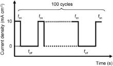
Pulse-current electrodeposition of Ag nanoparticles was carried out by immersing the as-prepared TiO2 nanotube in an aqueous electrolyte composed of 10 mmol/L AgNO3 and 100 mmol/L NaNO3 at room temperature. The TiO2 nanotube array and a platinum mesh were used as the working and counter electrodes, respectively. A pulse-current of 10 mA/cm2 with different alternating on-time and off-time (0.5 s/1.5 s, 1 s/3 s, 2 s/6 s) for 100 cycles were applied. Fig. 1 shows a scheme showing the pulse current process for electrochemical deposition of Ag nanoparticles with a rectangular pulse shape composed of an alternating on-time and off-time for 100 deposition cycles. The Ag-deposited samples were then rinsed with DI water and dried in vacuum at 50 °C overnight.
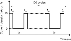 | Fig. 1. Schematic showing the pulse current process for electrochemical deposition of Ag with a rectangular pulse shape composed of alternating on-time and off-time for 100 deposition cycles. |
To fabricate DSSCs, TiO2 nanotube arrays with or without Ag modifications were soaked in anhydrous ethanol containing 0.2 mmol/L N719 dye (Ru[LL′-(NCS)2], L = 2,2′-bipyridyl-4,4′-dicarboxylic acid, L′ = 2,2′-bipyridyl-4,4′-ditetrabutyl-ammonium carboxylate, Solaronix Co.) and sensitized for 24 h at room temperature. Afterward, these dye-sensitized TiO2 nanotube arrays with an active area of approximately 0.25 cm2 were rinsed with acetonitrile in order to remove physisorbed N719 dye molecules. Platinized counter electrode was fabricated by drop casting 0.5 mmol/L H2PtCl6/isopropanol solution on FTO glass substrate that had a hole for electrolyte injection later on, followed by heating at 400 °C in air for 20 min. The dye-sensitized TiO2 nanotube arrays with or without Ag modifications were sandwiched together with Pt-coated FTO glass by using a 100 μm thick hot-melt sealing film as the spacer (Meltonix 1170-100, Solaronix Co.). DSSCs were sealed by applying heat and pressure with a hot press at 110 °C. A I-/I3- based electrolyte, which contained 0.10 mol/L GTC in a mixture of acetonitrile and valeronitrile (85:15 v/v) (No. ES-0004, IoLiTec Inc., Germany) was injected through the hole on the Pt-coated FTO into DSSC.
Crystal structure of TiO2 nanotube arrays was determined by X-ray diffraction (XRD) using a Rigaku MiniFlex diffractometer with Cu Kα radiation operated at 30 kV and 15 mA at a scan rate of 2°/min. A FEI Quanta 3D FEG scanning electron microscope (SEM) at an accelerating voltage of 5–20 kV was used to characterize the morphology of TiO2 nanotube arrays. Chemical composition of these nanotubes was studied by energy dispersive X-ray spectroscopy (EDX) on a Hitachi S-3600N SEM. Surface composition of TiO2 nanotube arrays was analyzed via an X-ray photoelectron spectroscope (XPS) on the AXIS-165 XPS (Kratos Analytical Ltd.) with an AXIS 165 spectrometer from Kratos Analytical LTD by using a twin-anode Al Kα (1486.6 eV) X-ray source. Transmission electron microscopy (TEM, JEM-1011, JEOL LTD.) with an accelerating voltage of 80 kV was used to characterize the morphology of Ag-modified TiO2 nanotubes. The current–voltage ( J– V) characteristics of DSSCs were recorded using a Keithley 2400 source meter. A solar light simulator (Model: 67005, Oriel) was used to simulate sunlight under one sun AM 1.5 G (100 mW/cm2) illumination provided by a 150 W Xenon arc lamp (Model: 6256, Oriel) and calibrated using a Si solar reference cell (Model: 91150V, Oriel). Backside illumination mode was used, since the photo-anode consists of TiO2 nanotube array on Ti substrate which was not transparent to light.
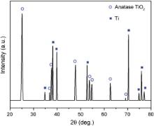
XRD analysis is utilized to examine the crystallinity of TiO2 nanotubes. Fig. 2 shows XRD patterns of bare TiO2 nanotube arrays annealed at 450 °C in air for 2 h. The peaks at 2 θ = 25.4° and 2 θ = 48.0° correspond to (101) and (200) in TiO2 anatase phase, and all of the other dominant peaks correspond to the reflection of Ti foil substrate. This result suggests that the as-prepared anodic TiO2 nanotubes convert to anatase phase after being heated at high temperatures, which can be used as photo-anodes in DSSCs.
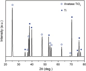 | Fig. 2. X-ray diffraction pattern of bare TiO2 nanotube array annealed at 450 °C in air for 2 h. |
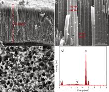
Fig. 3 shows SEM images and EDX spectrum of TiO2 nanotube arrays modified with Ag nanoparticles (NPs) via pulse deposition time of 1 s/3 s. The cross-section SEM image in Fig. 3(a) shows that the structure of TiO2 nanotube arrays preserves well after the PC deposition. Thickness of the TiO2 nanotube arrays is estimated to be ∼6.1 μm, and the average diameter of these nanotubes is ∼120 nm. It is important to note that Ag NPs are uniformly distributed and anchored along the surface of the tube structure. It is observed from Fig. 3(b) that most of Ag nanoparticles have a size in a range of 10–40 nm. The top-view SEM image in Fig. 3(c) shows Ag NPs deposited on the open entrances of TiO2 nanotube arrays. It can be seen that Ag NPs deposited on the top open entrances of TiO2 nanotubes (showing a particle size up to 60 nm) are larger than Ag NPs on the tube walls. Meanwhile, Ag NPs deposited on the top open entrances of TiO2 nanotubes are denser (without any obvious agglomeration) than Ag NPs on the tube walls. Such a larger particle size and denser distribution of Ag NPs on the top of TiO2 nanotubes are possibly due to the top open entrances of TiO2 nanotubes being more exposed to electrochemical deposition. Fig. 3(d) displays the EDX spectrum of these TiO2 nanotubes arrays modified with Ag NPs. A small amount of Ag element is detected, as evidenced by its weak but discernible peaks in the EDX spectrum.
 | Fig. 3. (a, b) Cross-sectional, (c) top-view SEM images, and (d) EDS spectrum of TiO2 nanotube arrays modified with Ag nanoparticles via pulse deposition time of 1 s/3 s. |
To further study the details about Ag NPs deposited on TiO2 nanotube arrays via pulse deposition time of 1 s/3 s, its TEM image is obtained as shown in Fig. 4. The average diameter of Ag NPs shown in the TEM image is approximately 20 nm, which is consistent with the particle size shown in the SEM images earlier. This homogeneous dispersion of Ag NPs on TiO2 nanotube arrays is desirable for efficient light harvesting, yielding high plasmon-induced activity for electron transportation.
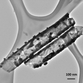 | Fig. 4. TEM image of a TiO2 nanotube modified with Ag nanoparticles via pulse deposition time of 1 s/3 s. |
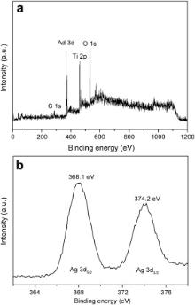
To further confirm the formation of Ag NPs from the pulse deposition, XPS is also employed to study surface composition of Ag-modified TiO2 nanotubes arrays. The XPS spectrum taken from TiO2 nanotubes arrays modified with Ag NPs via pulse deposition time of 1 s/3 s exhibits the Ag 3 d peak in Fig. 5(a). In Fig. 5(b), the peaks observed at 368.1 eV and 374.2 eV are ascribed to metallic Ag 3 d5/2 and Ag 3 d3/2, respectively, confirming metallic Ag existence on the surface of TiO2 nanotube arrays. These findings reveal that Ag-modified TiO2 nanotube arrays are successfully achieved by electrochemical deposition of Ag in AgNO3-containing solution.
 | Fig. 5. (a) XPS spectra and (b) Ag 3 d XPS peak of TiO2 nanotubes modified with Ag nanoparticles via pulse deposition time of 1 s/3 s. |
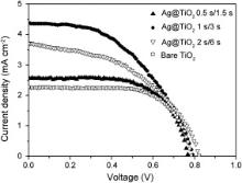
Performances of DSSCs based on bare and Ag-modified TiO2 nanotubes electrodes are examined under 1 sun AM 1.5 simulated sunlight. Fig. 6 presents J– V curves of DSSCs based on 6.1-μm-long TiO2 nanotubes arrays modified with Ag NPs using different pulse deposition time (0.5 s/1.5 s, 1 s/3 s, and 2 s/6 s). Photovoltaic characteristics of these DSSCs, such as short-circuit current ( Jsc), open-circuit voltage ( Voc), fill factor (FF), and efficiency ( η) are summarized in . It is evident that the short-circuit currents of all Ag-modified TiO2 nanotubes based DSSCs (0.5 s/1.5 s, 1 s/3 s, and 2 s/6 s) are larger than that of bare TiO2 nanotubes based DSSCs, since the Ag NPs on side walls enhance absorption and charge separation, while there are no substantial differences in the photovoltages. DSSC based on Ag@TiO2 (Ag-modified TiO2 nanotubes) synthesized via the shorter pulse deposition time of 0.5 s/1.5 s, delivers an energy conversion efficiency of 1.28%, which is just slightly higher than the efficiency (1.20%) of DSSC based on bare nanotube, possibly because the amount of Ag NPs loading is too low to show any plasmon effect. The DSSC based on Ag@TiO2 1 s/3 s (Ag-modified TiO2 via pulse deposition time of 1 s/3 s) delivers the highest energy conversion efficiency (1.68%) exhibiting Voc of 0.79 V, Jsc of 4.37 mA/cm2, and FF of 0.49, which represents a 40.0% increase in cell efficiency compared to DSSC consisting of bare TiO2 nanotube array (1.20%). In theory, the maximum voltage ( Vmax) generated by DSSC is the difference between the (quasi-)Fermi level of the TiO2 and the redox potential of the electrolyte, about 0.7 V under solar illumination conditions. Since the loaded Ag nanoparticles do not affect the Fermi level of TiO2 and redox potential of electrolyte much, Ag deposition on TiO2 would not improve Voc. The improved Jsc is resulted from higher plasmon resonance effect caused by coverage of Ag NPs on the TiO2 nanotube surface, which increases the number of photoelectrons generated and improves the effective separation of electron–hole pairs. Therefore, the loaded Ag nanoparticles can improve short-circuit current rather than the open-circuit voltage in these DSSCs. Interestingly, the efficiency of DSSC based on Ag-modified TiO2 nanotube array decreases again, as the pulse deposition time used for depositing Ag nanoparticles is increased to 2 s/6 s, due to agglomeration of Ag NPs and formation of some particles with larger size resulted from longer pulse deposition time as shown in . Such agglomeration of Ag NPs on TiO2 nanotubes results in less surface area for dye loading as well as ineffective light absorption and charge separation.
 | Fig. 6. J– V characteristics of DSSCs based on different TiO2 nanotube arrays (Ag@TiO2 0.5 s/1.5 s: TiO2 nanotubes modified with Ag nanoparticles via pulse deposition time of 0.5 s/1.5 s; Ag@TiO2 1 s/3 s: TiO2 nanotubes modified with Ag nanoparticles via pulse deposition time of 1 s/3 s; Ag@TiO2 2 s/6 s: TiO2 nanotubes modified with Ag nanoparticles via pulse deposition time of 2 s/6 s; bare TiO2: unmodified TiO2 nanotubes). |
| Table 1. Photovoltaic characteristics of dye-sensitized solar cells shown in Fig. 6</p> |
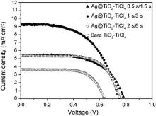
To further improve energy conversion efficiency of DSSC based on TiO2 nanotubes, treatment of TiO2 nanotubes with high concentration TiCl4 is carried out in this work. It has been reported that TiCl4 treatment can enhance dye absorption on the surface, improve the electron transport properties in nanocrystalline TiO2 films, and increase the charge separation efficiency [49], [50] and [51]. After being treated in TiCl4 aqueous solution, TiO2 nanotube arrays are sensitized with N719 dye and then integrated into DSSCs. Fig. 7 compares the J– V characteristics of DSSCs based on TiCl4 treated bare and Ag-modified TiO2 nanotubes as a function of different pulse deposition time (0.5 s/1.5 s, 1 s/3 s, and 2 s/6 s). Detailed photovoltaic performance parameters are presented in . Compared to untreated bare TiO2 nanotubes, the energy conversion efficiency of DSSC based on TiCl4 treated bare TiO2 nanotubes is increased to 2.61%, and such enhancement is mainly originated from the increased short-circuit current density. Likewise, the efficiency of DSSC based on Ag@TiO2–TiCl4 0.5 s/1.5 s (TiCl4-treated TiO2 nanotubes modified with Ag NPs via pulse deposition time of 0.5 s/1.5 s) increase to 2.56% presenting a 100% enhancement of efficiency compared to DSSC based on Ag@TiO2 0.5 s/1.5 s (1.28%). The short-circuit current density of DSSC based on Ag@TiO2–TiCl4 0.5 s/1.5 s shows slight enhancement than that of DSSC based on bare TiO2–TiCl4 and the enhancement is not significant due to small amount of Ag loading resulted from short pulse deposition time of Ag. In particular, the effect of Ag modification to enhance energy conversion efficiency is more significant for DSSC based on Ag@TiO2–TiCl4 1 s/3 s (TiCl4 treated TiO2 modified with Ag NPs via pulse deposition time of 1 s/3 s), which delivers the highest energy conversion efficiency (3.82%) with Voc of 0.75 V, Jsc of 9.27 mA/cm2 and FF of 0.55 ( ), which represents a 46.4% increase in cell efficiency compared to that of DSSC based on bare TiO2–TiCl4 (TiCl4-treated TiO2 nanotubes) nanotube array (2.61%). These results confirm that Ag NPs loaded on TiO2 nanotube surface significantly increase the performance of DSSCs.
 | Fig. 7. J– V characteristics of DSSCs based on different TiCl4-treated TiO2 nanotube arrays (Ag@TiO2–TiCl4 0.5 s/1.5 s: TiO2 nanotubes modified with Ag nanoparticles via pulse deposition time of 0.5 s/1.5 s; Ag@TiO2–TiCl4 1 s/3 s: TiO2 nanotubes modified with Ag nanoparticles via pulse deposition time of 1 s/3 s; Ag@TiO2–TiCl4 2 s/6 s: TiO2 nanotubes modified with Ag nanoparticles via pulse deposition time of 2 s/6 s; bare TiO2–TiCl4: unmodified TiO2 nanotubes). |
| Table 2. Photovoltaic characteristics of dye-sensitized solar cells shown in Fig. 7</p> |
It is, however, noteworthy that DSSC based on Ag@TiO2–TiCl4 2 s/6 s shows a large decrease in efficiency compared to DSSC based on TiCl4 treated bare TiO2 nanotubes. DSSC based on Ag@TiO2–TiCl4 2 s/6 s (TiCl4 treated TiO2 nanotubes modified with Ag NPs via pulse deposition time of 2 s/6 s) delivers a low energy conversion efficiency of 1.55% with Voc of 0.63 V, Jsc of 3.66 mA/cm2, FF of 0.67, as summarized in . It can be observed that the drastic efficiency drop of DSSCs based on Ag@TiO2–TiCl4 2 s/6 s is mainly originated from the decreased short-circuit current. The decrease of short-circuit current may be attributed to the following reasons. Long pulse deposition time (2 s/6 s) may cause agglomeration of Ag NPs on the TiO2 nanotubes surface and this effect is more distinct for TiO2 nanotubes treated with TiCl4. TiCl4 treatment yields very tiny TiO2 nanoparticles on the surface of TiO2 nanotubes ( (a and b)), some of which may partially plug the top entrances of TiO2 nanotubes ( (c)), resulting in more sites for Ag deposition. When the deposition time is very long and since the tops of TiO2 nanotubes are partially plugged and are much more exposed to electrochemical deposition than tube walls, large agglomerates of Ag NPs would form on the top of TiO2 nanotubes without much deposition of Ag NPs along tube walls ( (d–f)), leading to reduced plasmon effect and decreased surface area for dye loading. In the case of surface plasmon, metallic nanoparticles must be smaller than the wavelength of the exciting light in order for electrons to oscillate together in response to the electric field of the excitation light. Agglomerates of Ag NPs as well as those with larger particle size (more than 200 nm) are much more difficult to be excited by radical light. Another issue is that Ag agglomerates or larger Ag particles have more severe plasmon decay. The intensity of electrons transferred to TiO2 depends on the distance that plasmon travel from radical light impact position to TiO2. Vesseur et al. [52] pointed out that plasmon excited by radical light, which are emitted radially from the impact position, are lost through absorption unless they are converted to a target. Therefore, plasmon excited on the surface of TiO2 decays when transferred to the bottom of nanotube. Hence, plasmon decay is more severe in the case of Ag@TiO2–TiCl4 2 s/6 s, which has large Ag agglomerates or particles on the tops of TiO2 nanotubes and few Ag nanoparticles along the walls.
It can be seen by comparing Fig. 6 with Fig. 7 that, DSSCs based on TiCl4 treated TiO2 nanotubes show higher energy conversion efficiency than DSSCs based on untreated TiO2 nanotube, due to larger surface area of TiO2 nanotube resulted from TiCl4 treatment. It can also be observed that the effect of Ag NPs to improve energy conversion efficiency and short-circuit current is more distinct for DSSCs based on Ag@TiO2–TiCl4 1 s/3 s than DSSCs consisting of TiO2 nanotubes modified with Ag via other shorter or longer pulse deposition time, because this pulse deposition time (1 s/3 s) yields evenly-distributed and uniformly-sized Ag nanoparticles, leading to enhanced surface plasmon resonance and subsequent improved optical absorption. The particle size of Ag NPs synthesized via commonly-used methods such as photo reduction deposition methods is too large and uncontrollable, while pulse current deposition can provide uniformly distributed nanoparticles which are necessary for plasmon effect in DSSC.
In summary, TiO2 nanotube arrays are synthesized by anodizing Ti foils in EG electrolytes with a small amount of NH4F and H2O under alternating-voltage conditions, and subsequent heat treatment transforms them to anatase phase for modification with Ag nanoparticles via electrochemical deposition, for enhanced efficiencies of DSSCs. Ag nanoparticles with a size distribution up to 10–40 nm are formed on the side walls of TiO2 nanotubes. Metallic Ag formation is confirmed by EDS and XPS analyses. In addition, the loading amount of Ag nanoparticle can be easily optimized by adjusting pulse deposition time. Most of DSSCs based on Ag-modified TiO2 nanotube arrays show significantly higher energy conversion efficiencies than DSSC consisting of bare nanotube array of the same length. Such enhancement is ascribed to the surface plasmon resonance induced by uniformly deposited Ag NPs. Increasing the Ag deposition content is able to further improve the plasmon effect, but superfluous Ag content yields not as good as or worse photovoltaic performance, and DSSC based on TiO2 nanotubes modified with Ag via pulse deposition time of 1 s/3 s display the highest energy conversion efficiency. TiCl4 treatment for TiO2 nanotubes can further enhance energy conversion efficiency of DSSCs by increasing surface area of TiO2 nanotubes for more dye loading. Our results confirm that modifying anodic TiO2 nanotube arrays with noble metal nanoparticles is an effective approach for maximizing efficiency of DSSCs and will advance the DSSC technology.
This work is supported by LABOR – RCS grant and BP – Gulf of Mexico Research Initiative (GRI) grant. The authors acknowledge Materials Characterization Center at LSU for using XRD and SEM. X.N. Luan acknowledges LSU Graduate School Enrichment Award.
| 1. |
|
| 2. |
|
| 3. |
|
| 4. |
|
| 5. |
|
| 6. |
|
| 7. |
|
| 8. |
|
| 9. |
|
| 10. |
|
| 11. |
|
| 12. |
|
| 13. |
|
| 14. |
|
| 15. |
|
| 16. |
|
| 17. |
|
| 18. |
|
| 19. |
|
| 20. |
|
| 21. |
|
| 22. |
|
| 23. |
|
| 24. |
|
| 25. |
|
| 26. |
|
| 27. |
|
| 28. |
|
| 29. |
|
| 30. |
|
| 31. |
|
| 32. |
|
| 33. |
|
| 34. |
|
| 35. |
|
| 36. |
|
| 37. |
|
| 38. |
|
| 39. |
|
| 40. |
|
| 41. |
|
| 42. |
|
| 43. |
|
| 44. |
|
| 45. |
|
| 46. |
|
| 47. |
|
| 48. |
|
| 49. |
|
| 50. |
|
| 51. |
|
| 52. |
|